EP1193744A1 - Reinforcement material for silicon wafer and method of manufacturing ic chip using the reinforcement material - Google Patents
Reinforcement material for silicon wafer and method of manufacturing ic chip using the reinforcement material Download PDFInfo
- Publication number
- EP1193744A1 EP1193744A1 EP01925894A EP01925894A EP1193744A1 EP 1193744 A1 EP1193744 A1 EP 1193744A1 EP 01925894 A EP01925894 A EP 01925894A EP 01925894 A EP01925894 A EP 01925894A EP 1193744 A1 EP1193744 A1 EP 1193744A1
- Authority
- EP
- European Patent Office
- Prior art keywords
- reinforcing material
- adhesive
- chips
- silicon wafer
- base material
- Prior art date
- Legal status (The legal status is an assumption and is not a legal conclusion. Google has not performed a legal analysis and makes no representation as to the accuracy of the status listed.)
- Withdrawn
Links
Images

Classifications
-
- H—ELECTRICITY
- H10—SEMICONDUCTOR DEVICES; ELECTRIC SOLID-STATE DEVICES NOT OTHERWISE PROVIDED FOR
- H10P—GENERIC PROCESSES OR APPARATUS FOR THE MANUFACTURE OR TREATMENT OF DEVICES COVERED BY CLASS H10
- H10P95/00—Generic processes or apparatus for manufacture or treatments not covered by the other groups of this subclass
-
- H—ELECTRICITY
- H10—SEMICONDUCTOR DEVICES; ELECTRIC SOLID-STATE DEVICES NOT OTHERWISE PROVIDED FOR
- H10P—GENERIC PROCESSES OR APPARATUS FOR THE MANUFACTURE OR TREATMENT OF DEVICES COVERED BY CLASS H10
- H10P72/00—Handling or holding of wafers, substrates or devices during manufacture or treatment thereof
- H10P72/70—Handling or holding of wafers, substrates or devices during manufacture or treatment thereof for supporting or gripping
- H10P72/74—Handling or holding of wafers, substrates or devices during manufacture or treatment thereof for supporting or gripping using temporarily an auxiliary support
- H10P72/7402—Wafer tapes, e.g. grinding or dicing support tapes
-
- H—ELECTRICITY
- H10—SEMICONDUCTOR DEVICES; ELECTRIC SOLID-STATE DEVICES NOT OTHERWISE PROVIDED FOR
- H10P—GENERIC PROCESSES OR APPARATUS FOR THE MANUFACTURE OR TREATMENT OF DEVICES COVERED BY CLASS H10
- H10P54/00—Cutting or separating of wafers, substrates or parts of devices
-
- H—ELECTRICITY
- H10—SEMICONDUCTOR DEVICES; ELECTRIC SOLID-STATE DEVICES NOT OTHERWISE PROVIDED FOR
- H10W—GENERIC PACKAGES, INTERCONNECTIONS, CONNECTORS OR OTHER CONSTRUCTIONAL DETAILS OF DEVICES COVERED BY CLASS H10
- H10W42/00—Arrangements for protection of devices
- H10W42/121—Arrangements for protection of devices protecting against mechanical damage
-
- H—ELECTRICITY
- H10—SEMICONDUCTOR DEVICES; ELECTRIC SOLID-STATE DEVICES NOT OTHERWISE PROVIDED FOR
- H10W—GENERIC PACKAGES, INTERCONNECTIONS, CONNECTORS OR OTHER CONSTRUCTIONAL DETAILS OF DEVICES COVERED BY CLASS H10
- H10W72/00—Interconnections or connectors in packages
- H10W72/30—Die-attach connectors
-
- H—ELECTRICITY
- H10—SEMICONDUCTOR DEVICES; ELECTRIC SOLID-STATE DEVICES NOT OTHERWISE PROVIDED FOR
- H10W—GENERIC PACKAGES, INTERCONNECTIONS, CONNECTORS OR OTHER CONSTRUCTIONAL DETAILS OF DEVICES COVERED BY CLASS H10
- H10W74/00—Encapsulations, e.g. protective coatings
- H10W74/10—Encapsulations, e.g. protective coatings characterised by their shape or disposition
- H10W74/131—Encapsulations, e.g. protective coatings characterised by their shape or disposition the semiconductor body being only partially enclosed
- H10W74/144—Encapsulations, e.g. protective coatings characterised by their shape or disposition the semiconductor body being only partially enclosed the encapsulations comprising foils
-
- H—ELECTRICITY
- H10—SEMICONDUCTOR DEVICES; ELECTRIC SOLID-STATE DEVICES NOT OTHERWISE PROVIDED FOR
- H10P—GENERIC PROCESSES OR APPARATUS FOR THE MANUFACTURE OR TREATMENT OF DEVICES COVERED BY CLASS H10
- H10P72/00—Handling or holding of wafers, substrates or devices during manufacture or treatment thereof
- H10P72/70—Handling or holding of wafers, substrates or devices during manufacture or treatment thereof for supporting or gripping
- H10P72/74—Handling or holding of wafers, substrates or devices during manufacture or treatment thereof for supporting or gripping using temporarily an auxiliary support
- H10P72/7416—Handling or holding of wafers, substrates or devices during manufacture or treatment thereof for supporting or gripping using temporarily an auxiliary support used during dicing or grinding
-
- H—ELECTRICITY
- H10—SEMICONDUCTOR DEVICES; ELECTRIC SOLID-STATE DEVICES NOT OTHERWISE PROVIDED FOR
- H10W—GENERIC PACKAGES, INTERCONNECTIONS, CONNECTORS OR OTHER CONSTRUCTIONAL DETAILS OF DEVICES COVERED BY CLASS H10
- H10W72/00—Interconnections or connectors in packages
- H10W72/01—Manufacture or treatment
- H10W72/013—Manufacture or treatment of die-attach connectors
- H10W72/01331—Manufacture or treatment of die-attach connectors using blanket deposition
-
- H—ELECTRICITY
- H10—SEMICONDUCTOR DEVICES; ELECTRIC SOLID-STATE DEVICES NOT OTHERWISE PROVIDED FOR
- H10W—GENERIC PACKAGES, INTERCONNECTIONS, CONNECTORS OR OTHER CONSTRUCTIONAL DETAILS OF DEVICES COVERED BY CLASS H10
- H10W72/00—Interconnections or connectors in packages
- H10W72/30—Die-attach connectors
- H10W72/381—Auxiliary members
Definitions
- the present invention relates to reinforcing material for silicon wafer and method of manufacture of IC chips using said reinforcing material.
- the present invention relates to reinforcing material provided on a silicon wafer for the purpose of damage prevention of the silicon wafer during dicing and of IC chips after dicing, and method of manufacture of IC chips using said reinforcing material.
- Thinning of IC chips is generally accomplished by back-grinding of silicon wafers. Practically they are required to be as thick as 150 to 200 ⁇ m, though the thinner the better, considering that they are mounted on IC cards. IC chips as thick as 200 ⁇ m or below, especially 150 ⁇ m or below are generally easily breakable. Chip breaking particularly tends to occur during dicing of silicon wafers to form IC chips, during picking up of IC chips, during wire bonding, or during mounting on substrate circuits in the face-down process. Therefore, prevention of silicon wafer damaging during dicing and chip breaking are desired as IC chips become thinner.
- the Japanese Patent Application Laid-open No. 2000-148960 discloses a technology for a semiconductor apparatus that forms IC cards by simultaneously attaching plurality of pieces of reinforcing metal to plurality of IC chips.
- reinforcing metal pieces are attached after formation of IC chips by dicing silicon wafers on which circuits are formed. Therefore, damage prevention of silicon wafers during dicing is also desired in such a technology.
- the reinforcing materials for silicon wafers of the present invention are characterized by being attached to the surfaces of wafers on which circuits are not formed before dicing said silicon wafer on which circuits are formed, said reinforcing material being comprised of base material and an adhesive, and having Rockwell hardness of 60 or above.
- Said adhesive is preferably provided on one side of said base material, or impregnated in said base material.
- Rockwell hardness of said base materials is preferably 60 or above.
- said adhesive is preferably curable adhesive, the Rockwell hardness of said reinforcing material after said curable adhesive is cured is preferably 60 or above.
- the method of manufacture of IC chips of the present invention is characterized by having a step of providing reinforcing material on the surface of a silicon wafer on which circuits are not formed, before dicing of said silicon wafer on which circuits are formed, and a step of simultaneous dicing of said silicon wafer and the reinforcing material provided on said silicon wafer, said reinforcing material being comprised of base material and adhesive and having Rockwell hardness of 60 or above.
- the method of manufacture of said IC chips preferably has a step of curing of said adhesive forming reinforcing material, before dicing of said silicon wafers.
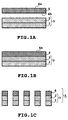
- Figures 1A through 1C are schematic cross-sectional views illustrating in the order the steps of the first method of manufacture of IC chips according to the present invention.
- Figures 2A through 2D are schematic cross-sectional views illustrating in the order the steps of the second method of manufacture of IC chips according to the present invention.
- the reinforcing material for silicon wafer according to the present invention and the method of manufacture of IC chips using said reinforcing material are explained below.
- the reinforcing material for silicon wafers according to the present invention is comprised of base material and adhesive for attaching said base material to silicon wafers. Damage prevention of silicon wafers during dicing can be realized by attaching the reinforcing material to the surface of a silicon wafer on which circuits are not formed (to be called the bottom surface of a silicon wafer hereafter), and dicing the silicon wafer and the reinforcing material simultaneously.
- the Rockwell hardness of the reinforcing material should be 60 or above in order to obtain sufficient reinforcing effect using the reinforcing material of the present invention.
- the term "Rockwell hardness (to be called HRM hereafter)" here in this specification is used as a unit for evaluation of hardness of reinforcing materials, determined according to the method described below.
- base material comprising the reinforcing material according to the present invention
- sheet-formed base materials of metal foils such as stainless steel or copper, fiber-reinforced plastics, liquid crystalline polymers, engineering plastics such as polyimide or polyethersulfone, plastics such as polypropylene or polyethylene
- Fibers such as glass fiber, metal fibers, and plastic fibers can also be used.
- thermosetting adhesives such as epoxy resins, phenol resins, urea resins and melamine resins
- curing agents added to these thermosetting adhesives for example, dicyandiamide, polyamide, and phthalic anhydride can be cited. These curing agents are preferably added in the ratio of 1 to 200 parts by weight for 100 parts by weight of thermosetting resins. Curing of thermosetting adhesives can be achieved by heat-treatment in the temperature range of 50 °C to 300 °C, more preferably 100 °C to 250 °C, for 10 seconds to 6 hours, though not particularly limited.
- Photo-curable adhesives based upon such polymers as (meth)acrylates and epoxy resins as the main polymer can also be used.
- the photo-polymerization initiators added to these photo-curable adhesives there are benzoin, acetophenone, and benzophenone, that are preferably added to the main polymer in the ratio of 0.001 to 10 parts by weight for 100 parts by weight of the main polymer.
- Curing of photo-curable adhesives can be achieved by photo-irradiation.
- the light source used for photo-irradiation for example, incandescent lamps, carbon arc lamps, fluorescent lamps, mercury lamps, xenon lamps, and fusion H lamps can be cited.
- Conditions of photo-irradiation are usually intensity of irradiation of 30 w/cm to 500 w/cm, distance of irradiation of 1 cm to 50 cm, and irradiation time of 0.1 second to 600 seconds, though not particularly limited.
- the first embodiment 1 is a reinforcing material comprised of a base material sheet with HRM of 60 or above, and an adhesive provided on one side of said base material sheet.
- the thickness of the base material sheet is, for example, 1 to 100 ⁇ m, more preferably 5 to 70 ⁇ m, though not particularly limited.
- the thickness of the adhesive provided on one side of the base material sheet is, for example, 1 to 50 ⁇ m, more preferably 5 to 35 ⁇ m, though not particularly limited.
- the method of providing adhesives on said base material sheet is not particularly limited, and can be carried out by well-known methods.
- the adhesive is applied directly on the base material sheet by potting, or uniformly applied using a knife-coater or a T-die extruder.
- heat-treatment is carried out in the temperature range of 30 °C to 150 °C for 30 seconds to 2 hours to remove the solvent after application of the adhesive.
- an adhesive can be applied on a process material having release property to form an adhesive sheet by the above-mentioned method, and then the adhesive sheet is then attached to the base material sheet.
- the sheet can be attached by pressurizing in a range of 10 Pa to 100 MPa using a press machine or a roll press machine in a temperature range of -40 °C to 150 °C.
- the second embodiment is a reinforcing material comprised of a base material sheet and a curable adhesive provided on one side of said base material sheet, of which HRM after the curable adhesive is cured is 60 or above.
- the thickness of the base material sheet is, for example, 1 to 100 ⁇ m, more preferably 5 to 70 ⁇ m, though not particularly limited.
- the thickness of the adhesive layer provided on one side of the base material sheet is, for example, 1 to 200 ⁇ m, more preferably 5 to 100 ⁇ m, though not particularly limited.
- base material sheets with HRM of less than 60 such as polyethylene (HRM 40) can be used.
- thermosetting adhesives or photo-curable adhesives described above can be used as said curable adhesive, thermosetting epoxy adhesives with excellent tensile strength, flexural strength, and impact strength after curing is preferably used.
- Manufacture of reinforcing materials in said second embodiment can be carried out in the same way as said first embodiment.
- the reinforcing material is comprised of a base material consisting of fibers impregnated with a curable adhesive, of which the HRM after the curable adhesive is cured is 60 or above.
- the reinforcing material can be either fibers formed into sheets and impregnated with curable adhesive, or cut fibers mixed with curable adhesive and formed into sheets.
- the thickness of the reinforcing material is 20 to 150 ⁇ m, more preferably 50 to 100 ⁇ m, though not particularly limited.
- the amount of the curable adhesive used for the amount of fibers is 10 to 500 parts by weight, preferably 20 to 200 parts by weight, of curable adhesive for 100 parts by weight of fibers, though not particularly limited.
- amount of curable adhesive used for 100 parts by weight of fibers is less than 10 parts by weight, required Rockwell strength cannot be obtained, and when it surpasses 500 parts by weight, the reinforcing material becomes brittle and easy to break.
- thermosetting adhesives or photo-curable adhesives described above can be used as the curable adhesive, thermosetting epoxy adhesives with excellent tensile strength, flexural strength, and impact strength after curing is preferably used.
- manufacture of the reinforcing material is carried out by the method of uniformly applying a mixture of fiber and curable adhesive on a process material with release property using a knife coater or a T-die extruder, or by the method of impregnating the fiber formed into sheets in advance with curable adhesive using a roll coater or a knife coater.
- Figures 1A through 1C are schematic cross-sectional views illustrating in the order the steps of the first method of manufacture of IC chips according to the present invention.
- the first method of manufacture includes:
- Figures 2A through 2D are schematic cross-sectional views illustrating in the order the steps of the second method of manufacture of IC chips according to the present invention.
- the second method of manufacture includes:
- the reinforcing material 6 is prepared either by impregnating fibers formed into sheets with curable adhesives or by extruding a mixture of fibers and curable adhesives in a form of sheet. Curing of curable adhesives can be achieved by heating when thermosetting adhesive is used and by photo-irradiation when photo-curable adhesive is used respectively.
- the arrows in Figure 2C schematically show heat-treatment or photo-irradiation for reinforcing material impregnated with curable adhesives.
- IC chips can be manufactured by providing a step of curing of the adhesive as in the second method of manufacture described above.
- IC chips since both the silicon wafer and the reinforcing material attached to the bottom side of said silicon wafer are diced together, not only prevention of damage of silicon wafers during dicing can be prevented but also IC chips provided with reinforcing materials can be obtained in an easier way than before. Moreover, the IC chips obtained are provided with the same size of reinforcing materials. Therefore, they can be handled in the same way as the conventional IC chips in the steps after dicing, and can be effectively prevented from damages.
- the Rockwell hardness tests were carried out according to the scale M of JIS K7202 "Rockwell hardness test of plastics".
- the reinforcing material comprised of the base material sheet and the adhesive provided on one side of said base material sheet is loaded from the base material sheet side.
- the reinforcing material (single layer structure in this case) comprised of base material comprising fibers and a curable adhesive is loaded from an optional side. Further, when curable adhesive was used, determination was carried out after curing of the adhesive.
- the Rockwell hardness vales determined by the above-mentioned method indicate higher hardness as the values are higher, with the upper limit of 200. Determined values of Rockwell hardness higher than 200 are indicated as 200 or more.
- test pieces of silicon wafer diced in a size of 5 mm by 5 mm were placed on a 2 mm thick of nitrile rubber sheet, 1.0 mm diameter of copper balls were placed on them and damage of the chips when loads of 3N were applied were examined.
- Example 1 illustrates a method of manufacture of an IC chip 5 by forming a reinforcing material 3 comprised of a base material sheet 1 and adhesive 2 provided on one side of said base material sheet 1, and then attaching it to a silicon wafer before dicing.
- thermoplastic polyimide resin adhesive 2 was applied to one side of a 30 ⁇ m stainless steel foil as the base material sheet 1 to form reinforcing material 3, that was die-cut to obtain a 5 inch diameter disc.
- a 50 ⁇ m thick of 5 inch diameter silicon wafer 4 was separately prepared.
- the adhesive 2 side of the cut reinforcing material 3 was attached to the bottom side 4b of the silicon wafer 4. Then the silicon wafer 4 and the reinforcing material 3 were completely attached by heating under a pressure of 5 kPa at 230 °C for 30 minutes.
- the silicon wafer 4 provided with reinforcing material 3 was diced to form 5 mm by 5 mm square IC chips 5 using a wafer-dicing machine A-WD4000B from Tokyo Seimitsu Co. Ltd.
- the IC chips obtained were inspected with a reflection microscope to find no cracks of 5 ⁇ m or above.
- Example 2 was carried out in the same way as Example 1 except that the reinforcing material 3 was prepared by applying polydimethylsiloxane-based pressure sensitive adhesive as adhesive 2 on one side of a 50 ⁇ m thick of polyimide film as the base material sheet 1 so that the thickness after drying is 20 ⁇ m.
- adhesion of the reinforcing material 3 and silicon wafer 4 was carried out by pressurizing at 5kPa using a press roller and then heating at 80 °C for 3 minutes.
- IC chips were obtained from the silicon wafer 4 provided with the reinforcing material 3 in the same way as Example 1, and observation showed no crack of 5 ⁇ m or more on the IC chips.
- Example 3 was carried out in the same way as Example 1 except that the reinforcing material 3 was prepared by attaching an 82 ⁇ m thick sheet-formed adhesive 2 made of thermosetting epoxy resin to one side of 20 ⁇ m thick polyethylene film as base material sheet 1.
- the thermosetting epoxy resin sheet as the adhesive 2 is prepared by adding 10 parts by weight of dicyandiamide as a curing agent to 100 parts by weight of bisphenol A-based epoxy resin, mixing and molding by extrusion.
- Adhesion of the reinforcing material 3 and the silicon wafer 4 was carried out at 120 °C for 60 minutes. During this, curing of the adhesive 2 occurred by heating.
- IC chips 5 were obtained from the silicon wafer 4 provided with the reinforcing material 3 in the same way as Example 1, and observation showed no crack of 5 ⁇ m or more on the IC chips.
- Example 4 illustrates a method of manufacture of IC chips 7 provided with reinforcing material 6 prepared by mixing fibers with thermosetting adhesive and forming into a sheet.
- thermosetting adhesive To 100 parts by weight of bisphenol-A-based epoxy resin, 60 parts by weight of polyamide was added as a curing agent to form a thermosetting adhesive, mixed with 100 parts by weight of glass fiber with fiber diameter of 10 ⁇ m and length of 20 mm to be the base material, and extrusion-molded to prepare 100 ⁇ m thick glass fiber sheet to be the reinforcing material 6 impregnated with thermosetting epoxy resin. Then the reinforcing material 6 obtained was die-cut into a 5 inch diameter disc. Also a 50 ⁇ m thick 5 inch diameter silicon wafer 4 was prepared.
- thermosetting adhesive Next, the bottom side 4b of silicone wafer 4 and the die-cutting reinforcing material 6 were attached. And then, the silicone wafer 4 and the die-cutting reinforcing material 6 were adhered by heating at 200 °C for 30 minutes thereby curing the thermosetting adhesive.
- IC chips 7 were obtained from the silicon wafer 4 provided with the reinforcing material 6 in the same way as Example 1, and observation showed no crack of 5 ⁇ m or more on the IC chips.
- Comparative example 1 was carried out in the same way as Example 1 except that the reinforcing material 3 was prepared using 80 ⁇ m thick polyethylene film as the base material sheet, and applying acrylic ester-base pressure sensitive adhesive as the adhesive 2 on one side of said polyethylene film to be the thickness of 20 ⁇ m after drying. Adhesion of reinforcing material 3 and silicon wafer 4 was carried out by pressurizing at 5kPa using a press roller and then heating at 80 °C for 3 minutes.
- IC chips 5 were obtained from the silicon wafer 4 provided with the reinforcing material 3 in the same way as Example 1, and observation showed cracks of 5 ⁇ m or more at the ends of five IC chips out of 100 IC chips.
- a silicon wafer having 50 ⁇ m of thick and 5 inch of diameter 4 was prepared and was diced to form 5 mm by 5 mm square IC chips 5 using a wafer-dicing machine A-WD4000B from Tokyo Seimitsu Co. Ltd.
- the IC chips obtained were inspected with a reflection microscope to find cracks of 5 ⁇ m or more at the ends of 32 IC chips out of 100 IC chips. Chip break test of IC chips 5 obtained was carried out. The results are shown in Table 1.
- HRM of reinforcing material Chip break test result Example 1 200 or more 0
- Example 4 95 0 Comparative example 1 40 65 Comparative example 2 - 99
- providing the bottom side of silicon wafer with reinforcing material prior to dicing of the silicon wafer enables to prevent damage of silicon wafer during dicing and greatly reduce chip break to occur, and enables to provide reinforcing material that enables improvement of productivity. It also enables to provide method of manufacture of IC chips that do not break during picking-up after dicing, during mounting on substrate circuits, and during wire bonding.
Landscapes
- Dicing (AREA)
- Adhesives Or Adhesive Processes (AREA)
- Credit Cards Or The Like (AREA)
Abstract
Description
| HRM of reinforcing material | Chip break test result | |
| Example 1 | 200 or more | 0 |
| Example 2 | 92 | 0 |
| Example 3 | 75 | 0 |
| Example 4 | 95 | 0 |
| Comparative example 1 | 40 | 65 |
| Comparative example 2 | - | 99 |
Claims (7)
- Reinforcing material for silicon wafer being attached, prior to dicing of said silicon wafer on which circuits are formed, to one side of said silicon wafer on which circuits are not formed,
wherein said reinforcing material is comprised of base material and adhesive, and has Rockwell hardness of 60 or above. - The reinforcing material according to Claim 1, wherein said adhesive is provided on one side of said base material.
- The reinforcing material according to Claim 1, wherein said adhesive is impregnated in said base material.
- The reinforcing material according to Claim 1, wherein said base material has Rockwell hardness of 60 or above.
- The reinforcing material according to Claim 1, wherein said adhesive is curable adhesive and Rockwell hardness of said reinforcing material after curing of said curable adhesive is 60 or above.
- Method of manufacture of IC chips comprising the steps of:wherein said reinforcing material is comprised of base material and adhesive, and has Rockwell hardness of 60 or above.providing reinforcing material on the side of said silicon wafer on which circuits are not formed, prior to dicing of silicon wafer on which circuits are formed; anddicing both said silicon wafer and reinforcing material provided on said silicon wafer,
- The method of manufacture of IC chips according to Claim 6 further comprising the steps of curing said adhesive of said reinforcing material prior to dicing of said silicon wafer.
Applications Claiming Priority (5)
| Application Number | Priority Date | Filing Date | Title |
|---|---|---|---|
| JP2000126609 | 2000-04-26 | ||
| JP2000126609 | 2000-04-26 | ||
| JP2001124757 | 2001-04-23 | ||
| JP2001124757A JP2002033296A (en) | 2000-04-26 | 2001-04-23 | Reinforcing member for silicon wafer, and method for manufacturing ic chip using the reinforcing member |
| PCT/JP2001/003557 WO2001082352A1 (en) | 2000-04-26 | 2001-04-25 | Reinforcement material for silicon wafer and method of manufacturing ic chip using the reinforcement material |
Publications (2)
| Publication Number | Publication Date |
|---|---|
| EP1193744A1 true EP1193744A1 (en) | 2002-04-03 |
| EP1193744A4 EP1193744A4 (en) | 2007-08-29 |
Family
ID=26590897
Family Applications (1)
| Application Number | Title | Priority Date | Filing Date |
|---|---|---|---|
| EP01925894A Withdrawn EP1193744A4 (en) | 2000-04-26 | 2001-04-25 | SILICON WAFER REINFORCING MATERIAL AND METHOD OF MANUFACTURING AN INTEGRATED MICROCIRCUIT USING THE MATERIAL |
Country Status (7)
| Country | Link |
|---|---|
| US (1) | US6765289B2 (en) |
| EP (1) | EP1193744A4 (en) |
| JP (1) | JP2002033296A (en) |
| KR (1) | KR100814536B1 (en) |
| CN (1) | CN1161823C (en) |
| TW (1) | TW490720B (en) |
| WO (1) | WO2001082352A1 (en) |
Families Citing this family (11)
| Publication number | Priority date | Publication date | Assignee | Title |
|---|---|---|---|---|
| US6503847B2 (en) * | 2001-04-26 | 2003-01-07 | Institute Of Microelectronics | Room temperature wafer-to-wafer bonding by polydimethylsiloxane |
| JP4153325B2 (en) * | 2003-02-13 | 2008-09-24 | 株式会社ディスコ | Semiconductor wafer processing method |
| ES2672648T3 (en) * | 2005-04-06 | 2018-06-15 | Hyet Energy Systems B.V. | Process for manufacturing parts of a sheet that has an inorganic coating of tco |
| KR100722547B1 (en) * | 2006-06-02 | 2007-06-27 | 한경대학교 산학협력단 | Internal reinforcement of surface modified FRP reinforcement and PC culvert using this FRP reinforcement |
| JPWO2010143614A1 (en) * | 2009-06-10 | 2012-11-22 | 旭硝子株式会社 | Manufacturing method of solar cell module |
| US9594999B2 (en) * | 2012-04-03 | 2017-03-14 | X-Card Holdings, Llc | Information carrying card comprising crosslinked polymer composition, and method of making the same |
| US9122968B2 (en) | 2012-04-03 | 2015-09-01 | X-Card Holdings, Llc | Information carrying card comprising a cross-linked polymer composition, and method of making the same |
| EP2973236B1 (en) | 2013-03-15 | 2019-01-09 | X-Card Holdings, LLC | Methods of making a core layer for an information carrying card, and resulting products |
| WO2019173455A1 (en) | 2018-03-07 | 2019-09-12 | X-Card Holdings, Llc | Metal card |
| US12220897B2 (en) | 2022-10-20 | 2025-02-11 | X-Card Holdings, Llc | Core layer for information carrying card, resulting information carrying card, and methods of making the same |
| US12528279B2 (en) | 2022-10-20 | 2026-01-20 | X-Card Holdings, Llc | Core layer for information carrying card, resulting information carrying card, and methods of making the same |
Family Cites Families (20)
| Publication number | Priority date | Publication date | Assignee | Title |
|---|---|---|---|---|
| EP0183016B1 (en) * | 1984-10-03 | 1989-09-20 | Sumitomo Electric Industries Limited | Material for a semiconductor device and process for its manufacture |
| JPH07105433B2 (en) * | 1986-05-20 | 1995-11-13 | 三井東圧化学株式会社 | Wafer processing film attachment method |
| JPH06209058A (en) * | 1993-01-12 | 1994-07-26 | Mitsubishi Electric Corp | Semiconductor device, manufacturing method thereof, and mounting method thereof |
| JPH06268112A (en) * | 1993-03-10 | 1994-09-22 | Mitsubishi Electric Corp | Semiconductor device and manufacturing method thereof |
| JPH09503622A (en) * | 1993-09-30 | 1997-04-08 | コピン・コーポレーシヨン | 3D processor using transfer thin film circuit |
| KR19990028523A (en) * | 1995-08-31 | 1999-04-15 | 야마모토 히데키 | Method for peeling protective adhesive tape of semiconductor wafer and its device |
| US5851845A (en) * | 1995-12-18 | 1998-12-22 | Micron Technology, Inc. | Process for packaging a semiconductor die using dicing and testing |
| US6784023B2 (en) * | 1996-05-20 | 2004-08-31 | Micron Technology, Inc. | Method of fabrication of stacked semiconductor devices |
| JP3928753B2 (en) * | 1996-08-06 | 2007-06-13 | 日立化成工業株式会社 | Multi-chip mounting method and manufacturing method of chip with adhesive |
| JP3755617B2 (en) * | 1996-08-30 | 2006-03-15 | 日立化成工業株式会社 | Wafer holding film for dicing |
| JPH10138671A (en) * | 1996-11-12 | 1998-05-26 | Citizen Watch Co Ltd | Module for ic card |
| JPH10321563A (en) * | 1997-05-16 | 1998-12-04 | Nitto Denko Corp | Semiconductor wafer holding sheet and semiconductor chip forming method |
| JPH1167699A (en) * | 1997-08-13 | 1999-03-09 | Texas Instr Japan Ltd | Method for manufacturing semiconductor device |
| JP2000017531A (en) * | 1998-06-23 | 2000-01-18 | Toyobo Co Ltd | Polyester combined filament yarn having excellent deep color dyeability and woven or knit fabric produced by using the filament yarn |
| JP3784202B2 (en) * | 1998-08-26 | 2006-06-07 | リンテック株式会社 | Double-sided adhesive sheet and method of using the same |
| JP2000077361A (en) * | 1998-08-27 | 2000-03-14 | Sharp Corp | Dicing method for semiconductor wafer |
| JP3441382B2 (en) * | 1998-10-14 | 2003-09-02 | 日本電信電話株式会社 | Method for manufacturing semiconductor device |
| JP2000148960A (en) | 1998-11-18 | 2000-05-30 | Hitachi Ltd | Semiconductor device |
| JP2000239622A (en) * | 1999-02-24 | 2000-09-05 | Sekisui Chem Co Ltd | Post-curing adhesive tape for fixing IC chip reinforcing plate |
| JP2007000992A (en) * | 2005-06-27 | 2007-01-11 | Matsushita Electric Works Ltd | Body of electric power tool, and electric power tool |
-
2001
- 2001-04-23 JP JP2001124757A patent/JP2002033296A/en not_active Withdrawn
- 2001-04-25 WO PCT/JP2001/003557 patent/WO2001082352A1/en not_active Ceased
- 2001-04-25 EP EP01925894A patent/EP1193744A4/en not_active Withdrawn
- 2001-04-25 CN CNB018010873A patent/CN1161823C/en not_active Expired - Fee Related
- 2001-04-25 KR KR1020017016620A patent/KR100814536B1/en not_active Expired - Fee Related
- 2001-04-25 US US09/840,864 patent/US6765289B2/en not_active Expired - Fee Related
- 2001-04-26 TW TW090110026A patent/TW490720B/en not_active IP Right Cessation
Also Published As
| Publication number | Publication date |
|---|---|
| US20020031863A1 (en) | 2002-03-14 |
| KR100814536B1 (en) | 2008-03-17 |
| EP1193744A4 (en) | 2007-08-29 |
| KR20020032441A (en) | 2002-05-03 |
| US6765289B2 (en) | 2004-07-20 |
| WO2001082352A1 (en) | 2001-11-01 |
| TW490720B (en) | 2002-06-11 |
| CN1161823C (en) | 2004-08-11 |
| JP2002033296A (en) | 2002-01-31 |
| CN1366708A (en) | 2002-08-28 |
Similar Documents
| Publication | Publication Date | Title |
|---|---|---|
| KR101176431B1 (en) | Method for producing semiconductor chip with adhesive film, adhesive film for semiconductor used in the method, and method for producing semiconductor device | |
| CN101714513B (en) | Method for producing the semiconductor device | |
| JP5449622B2 (en) | Adhesive film, dicing die bonding film, and semiconductor processing method using the same | |
| CN101821833B (en) | Adhesive film for semiconductor, method for manufacturing semiconductor chip, and semiconductor device | |
| JP6312498B2 (en) | Dicing film, dicing die-bonding film, and semiconductor device manufacturing method | |
| JP5556070B2 (en) | Manufacturing method of semiconductor device using adhesive sheet integrated with dicing tape | |
| WO2010024121A1 (en) | Process for production of dicing/die bondind film | |
| US20070126129A1 (en) | Die bonding adhesive tape | |
| JP4059497B2 (en) | Die bonding adhesive film, dicing die bonding adhesive film, and semiconductor device | |
| US6765289B2 (en) | Reinforcement material for silicon wafer and process for producing IC chip using said material | |
| CN111004588A (en) | Dicing die bonding film | |
| JP2014082498A (en) | Manufacturing method of dicing die-bonding film | |
| CN108728000B (en) | Dicing die bonding film | |
| JP2010074129A (en) | Method of manufacturing semiconductor device and semiconductor device manufactured by the same, and dicing-tape integral type adhesive sheet | |
| JP5656741B2 (en) | Manufacturing method of dicing die-bonding film | |
| TWI439530B (en) | Thermosetting wafer bonding film, dicing wafer bonding film, and method of manufacturing semiconductor device | |
| CN111009488A (en) | Dicing die bonding film | |
| CN112210305B (en) | Die bonding film and dicing die bonding film | |
| WO2022186285A1 (en) | Film adhesive, integrated dicing/die bonding film, semiconductor device, and method for producing semiconductor device |
Legal Events
| Date | Code | Title | Description |
|---|---|---|---|
| PUAI | Public reference made under article 153(3) epc to a published international application that has entered the european phase |
Free format text: ORIGINAL CODE: 0009012 |
|
| AK | Designated contracting states |
Kind code of ref document: A1 Designated state(s): AT BE CH CY DE DK ES FI FR GB GR IE IT LI LU MC NL PT SE TR |
|
| 17P | Request for examination filed |
Effective date: 20020311 |
|
| RBV | Designated contracting states (corrected) |
Designated state(s): DE FR GB IT |
|
| A4 | Supplementary search report drawn up and despatched |
Effective date: 20070801 |
|
| RIC1 | Information provided on ipc code assigned before grant |
Ipc: H01L 23/00 20060101AFI20070726BHEP Ipc: H01L 23/31 20060101ALI20070726BHEP Ipc: H01L 21/68 20060101ALI20070726BHEP Ipc: H01L 21/78 20060101ALI20070726BHEP |
|
| 17Q | First examination report despatched |
Effective date: 20080929 |
|
| STAA | Information on the status of an ep patent application or granted ep patent |
Free format text: STATUS: THE APPLICATION IS DEEMED TO BE WITHDRAWN |
|
| 18D | Application deemed to be withdrawn |
Effective date: 20090210 |