EP1191683A2 - High frequency power amplifier module and wireless communication apparatus - Google Patents
High frequency power amplifier module and wireless communication apparatus Download PDFInfo
- Publication number
- EP1191683A2 EP1191683A2 EP01306974A EP01306974A EP1191683A2 EP 1191683 A2 EP1191683 A2 EP 1191683A2 EP 01306974 A EP01306974 A EP 01306974A EP 01306974 A EP01306974 A EP 01306974A EP 1191683 A2 EP1191683 A2 EP 1191683A2
- Authority
- EP
- European Patent Office
- Prior art keywords
- amplifying
- high frequency
- power amplifier
- frequency power
- terminal
- Prior art date
- Legal status (The legal status is an assumption and is not a legal conclusion. Google has not performed a legal analysis and makes no representation as to the accuracy of the status listed.)
- Withdrawn
Links
- 238000004891 communication Methods 0.000 title claims description 76
- 230000009977 dual effect Effects 0.000 claims abstract description 29
- 239000004065 semiconductor Substances 0.000 claims description 85
- 238000000034 method Methods 0.000 claims description 21
- 238000005513 bias potential Methods 0.000 claims description 16
- 238000006243 chemical reaction Methods 0.000 claims description 9
- 230000001360 synchronised effect Effects 0.000 claims 1
- 238000010586 diagram Methods 0.000 description 21
- 230000003321 amplification Effects 0.000 description 11
- 238000003199 nucleic acid amplification method Methods 0.000 description 11
- 230000001413 cellular effect Effects 0.000 description 9
- 230000009467 reduction Effects 0.000 description 9
- 230000005540 biological transmission Effects 0.000 description 8
- 238000012545 processing Methods 0.000 description 8
- 241001125929 Trisopterus luscus Species 0.000 description 5
- 230000008901 benefit Effects 0.000 description 5
- 238000010295 mobile communication Methods 0.000 description 5
- 238000005516 engineering process Methods 0.000 description 4
- 238000004519 manufacturing process Methods 0.000 description 4
- HODRFAVLXIFVTR-RKDXNWHRSA-N tevenel Chemical compound NS(=O)(=O)C1=CC=C([C@@H](O)[C@@H](CO)NC(=O)C(Cl)Cl)C=C1 HODRFAVLXIFVTR-RKDXNWHRSA-N 0.000 description 4
- 101710170231 Antimicrobial peptide 2 Proteins 0.000 description 3
- 239000000758 substrate Substances 0.000 description 3
- 230000007704 transition Effects 0.000 description 3
- 230000000694 effects Effects 0.000 description 2
- 238000002955 isolation Methods 0.000 description 2
- 238000012552 review Methods 0.000 description 2
- 229920006395 saturated elastomer Polymers 0.000 description 2
- 238000005549 size reduction Methods 0.000 description 2
- XUIMIQQOPSSXEZ-UHFFFAOYSA-N Silicon Chemical compound [Si] XUIMIQQOPSSXEZ-UHFFFAOYSA-N 0.000 description 1
- 229910008310 Si—Ge Inorganic materials 0.000 description 1
- 230000009471 action Effects 0.000 description 1
- 239000003990 capacitor Substances 0.000 description 1
- 239000000969 carrier Substances 0.000 description 1
- 230000008859 change Effects 0.000 description 1
- 238000001914 filtration Methods 0.000 description 1
- 125000005842 heteroatom Chemical group 0.000 description 1
- 239000002184 metal Substances 0.000 description 1
- 229910044991 metal oxide Inorganic materials 0.000 description 1
- 150000004706 metal oxides Chemical class 0.000 description 1
- 230000002093 peripheral effect Effects 0.000 description 1
- 230000010363 phase shift Effects 0.000 description 1
- 230000003252 repetitive effect Effects 0.000 description 1
- 230000000452 restraining effect Effects 0.000 description 1
- 230000008054 signal transmission Effects 0.000 description 1
- 229910052710 silicon Inorganic materials 0.000 description 1
- 239000010703 silicon Substances 0.000 description 1
- 229910000679 solder Inorganic materials 0.000 description 1
- 239000000126 substance Substances 0.000 description 1
- 238000012546 transfer Methods 0.000 description 1
Images







Classifications
-
- H—ELECTRICITY
- H04—ELECTRIC COMMUNICATION TECHNIQUE
- H04B—TRANSMISSION
- H04B1/00—Details of transmission systems, not covered by a single one of groups H04B3/00 - H04B13/00; Details of transmission systems not characterised by the medium used for transmission
- H04B1/06—Receivers
- H04B1/16—Circuits
- H04B1/18—Input circuits, e.g. for coupling to an antenna or a transmission line
-
- H—ELECTRICITY
- H03—ELECTRONIC CIRCUITRY
- H03F—AMPLIFIERS
- H03F3/00—Amplifiers with only discharge tubes or only semiconductor devices as amplifying elements
- H03F3/45—Differential amplifiers
- H03F3/45071—Differential amplifiers with semiconductor devices only
- H03F3/45076—Differential amplifiers with semiconductor devices only characterised by the way of implementation of the active amplifying circuit in the differential amplifier
- H03F3/4508—Differential amplifiers with semiconductor devices only characterised by the way of implementation of the active amplifying circuit in the differential amplifier using bipolar transistors as the active amplifying circuit
- H03F3/45085—Long tailed pairs
- H03F3/45089—Non-folded cascode stages
-
- H—ELECTRICITY
- H03—ELECTRONIC CIRCUITRY
- H03F—AMPLIFIERS
- H03F1/00—Details of amplifiers with only discharge tubes, only semiconductor devices or only unspecified devices as amplifying elements
- H03F1/08—Modifications of amplifiers to reduce detrimental influences of internal impedances of amplifying elements
- H03F1/22—Modifications of amplifiers to reduce detrimental influences of internal impedances of amplifying elements by use of cascode coupling, i.e. earthed cathode or emitter stage followed by earthed grid or base stage respectively
-
- H—ELECTRICITY
- H03—ELECTRONIC CIRCUITRY
- H03F—AMPLIFIERS
- H03F1/00—Details of amplifiers with only discharge tubes, only semiconductor devices or only unspecified devices as amplifying elements
- H03F1/32—Modifications of amplifiers to reduce non-linear distortion
- H03F1/3211—Modifications of amplifiers to reduce non-linear distortion in differential amplifiers
-
- H—ELECTRICITY
- H03—ELECTRONIC CIRCUITRY
- H03F—AMPLIFIERS
- H03F3/00—Amplifiers with only discharge tubes or only semiconductor devices as amplifying elements
- H03F3/20—Power amplifiers, e.g. Class B amplifiers, Class C amplifiers
- H03F3/24—Power amplifiers, e.g. Class B amplifiers, Class C amplifiers of transmitter output stages
- H03F3/245—Power amplifiers, e.g. Class B amplifiers, Class C amplifiers of transmitter output stages with semiconductor devices only
-
- H—ELECTRICITY
- H03—ELECTRONIC CIRCUITRY
- H03F—AMPLIFIERS
- H03F2200/00—Indexing scheme relating to amplifiers
- H03F2200/294—Indexing scheme relating to amplifiers the amplifier being a low noise amplifier [LNA]
-
- H—ELECTRICITY
- H03—ELECTRONIC CIRCUITRY
- H03F—AMPLIFIERS
- H03F2200/00—Indexing scheme relating to amplifiers
- H03F2200/372—Noise reduction and elimination in amplifier
-
- H—ELECTRICITY
- H03—ELECTRONIC CIRCUITRY
- H03F—AMPLIFIERS
- H03F2203/00—Indexing scheme relating to amplifiers with only discharge tubes or only semiconductor devices as amplifying elements covered by H03F3/00
- H03F2203/45—Indexing scheme relating to differential amplifiers
- H03F2203/45392—Indexing scheme relating to differential amplifiers the AAC comprising resistors in the source circuit of the AAC before the common source coupling
-
- H—ELECTRICITY
- H03—ELECTRONIC CIRCUITRY
- H03F—AMPLIFIERS
- H03F2203/00—Indexing scheme relating to amplifiers with only discharge tubes or only semiconductor devices as amplifying elements covered by H03F3/00
- H03F2203/45—Indexing scheme relating to differential amplifiers
- H03F2203/45544—Indexing scheme relating to differential amplifiers the IC comprising one or more capacitors, e.g. coupling capacitors
-
- H—ELECTRICITY
- H03—ELECTRONIC CIRCUITRY
- H03F—AMPLIFIERS
- H03F2203/00—Indexing scheme relating to amplifiers with only discharge tubes or only semiconductor devices as amplifying elements covered by H03F3/00
- H03F2203/45—Indexing scheme relating to differential amplifiers
- H03F2203/45702—Indexing scheme relating to differential amplifiers the LC comprising two resistors
Definitions
- the present invention relates to a high frequency power amplifier module having a plurality of amplifying systems, for example, a high frequency power amplifier device (high frequency power amplifier module) capable of performing linear amplification and non-linear amplification (saturation amplification) and a wireless communication apparatus in which the high frequency power amplifier module is built therein, and particularly to a technology effective for application to a cellular portable phone of a multi-mode and multi-band communication scheme or system, which has a plurality of communication functions different from one another in communication mode and frequency band.
- a high frequency power amplifier device capable of performing linear amplification and non-linear amplification (saturation amplification)
- a wireless communication apparatus in which the high frequency power amplifier module is built therein
- a single cellular phone a so-called dual mode portable phone has recently been used wherein a digital system such as an analog type AMPS (Advanced Mobile Phone Service) covering the whole of North America, which has heretofore been used, TDMA (Time Division Multiple Access), CDMA (Code Division Multiple Access) or the like is built therein.
- AMPS Advanced Mobile Phone Service
- TDMA Time Division Multiple Access
- CDMA Code Division Multiple Access
- GSM Global System for Mobile Communication
- FDD Frequency Division Duplex
- EDGE Enhanced Data Rates for GSM Evolution
- the EDGE has been described in "Nikkei Electronics” published by Nikkei Business Publications, Inc., the November 15, 1999 (no.757), P131, and the July 3, 2000 (no.733), P126 to P139 of the same issue.
- the former reference has described a speeded-up mobile communication service in various parts of the world.
- the present reference describes that the mobile communication service transitions from the second generation of ⁇ 9.6kbits/second to the third generation of ⁇ 2Mbits/second. Further, the reference describes that in Europe, the mobile communication service transitions to an EDGE (third generation) through a GPRS (General Packet Radio Service: 2.5th generation) corresponding to a data communication service based on packet communications in which the existing GSM network is expanded, whereas in the USA, the mobile communication service transitions from an IS-136 system (TDMA) to the EDGE and from an IS-95 system (CDMA) to a cdma2000, an IS-2000 and an HDR (High Data Rate).
- TDMA IS-136 system
- CDMA IS-95 system
- HDR High Data Rate
- the latter reference describes a size reduction in a wireless circuit of a cellular phone. Further, the reference describes that a control technology wherein a plurality of channels can simultaneously be used in a high-speed data transmission or communication service, has been developed, and also describes that in a system EDGE dedicated for a GSM-based data communication service, a modulation scheme is changed from GMSK to eight-phase PSK to increase frequency availability, thereby implementing 384kbits/second. Furthermore, the same reference discloses a reference board for a GSM cellular phone using a chip set of a superheterodyne system and a direct conversion system.
- Another advantage of the EDGE system resides in that since the EDGE system can be introduced by appropriating the basic system of GSM and partly changing a radio modulation system or scheme, it can be operated without introducing infrastructure. This would be attractive for many communication common carriers.
- the modulation scheme to be changed serves as a system in which 3 ⁇ /8-rotating8PSK (Phase Shift Keying) modulation is used in the EDGE system with respect to GMSK (Gaussian Minimum Shift Keying) modulation of the GSM system.
- GMSK Gausian Minimum Shift Keying
- the EDGE system is a system in which the GSM system has been upbuilt, it is desirable that a single cellular phone is capable of making phone calls through the use of the GSM system and the EDGE system. It is therefore necessary to incorporate an amplifier for the GSM system and an amplifier for the EDGE system in the cellular phone.
- the present inventors have discussed a high frequency power amplifier module wherein one amplifier circuit copes with the GSM system and the EDGE system. As a result, the present inventors have found the following problems to be solved.
- An object of the present invention is to provide a high frequency power amplifier module and a wireless communication apparatus, which are capable of causing a saturation-operated system and a linearly-operated system to coexist with each other within the same circuit.
- Another object of the present invention is to provide a high frequency power amplifier module and a wireless communication apparatus, which allow a GSM system (saturation operation) and an EDGE system (linear operation) to coexist with each other within the same circuit.
- a further object of the present invention is to provide a high frequency power amplifier module and a wireless communication apparatus, which have plural modes/plural bands configurations.
- an APC signal is applied to each of the control terminals of the load-side semiconductor amplifying elements of the amplifying stages, a fixed predetermined signal is inputted to the input terminal, and potentials between the first terminals and third terminals of the respective amplifying stages are respectively controlled by APC signals, whereby the gain in the EDGE mode can be controlled or suppressed while an adjacent channel leakage power standard is being satisfied, and the gains in the communication modes (GSM mode and EDGE mode) different from each other can be rendered approximate, thereby enabling stable multi-mode communications.
- a description will be made of an example of a wireless communication apparatus (corresponding to a dualmode-dualband wireless communication apparatus) wherein a mode switching circuit is operated to perform switching to either a phase-modulation circuit configuration (circuit configuration for saturation amplification, e.g., circuit configuration for EDGE) or a phase and amplitude-modulation circuit configuration (circuit configuration for linear amplification, e.g., circuit configuration for EDGE), whereby communications are carried out.
- a phase-modulation circuit configuration circuit configuration for saturation amplification, e.g., circuit configuration for EDGE
- a phase and amplitude-modulation circuit configuration circuit configuration for linear amplification, e.g., circuit configuration for EDGE
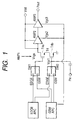
- FIG. 1 is a typical diagram showing a circuit configuration of a high frequency power amplifier module for performing mode switching.
- the high frequency power amplifier module according to the first embodiment corresponds to a high frequency power amplifier module having a dualband-dualmode configuration, which is capable of amplifying a GSM900 and a GSM1800, and an EDGE900 and an EDGE1800 selected according to mode switching.
- An amplification system takes a three-stage amplification configuration wherein amplifying stages (AMP1, AMP2 and AMP3) are successively cascade-connected.
- the amplifying stage (AMP1) corresponding to an initial or first stage is formed of semiconductor amplifying elements which comprise a load-side semiconductor amplifying element Tr1a and a ground-side semiconductor amplifying element Tr1b both connected in series.
- the Tr1 may be a dual-gate semiconductor amplifying element.
- MOS Metal Oxide Semiconductor
- silicon bipolar transistor a GaAs-MES (Metal-Semiconductor) FET
- HBT Hetero Junction Bipolar Transistor
- HEMT High Electron Mobility Transistor
- Si-Ge transistor etc.
- APC signals corresponding to two types (GSM900 and GSM1800) transmitted from a GSMPAC is sent to one contact of a selector switch SW1, and the other thereof is transmitted to one contact of a selector switch SW2. Further, the two types of APC signals sent from the GSMAPC control Vgs2 and Vgs3 of the AMP2 and AMP3.
- One of two types of EDGE signals (EDGE900 and EDGE1800) transmitted from an EDGEAPC is transmitted to the other contact of the selector switch SW1, and the other thereof is sent to the other contact of the selector switch SW2.
- An output terminal of the selector switch SW1 is connected to a control terminal (gate electrode) of Tr1a corresponding to the load-side semiconductor amplifying element of the AMP1 so that Vcgs is controlled. Further, an output terminal of the selector switch SW2 is connected to a control terminal (gate electrode) of Tr1b corresponding to the ground-side semiconductor amplifying element of the AMP1 so that Vgs1 is controlled.
- First terminals (drain electrodes) of the AMP1, AMP2 and AMP3 are respectively supplied with a first reference potential (Vdd).
- the control terminal (gate electrode) of the ground-side semiconductor amplifying element Tr1b of the AMP1 is supplied with an input signal.
- the output of the AMP3 is outputted to an output terminal Pout.
- the circuit having such a configuration serves as a high frequency power amplifier module capable of reducing or suppressing linear gain of EDGE in the case of the EDGE, thereby making the gain of the GSM and that of the EDGE substantially identical to each other, and allowing GSM-base communications and EDGE-based communications, both of which are low in distortion and noise and stable.
- the high frequency power amplifier module 20 has a rectangular structure flat in outer appearance.
- the high frequency power amplifier module 20 has a structure wherein a package 23 having a flat rectangular structure is formed or configured by a module substrate 21 made up of a plate-like wiring board, and a cap 22 attached to one surface (main surface) of the module substrate 21.
- the cap 22 is made of a metal which plays the role of an electromagnetic shield effect.
- Wiring patterns for the wiring board 21 and electronic components including semiconductor amplifying elements placed on the wiring board 21 constitute such a circuit as shown in FIG. 6.
- external electrode terminals are respectively provided over the peripheral surface of the high frequency power amplifier module 20 and the bottom face thereof.
- the external electrode terminals are of a surface-mount type and are formed of wirings formed on the module substrate 21 and solder formed on the surfaces thereof.
- Reference numeral 1 indicates a Vcgs-GSM 900 terminal
- reference numeral 2 indicates a non-contact terminal (N/C)
- reference numeral 3 indicates a Pout-GSM900 terminal
- reference numeral 4 indicates a Vdd-GSM900 terminal
- reference numeral 5 indicates a Vdd-GSM1800 terminal
- reference numeral 6 indicates a Pout-GSM1800 terminal
- reference numeral 7 indicates a mode switch or switching terminal (mode-SW)
- reference numeral 8 indicates a Vcgs-GSM1800 terminal
- reference numeral 9 indicates a Pin-GSM1800 terminal
- reference numeral 10 indicates a Vapc-GSM1800 terminal
- reference numeral 11 indicates a Vapc-GSM900 terminal
- reference numeral 12 indicates a Pin-GSM900 terminal
- G indicates a GND terminal, respectively.
- FIG. 6 is an equivalent circuit diagram of the high frequency power amplifier module (corresponding to transmit RF signal amplifying power amplifier) showing the first embodiment. As shown in the equivalent circuit diagram, it has an amplifying system a for the GSM900, and an amplifying system b for the GSM1800. In the amplifying systems a and b , switching is performed between circuit configurations according to a signal sent from the mode switch terminal (mode-SW). Thus, the GSM900 results in the EDGE900 and the GSM1800 results in the EDGE1800.
- mode-SW mode switch terminal
- the amplifying system a and the amplifying system b are different from each other in terms of the performance of the electronic components employed therein but are identical in circuit configuration. Accordingly, symbols applied to parts or components of the amplifying system b corresponding to the amplifying system a are shown inside the parentheses in the description of the amplifying system a , and this will be defined as the description of the amplifying system b .
- the external electrode terminals in the amplifying system a include a Pin-GSM900 (Pin-GSM1800 in the amplifying system b ) used as an input terminal, a Pout-GSM900 (Pout-GSM1800 in the amplifying system b ) used as an output terminal, a Vdd-GSM900 (Vdd-GSM1800 in the amplifying system b ), a Vcgs-GSM900 (Vcgs-GSM1800 in the amplifying system b ), a Vapc-GSM900 (Vapc-GSM1800 in the amplifying system b ), a mode switch terminal (mode-SW) used in common, and a GND terminal.
- a Pin-GSM900 Pin-GSM900
- Pout-GSM900 Pout-GSM1800 in the amplifying system b
- Vdd-GSM900 Vdd-GSM1800 in the amplifying system b
- Amplifying stages corresponding to three stages are cascade-connected between the Pin-GSM900 (Pin-GSM1800) and Pout-GSM900 (Pout-GSM1800).
- Each of the first stages comprises a dual gate MOSFET (Tr1: Tr10 in the amplifying system b ), and the second and third stages (output stages) respectively comprise single-gate MOSFETs (Tr2 and Tr3: Tr11 and Tr12 in the amplifying system b ).
- the first stages may respectively comprise load-side semiconductor amplifying elements and ground-side semiconductor amplifying elements connected in series, in place of the dual gate MOSFETs.
- load-side transistors and ground-side transistors of the dual gate MOSFETs will be explained without being marked with symbols in particular in the circuit configuration shown in FIG. 6.
- Control terminals of the load-side transistors will be called “first gate electrodes”
- control terminals of the ground-side transistors will be called "second gate electrodes”.
- the respective transistors which constitute the respective amplifying stages, respectively comprise first terminals (gate electrodes) for receiving input signals to the amplifying stages, and second terminals (drain electrodes) for transmitting output signals of the amplifying stages, and third terminals (source electrodes) for receiving a reference potential used for the amplifying stages.
- a plurality of temperature characteristic compensating circuits which respectively constitute current mirror circuits, are provided for the respective amplifying stages (Tr1, Tr2 and Tr3).
- the temperature characteristic compensating circuits respectively comprise transistors Tr4, Tr5 and Tr6 (Tr13, Tr14 and Tr15 in the amplifying system b ) whose gate and drain electrodes are connected to one another.
- a first gate electrode of the transistor Tr1 (Tr10 in the amplifying system b ) and a first gate electrode of a transistor Tr4 (Tr13 in the amplifying system b ) are connected to each other.
- the first gate electrode of the transistor Tr1 (Tr10 in the amplifying system b ) is connected to the Vcgs-GSM900 (Vcgs-GSM1800 in the amplifying system b ).
- a second gate electrode of the Tr1 (Tr10) is connected to the Pin-GSM900 (Pin-GSM1800 in the amplifying system b ) used as an input terminal.
- the second gate electrode of the Tr1 and the drain electrode of the load-side transistor of the Tr4 are connected to each other through a resistor R2.
- the Vapc-GSM900 (Vapc-GSM1800) and a second gate electrode of the Tr4 (Tr13) are connected to each other through a resistor R3 (resistor R16) and a resistor R4 (resistor R17) constituting a voltage dividing resistor.
- a wiring portion lying between the resistor R3 (resistor R16) and the resistor R4 (resistor R17) is connected to its corresponding drain electrode of the load-side transistor of the Tr4 (Tr13).
- the resistor R3 (resistor R16) and resistor R4 (resistor R17) constitute a bias circuit.
- the second gate electrode of the Tr4 (Tr13) and its corresponding drain electrode of a transistor Tr7 for the selector switch are connected to each other.
- a source electrode of the transistor Tr7 is grounded.
- a gate electrode of the transistor Tr7 is connected to a mode switch terminal (mode-SW) through a resistor R5 (resistor R18).
- the second stage is different from the first stage in terms of the dual mode MOSFET and the single gate MOSFET, the second stage is provided with a transistor Tr8 (Tr17) for the selector switch, whose gate electrode is connected to its corresponding mode switch terminal.
- a source electrode of the transistor Tr8 (Tr17) is grounded, and a drain electrode thereof is connected to its corresponding gate electrode of the Tr5 (Tr14) constituting a current mirror circuit.
- a drain electrode of the Tr5 (Tr14) is connected to its corresponding gate electrode of the Tr2 (Tr11).
- Vapc-GSM900 (Vapc-GSM1800) and the gate electrode of the Tr5 (Tr14) are connected to each other with a resistor R7 (R20) and a resistor R6 (resistor R19) constituting a voltage dividing resistor being interposed therebetween.
- a wiring portion lying between the resistor R7 (resistor R20) and the resistor R6 (resistor R19) is connected to its corresponding drain electrode of the Tr5 (Tr14).
- the resistor R7 (R20) and resistor R6 (resistor R19) constitute a bias circuit.
- the third stage is provided with a transistor Tr9 (Tr18) for the selector switch, whose gate electrode is connected to its corresponding mode switch terminal.
- a source electrode of the transistor Tr9 (Tr18) is grounded, and a drain electrode thereof is connected to its corresponding gate electrode of the Tr6 (Tr15) constituting a current mirror circuit.
- a drain electrode of the Tr6 (T15) is connected to its corresponding gate electrode of the Tr3 (Tr12) through a resistor R13 (R26).
- the Vapc-GSM900 (Vapc-GSM1800) and the gate electrode of the Tr6 (Tr15) are connected to each other with a resistor R10 (R23) and a resistor R11 (resistor R24) constituting a voltage dividing resistor being interposed therebetween.
- a wiring portion lying between the resistor R10 (resistor R23) and the resistor R11 (resistor R24) is connected to its corresponding drain electrode of the Tr6 (Tr15).
- the resistor R10 (R23) and resistor R11 (resistor R24) constitute a bias circuit.
- the load-side transistor of the Tr1 (Tr10) and the drain electrodes of the Tr2 (Tr11) and Tr3 (Tr12) are respectively connected to the Vdd-GSM900 (Vdd-GSM1800) so as to be supplied with a first reference potential (Vdd).
- the Tr7, Tr8 and Tr9 (Tr16, Tr17 and Tr18) constitute a mode switching circuit.
- L1 through L14 in the circuit diagram indicate impedance matching circuits respectively.
- FIG. 7 is a block diagram showing a part of the wireless communication apparatus and illustrates portions from a high-frequency signal processing IC (RF linear) 26 to an antenna (Antenna) 36.
- RF linear high-frequency signal processing IC
- Antenna antenna
- the antenna 36 is connected to an antenna terminal e of an antenna transmit-receive selector 40.
- the antenna terminal e and a transmit-receive selector switch 35 are electrically connected to each other.
- the transmit-receive selector switch 35 is operated according to a switch signal supplied to a control terminal ct1 to thereby change a switch to either an a terminal 35a or a b terminal 35b.
- a circuit system coupled to the a terminal 35a constitutes a transmission-system circuit
- a circuit system connected to the b terminal 35b constitutes a reception-system circuit. Namely, a capacitor C is interposed between a receiving terminal RX of the antenna transmit-receive selector 40 and the b terminal 35b.
- a filter 37 and a low noise amplifier (LNA) 38 are successively connected between the receiving terminal RX and the high frequency signal processing IC26.
- the aforementioned high frequency power amplifier module (PA) 20 is provided in the transmission-system circuit.
- a signal sent from a base band 27 of the high frequency signal processing IC 26 is inputted to the high frequency power amplifier module 20 through a voltage-controlled oscillator (VCO) 28, a mixer 29, and an automatic gain control circuit (AGC circuit) 30.
- VCO voltage-controlled oscillator
- AGC circuit automatic gain control circuit
- the output of the high frequency power amplifier module 20 is outputted to an input terminal d of the antenna transmit-receive selector 40.
- the antenna transmit-receive selector 40 is provided with a filter 34 for filtering a signal outputted from the high frequency power amplifier module 20.
- the signal transmitted through the filter 34 is sent to the a terminal 35a of the transmit-receive selector switch 35.
- the high frequency power amplifier module 20 is controlled by an automatic power controller (APC circuit) 32.
- the APC circuit 32 is controlled by a CPU 31 operated based on a signal sent out from the high frequency signal processing IC 26.
- a variation in the output of the high frequency power amplifier module 20 is detected by a coupler 33. The detected value is fed back to the APC circuit 32.
- the APC circuit 32 sends a control signal to each of the AGC circuit 30 and the high frequency power amplifier module 20.
- the APC circuit 32 transmits a Vapc/AM signal to the high frequency power amplifier module 20.
- the high frequency signal processing IC 26 sends a VTXon signal and a GSM/EDGE mode switching signal to the high frequency power amplifier module 20.
- An RF signal sent from the base band 27 is amplified and controlled by the APC circuit 32, followed by transmission to the antenna 36 according to the switching operation of the transmit-receive selector switch 35.
- a signal received by the antenna 36 is transmitted through the receiving terminal RX according to the switching operation of the transmit-receive selector switch 35, followed by transmission to the high frequency signal processing IC 26 through the filter 37 and the LNA 38.
- the dualband configurations of the GSM900 and GSM1800 are adopted and the respective bands are switched over to a GSM system and an EDGE system according to on/off operations of the mode switching transistors to thereby allow wireless communications (GSM900, GSM1800, EDGE900 and EDGE1800) corresponding to four forms.
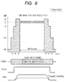
- FIG. 8 shows the time mask for the conventional GSM modulation system or scheme and illustrates the action of signals on the high frequency power amplifier module (power amp) incidental on it.
- power amp high frequency power amplifier module
- the power amp When the VTXon signal indicating of "Transmit it from the RF linear controller including the base band" is sent to the power amp, the power amp is brought to a standby state [corresponding to a state of being capable of varying output power (Pout) by the Vapc voltage] correspondingly.
- Pout of the power amp is power-controlled under Vapc voltage control according to the designation or instruction of a power class from a base station.
- GMSK modulation phase modulation
- phase information signal is carried out in a state in which power is constant in a certain class.
- the power amp is set to a standby state according to the VTXon signal (in this case, bias application capable of ensuring linearity is carried out) and AM modulation of EDGE is carried out under the Vapc voltage control in a manner similar to the power class control.
- the present mode is identical to the GSM mode in that the designation of the time mask by one slot is carried out and modulation is made with the power class as a given constant state.
- the GSM mode is identical in any of the operation examples but the EDGE mode is different therein as in the case of an EDGE mode 1, an EDGE mode 2, and an EDGE mode 3.
- the high frequency power amplifier module (power amp) 20 is used in a state shown in the block diagram of FIG. 7.
- Vcgs, Vgs1, Vgs2 and Vgs3, and Pin are respectively used in an APC state, an APC or fixed state, an APC state, and a fixed state in the GSM mode. Accordingly, it is not necessary to control the input signal sent to the power amp by AGC in the case of the GSM mode.
- the EDGE mode 1 is adopted as the EDGE mode.
- a desired potential is selected and fixed as Vcgs. Further, the Vgs1, Vgs2 and Vgs3 are fixed.
- the input signal Pin to be sent to the power amp is controlled by AGC.
- bias configurations of a circuit discussed in advance of the present invention are represented as shown in FIG. 17.
- Vcgs, Vgs1, Vgs2 and Vgs3 are used as APC, and Pin is used in a fixed state. Accordingly, AGC control becomes unnecessary.
- Vcgs, Vgs1, Vgs2 and Vgs3 are fixed, and Pin is AGC-controlled.
- Vgs1 is used as APC or fixed. However, it has the following features when Vgs1 is fixed.
- Vgs1 When Vgs1 is fixed, the impedance as viewed from the input (Pin) is stabilized.
- An advantage is brought about in that when the APC voltage is gradually reduced and Pout is reduced to about 1mW, the linearity of a first-stage FET can be maintained.
- a GSM900 mode needs to automatically power-control (APC) Vgs1, Vgs2 and Vgs3 of individual stages according to desired power classes.
- APC power-control
- mode-SW is set to a voltage (High) which ranges from about 2V to about 2.5V.
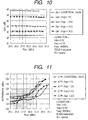
- FIG. 10 is a graph showing the correlation between EDGE output power and EDGEGain.
- Vdd 3.5V
- Vapc 2.2V
- the frequency 90MHz
- Pin control potential.
- the Gain of the EDGE can be varied according to potential control on Vcgs.
- FIG. 11 is a graph showing the correlation between EDGE output power and adjacent channel leakage power [ACPR: 400KHz (dBc)].
- the present operation example is an example in which the input power (Pin) is varied on condition that the bias is constant.
- a gain of 20dB or more can be reduced as compared with the initial state in which a Vcgs bias value is set identical upon the GSM operation.
- the bias circuit including the control gate of the first-stage dual gate MOSFET is used upon the use of the EDGE mode, and the bias circuits taking advantage of the current mirror circuits or the like are switched over according to the GSM and EDGE modes respectively, whereby the EDGE gain can be reduced prior to and subsequent to 35dB of a target under a three-stage configuration of the same chain as GSM. It is therefore possible to realize the amplification of the EDGE mode on a cellular phone actual device with gain of such an extent that no bad influence is exerted on noise or controllability.
- FIG. 12 a function configuration of a wireless communication apparatus is represented as shown in FIG. 12. Namely, while the input power to be sent to the power amp is controlled by the AGC circuit as shown in FIG. 7 in the operation example 1, input power is inputted directly to a power amp 20 from a mixer 29 in the operation example 2 as shown in FIG. 12.
- the EDGE mode results in the EDGE mode 2 as shown in FIG. 17.
- Vcgs is taken as APC, and Vgs1, Vgs2, Vgs3 and Pin are respectively used in a fixed state. Accordingly, the AGC control becomes unnecessary.
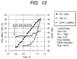
- FIG. 13 is a graph showing the correlation between output power and power amp efficiency (PAE) in the EDGE mode 2, and Vcgs of the first-stage dual gate. It is understood that as is apparent from this graph, power control can be realized in a state in which ACPR is held at -57dBc or less of a target. Namely, the AGC circuit which has heretofore been essential for the linear amp, becomes unnecessary. In a manner similar to upon the GSM operation, an APC voltage (Vcgs herein) can be power-controlled in a state in which the input power is constant.
- PEP power amp efficiency
- the input/output isolation of the amp at power OFF can be ensured by additionally turning ON/OFF Vapc at 0V and 2.2V in the form including the time mask of Vcgs through the use of the VTXon signal.
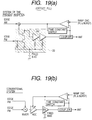
- FIG. 18 is a block diagram showing a present invention system in which the high frequency power amplifier module of the first embodiment is built and a conventional or prior art system in which an AGC circuit is built, under a direct conversion system or method.
- FIG. 19 is a block diagram showing a present invention system in which the high frequency power amplifier module of the first embodiment is built and a conventional or prior art system in which an AGC circuit is built, under an offset PLL system or method.
- control for keeping an antenna's output constant is realized by controlling the gain of an AGC amplifier placed in a stage preceding a power amplifier.
- control is implemented by controlling the control gate voltage of the first-stage dual gate FET lying within the power amplifier without having to use the AGC.
- EDGE-modulated AM/PM signal components outputted from a base band are combined together by a mixer. Thereafter, the combined signal is gain-controlled by an AGC amplifier, followed by input to a power amplifier. Control on an antenna's output is carried out by varying the gain of the AGC amplifier placed in a stage preceding the power amplifier.
- the signal processing and gain control are realized by controlling the control gate voltage of the first-stage dual gate FET lying within the power amplifier.
- the need for the mixer can also be eliminated as well as the AGC.
- both the offset PLL method and the direct conversion method eliminate the need for the AGC circuit.
- the mixer becomes also unnecessary. Namely, since the linearity based on the AM-amplitude using each Vcgs voltage can be ensured by use of the control gate as described up to now, the present embodiment has the mixer function of combining the PM-modulation from the input and the AM-modulation from Vcgs by means of the first-stage dual gate MOSFET.
- the AGC circuit or the AGC circuit and the mixer become unnecessary, the number of components of sets placed outside the power amplifier can greatly be reduced, and a reduction in the cost of the wiring communication apparatus can be achieved.
- FIG. 14 a function configuration of a wiring communication apparatus is represented as shown in FIG. 14. Namely, this indicates the state in which the VTXon signal transmitted from the high frequency signal processing IC 26 to the power amp 20 is omitted from the operation example 2.
- the EDGE mode is taken as the EDGE mode 3 as shown in FIG. 17.
- Vcgs, Vgs1, Vgs2 and Vgs3 are used as APC and Pin is used in a fixed state in the EDGE mode 3. Even in this case, the AGC control becomes unnecessary.
- FIG. 15 is a graph showing the correlation between Vapc employed in the operation example 3 and Vcgs of the first-stage dual gate.
- FIG. 16 is a graph showing the correlation between output power and ACPR with respect to Vapc employed in the operation example 3.
- an EDGE operation at the time that all gate biases are variable could be confirmed by holding the correlation of the graph in FIG. 15 while linearity of each amplifying stage is being maintained.
- an ACPR spec is defined as -57dBc or less.
- the present embodiment is not limited to or by the aforementioned operation examples.
- the transistor corresponding to the second stage of each amplifying system makes use of the dual gate MOSFET, and only Vcgs and Vgs3 corresponding to the third stage may be used for EDGEAPC control.
- FIG. 20 is a block diagram showing a circuit configuration of a high frequency amplifier module showing another embodiment (second embodiment) of the present invention.
- the present embodiment shows a one-input and two-output configuration wherein only a first-stage dual gate MOSFET is used in common and amplifying transistors corresponding to a second stage and subsequent to it are separated.
- the present example illustrates an example applied to GSM and W (Wideband)-CDMA.
- the sharing of the initial-stage transistor allows achievement of a less size reduction.
- the first stage may take a two-input and two-output configuration in parts. In this case, it is needless to say that since W-CDMA is linearly operated, the dual gate MOSFET is used as a matter of course.
Landscapes
- Engineering & Computer Science (AREA)
- Power Engineering (AREA)
- Physics & Mathematics (AREA)
- Nonlinear Science (AREA)
- Computer Networks & Wireless Communication (AREA)
- Signal Processing (AREA)
- Amplifiers (AREA)
- Control Of Amplification And Gain Control (AREA)
- Transceivers (AREA)
Abstract
Description
Claims (37)
- A high frequency power amplifier module comprising:an input terminal supplied with a signal to be amplified;an output terminal;a control terminal;a mode switch terminal;a plurality of amplifying stages cascade-connected between said input terminal and said output terminal,said plurality of amplifying stages respectively comprising first terminals each of which receives a signal inputted to said each amplifying stage, second terminals each of which transmits a signal outputted therefrom, and third terminals each of which receives a reference potential for said each amplifying stage;bias circuits which are respectively connected between said control terminal and the first terminals of said respective amplifying stages and respectively apply to the first terminals a dc bias potential based on a voltage supplied to said control terminal;a plurality of temperature characteristic compensating circuits which respectively constitute current mirror circuits with respect to said respective amplifying stages; anda mode switching circuit which is operated by a signal supplied to said mode switching terminal and turns on and off said each temperature characteristic compensating circuit to thereby perform switching between communication modes,wherein said one or more amplifying stages excluding the amplifying stage corresponding to a final stage, of said plurality of amplifying stages, and said temperature characteristic compensating circuits corresponding to said one or more amplifying stages respectively comprise load-side semiconductor amplifying elements and ground-side semiconductor amplifying elements connected in series, control terminals of the load-side semiconductor amplifying elements of said amplifying stages and control terminals of the load-side semiconductor amplifying elements of said temperature characteristic compensating circuits corresponding to said amplifying stages are respectively connected to one another, and each of control terminals of said ground-side semiconductor amplifying elements of said amplifying stages is connected between resistors forming a voltage dividing resistor of each of said bias circuits for said amplifying stages,an APC signal is applied to the control terminal of said load-side semiconductor amplifying element of said each amplifying stage in one communication mode so that the communication modes different from each other approximate each other in gain, andpredetermined fixed potentials are respectively applied to the first terminals of said respective amplifying stages as bias potentials.
- The high frequency power amplifier module according to claim 1, which is switched to either a phase-modulation circuit configuration or a phase and amplitude-modulation circuit configuration according to the operation of said mode switching circuit.
- The high frequency power amplifier module according to claim 1, which is switched to either a circuit configuration for a saturation amplifier or a circuit configuration for a linear amplifier according to the operation of said mode switching circuit.
- The high frequency power amplifier module according to claim 1, which is switched to either a circuit configuration for GSM or a circuit configuration for EDGE according to the operation of said mode switching circuit.
- The high frequency power amplifier module according to claim 1, wherein said plurality of amplifying stages, and said bias circuits and said temperature characteristic compensating circuits incidental thereon are provided in plural sets to thereby constitute a plurality of amplifying systems, and said respective amplifying stages of said plurality of amplifying systems are connected to said mode switching terminal to constitute a multi-mode and multi-band high frequency power amplifier device.
- The high frequency power amplifier module according to claim 1, wherein the amplifying stages each corresponding to a first stage, of said plurality of amplifying systems are provided in a shared configuration.
- The high frequency power amplifier module according to claim 1, wherein said load-side semiconductor amplifying element and said ground-side semiconductor amplifying element connected in series are dual gate type semiconductor amplifying elements.
- A high frequency power amplifier module comprising:an input terminal supplied with a signal to be amplified;an output terminal;a control terminal;a mode switch terminal;a plurality of amplifying stages cascade-connected between said input terminal and said output terminal,said plurality of amplifying stages respectively comprising first terminals each of which receives a signal inputted to said each amplifying stage, second terminals each of which transmits a signal outputted therefrom, and third terminals each of which receives a reference potential for said each amplifying stage;bias circuits which are respectively connected between said control terminal and the first terminals of said respective amplifying stages and respectively apply to the first terminals a dc bias potential based on a voltage supplied to said control terminal;a plurality of temperature characteristic compensating circuits which respectively constitute current mirror circuits with respect to said respective amplifying stages; anda mode switching circuit which is operated by a signal supplied to said mode switching terminal and turns on and off said each temperature characteristic compensating circuit to thereby perform switching between communication modes,wherein said one or more amplifying stages excluding the amplifying stage corresponding to a final stage, of said plurality of amplifying stages, and said temperature characteristic compensating circuits corresponding to said one or more amplifying stages respectively comprise load-side semiconductor amplifying elements and ground-side semiconductor amplifying elements connected in series, control terminals of the load-side semiconductor amplifying elements of said amplifying stages and control terminals of the load-side semiconductor amplifying elements of said temperature characteristic compensating circuits corresponding to said amplifying stages are respectively connected to one another, and each of control terminals of said ground-side semiconductor amplifying elements of said amplifying stages is connected between resistors forming a voltage dividing resistor of each of said bias circuits for said amplifying stages,an APC signal is applied to the control terminal of said load-side semiconductor amplifying element of said each amplifying stage in one communication mode so that the communication modes different from each other approximate each other in gain, andAPC signals are respectively applied to the first terminals of said respective amplifying stages as bias potentials.
- The high frequency power amplifier module according to claim 8, which is switched to either a phase-modulation circuit configuration or a phase and amplitude-modulation circuit configuration according to the operation of said mode switching circuit.
- The high frequency power amplifier module according to claim 8, which is switched to either a circuit configuration for a saturation amplifier or a circuit configuration for a linear amplifier according to the operation of said mode switching circuit.
- The high frequency power amplifier module according to claim 8, which is switched to either a circuit configuration for GSM or a circuit configuration for EDGE according to the operation of said mode switching circuit.
- The high frequency power amplifier module according to claim 8, wherein said plurality of amplifying stages, and said bias circuits and said temperature characteristic compensating circuits incidental thereon are provided in plural sets to thereby constitute a plurality of amplifying systems, and said respective amplifying stages of said plurality of amplifying systems are connected to said mode switching terminal to constitute a multi-mode and multi-band high frequency power amplifier device.
- The high frequency power amplifier module according to claim 8, wherein the amplifying stages each corresponding to a first stage, of said plurality of amplifying systems are provided in a shared configuration.
- The high frequency power amplifier module according to claim 8, wherein said load-side semiconductor amplifying element and said ground-side semiconductor amplifying element connected in series are dual gate type semiconductor amplifying elements.
- A high frequency power amplifier module comprising:an input terminal supplied with a signal to be amplified;an output terminal;a control terminal;a mode switch terminal;a plurality of amplifying stages cascade-connected between said input terminal and said output terminal,said plurality of amplifying stages respectively comprising first terminals each of which receives a signal inputted to said each amplifying stage, second terminals each of which transmits a signal outputted therefrom, and third terminals each of which receives a reference potential for said each amplifying stage;bias circuits which are respectively connected between said control terminal and the first terminals of said respective amplifying stages and respectively apply to the first terminals a dc bias potential based on a voltage supplied to said control terminal;a plurality of temperature characteristic compensating circuits which respectively constitute current mirror circuits with respect to said respective amplifying stages; anda mode switching circuit which is operated by a signal supplied to said mode switching terminal and turns on and off said each temperature characteristic compensating circuit to thereby perform switching between communication modes,wherein said one or more amplifying stages excluding the amplifying stage corresponding to a final stage, of said plurality of amplifying stages, and said temperature characteristic compensating circuits corresponding to said one or more amplifying stages respectively comprise load-side semiconductor amplifying elements and ground-side semiconductor amplifying elements connected in series, control terminals of the load-side semiconductor amplifying elements of said amplifying stages and control terminals of the load-side semiconductor amplifying elements of said temperature characteristic compensating circuits corresponding to said amplifying stages are respectively connected to one another, and each of control terminals of said ground-side semiconductor amplifying elements of said amplifying stages is connected between resistors forming a voltage dividing resistor of each of said bias circuits for said amplifying stages,a selected and fixed potential is applied to the control terminal of said load-side semiconductor amplifying element of said each amplifying stage in one communication mode so that the communication modes different from each other approximate each other in gain, andpredetermined fixed potentials are respectively applied to the first terminals of said respective amplifying stages as bias potentials.
- The high frequency power amplifier module according to claim 15, which is switched to either a phase-modulation circuit configuration or a phase and amplitude-modulation circuit configuration according to the operation of said mode switching circuit.
- The high frequency power amplifier module according to claim 15, which is switched to either a circuit configuration for a saturation amplifier or a circuit configuration for a linear amplifier according to the operation of said mode switching circuit.
- The high frequency power amplifier module according to claim 15, which is switched to either a circuit configuration for GSM or a circuit configuration for EDGE according to the operation of said mode switching circuit.
- The high frequency power amplifier module according to claim 15, wherein said plurality of amplifying stages, and said bias circuits and said temperature characteristic compensating circuits incidental thereon are provided in plural sets to thereby constitute a plurality of amplifying systems, and said respective amplifying stages of said plurality of amplifying systems are connected to said mode switching terminal to constitute a multi-mode and multi-band high frequency power amplifier device.
- The high frequency power amplifier module according to claim 15, wherein the amplifying stages each corresponding to a first stage, of said plurality of amplifying systems are provided in a shared configuration.
- The high frequency power amplifier module according to claim 15, wherein said load-side semiconductor amplifying element and said ground-side semiconductor amplifying element connected in series are dual gate type semiconductor amplifying elements.
- A wireless communication apparatus having a high frequency power amplifier module according to claim 1.
- The wireless communication apparatus according to claim 22, wherein said high frequency power amplifier module is used in a direct conversion method wherein a quadrature component signal and a synchronous component signal are inputted to an input terminal.
- The wiring communication apparatus according to claim 22, wherein said high frequency power amplifier module is used in an offset PLL method wherein an amplitude-modulated signal is directly inputted to a first gate of a dual gate transistor of a first-stage amplifying stage and a phase signal is directly inputted to a second gate thereof.
- A wireless communication apparatus having a high frequency power amplifier module according to claim 8.
- A wireless communication apparatus having a high frequency power amplifier module according to claim 15.
- A high frequency power amplifier module for performing a linear amplifying operation or a non-linear amplifying operation according to a communication mode signal, comprising:an input terminal supplied with a signal to be amplified;an output terminal;a mode switch terminal;a plurality of amplifying stages cascade-connected between said input terminal and said output terminal and having first terminals for respectively receiving input signals supplied to said amplifying stages, and second terminals for respectively sending out signals outputted from said amplifying stages;bias circuits which are respectively connected to the first terminals of said respective amplifying stages and apply bias potentials to the first terminals; anda mode switching circuit which forms a mode signal according to a communication mode signal supplied to said mode switch terminal;wherein at least one amplifying stage of said plurality of amplifying stages includes first and second semiconductor amplifying elements series-connected to one another, the first terminal of said amplifying stage is connected to a control input node of the second semiconductor amplifying element, and the second terminal thereof is connected to an output node of the first semiconductor amplifying element,the mode signal is supplied to the control input node of the first semiconductor amplifying element, andwhen the linear amplifying operation and the non-linear amplifying operation are performed, gain is controlled by the mode signal.
- The high frequency power amplifier module according to claim 27, which is operated as a saturation amplifier or a non-saturation amplifier according to the mode signal.
- The high frequency power amplifier module according to claim 27, which is operated as a GSM amplifier or an EDGE amplifier according to the mode signal.
- The high frequency power amplifier module according to claim 27, wherein the first and second semiconductor amplifying elements series-connected to each other are of a single dual gate type semiconductor amplifying element.
- A high frequency power amplifier module comprising:an input terminal supplied with a signal to be amplified;an output terminal;a mode terminal;a plurality of amplifying stages cascade-connected between said input terminal and said output terminal and having first terminals for respectively receiving input signals supplied to said amplifying stages, and second terminals for respectively sending out signals outputted from said amplifying stages;bias circuits which supply bias potentials to said respective amplifying stages respectively; anda mode circuit which forms an AGC signal according to a signal supplied to said mode terminal;wherein at least one of said amplifying stages has first and second semiconductor amplifying elements series-connected to one another, anda control terminal of the first semiconductor amplifying element is supplied with the AGC signal, an output terminal of the first semiconductor amplifying element is connected to the corresponding second terminal, and a control terminal of the second semiconductor amplifying element is connected to the corresponding first terminal.
- The high frequency power amplifier module according to claim 31, wherein the first and second semiconductor amplifying elements series-connected to one another are a single dual gate type semiconductor amplifying element.
- A high frequency power amplifier module comprising:an input terminal supplied with a signal to be amplified;an output terminal;a mode terminal;a plurality of amplifying stages cascade-connected between said input terminal and said output terminal and having first terminals for respectively receiving input signals supplied to said amplifying stages, and second terminals for respectively sending out signals outputted from said amplifying stages;bias circuits which supply bias potentials to said respective amplifying stages respectively; anda mode circuit which forms an APC signal according to a signal supplied to said mode terminal;wherein at least one of said amplifying stages has first and second semiconductor amplifying elements series-connected to one another, anda control terminal of the first semiconductor amplifying element is supplied with the APC signal, a control terminal of the second semiconductor amplifying element is connected to the corresponding first terminal and an output terminal of the first semiconductor amplifying element is connected to the corresponding second terminal.
- The high frequency power amplifier module according to claim 33, wherein the first and second semiconductor amplifying elements connected in series are a single dual gate type semiconductor amplifying element.
- A wireless communication apparatus having a high frequency power amplifier module according to claim 27.
- A wireless communication apparatus having a high frequency power amplifier module according to claim 31.
- A wireless communication apparatus having a high frequency power amplifier module according to claim 33.
Applications Claiming Priority (2)
| Application Number | Priority Date | Filing Date | Title |
|---|---|---|---|
| JP2000275605 | 2000-09-11 | ||
| JP2000275605A JP3895532B2 (en) | 2000-09-11 | 2000-09-11 | High frequency power amplifier and wireless communication device |
Publications (2)
| Publication Number | Publication Date |
|---|---|
| EP1191683A2 true EP1191683A2 (en) | 2002-03-27 |
| EP1191683A3 EP1191683A3 (en) | 2004-05-06 |
Family
ID=18761205
Family Applications (1)
| Application Number | Title | Priority Date | Filing Date |
|---|---|---|---|
| EP01306974A Withdrawn EP1191683A3 (en) | 2000-09-11 | 2001-08-16 | High frequency power amplifier module and wireless communication apparatus |
Country Status (5)
| Country | Link |
|---|---|
| US (1) | US6636114B2 (en) |
| EP (1) | EP1191683A3 (en) |
| JP (1) | JP3895532B2 (en) |
| KR (1) | KR20020020836A (en) |
| TW (1) | TW595234B (en) |
Cited By (4)
| Publication number | Priority date | Publication date | Assignee | Title |
|---|---|---|---|---|
| WO2003094343A1 (en) | 2002-04-30 | 2003-11-13 | Skyworks Solutions, Inc. | Dual mode power amplifier having a common controller |
| EP1693958A1 (en) * | 2005-02-16 | 2006-08-23 | EADS Deutschland GmbH | Method for operating a high-frequency amplifier |
| CN103477558A (en) * | 2011-08-31 | 2013-12-25 | 株式会社村田制作所 | Semiconductor integrated circuit device and high frequency power amplifier module |
| CN106533374A (en) * | 2016-09-20 | 2017-03-22 | 锐迪科微电子(上海)有限公司 | Multiband GSM radio-frequency power amplifier |
Families Citing this family (38)
| Publication number | Priority date | Publication date | Assignee | Title |
|---|---|---|---|---|
| US5754961A (en) | 1994-06-20 | 1998-05-19 | Kabushiki Kaisha Toshiba | Radio communication system including SDL having transmission rate of relatively high speed |
| JP2002111415A (en) * | 2000-09-29 | 2002-04-12 | Hitachi Ltd | High frequency power amplifier and wireless communication device |
| JP2003037454A (en) * | 2001-07-23 | 2003-02-07 | Hitachi Ltd | High frequency power amplifier circuit |
| US6914481B2 (en) * | 2001-11-26 | 2005-07-05 | Matsushita Electric Industrial Co., Ltd. | High frequency power amplifier apparatus and power amplifier module use the same |
| WO2003073627A1 (en) * | 2002-02-28 | 2003-09-04 | Renesas Technology Corp. | High-frequency power amplifier circuit and electronic part for communication |
| JP2003298360A (en) * | 2002-03-29 | 2003-10-17 | Hitachi Ltd | High frequency amplifier |
| GB0212740D0 (en) * | 2002-05-31 | 2002-07-10 | Hitachi Ltd | Transmitter and wireless communication apparatus using the transmitter |
| KR100704568B1 (en) * | 2002-08-05 | 2007-04-06 | 인티그런트 테크놀로지즈(주) | Variable gain low noise amplifier |
| EP1579569A1 (en) * | 2002-12-19 | 2005-09-28 | Koninklijke Philips Electronics N.V. | Power amplifier with bias control |
| JP2004343164A (en) | 2003-05-13 | 2004-12-02 | Renesas Technology Corp | Semiconductor integrated circuit for communication and radio communication system |
| JP4287193B2 (en) | 2003-05-15 | 2009-07-01 | 株式会社ルネサステクノロジ | Electronic component for high frequency power amplification and wireless communication system |
| DE60319511T2 (en) * | 2003-06-10 | 2009-03-26 | Sony Ericsson Mobile Communications Ab | Reduction of radiofrequency crosstalk |
| JP3841416B2 (en) * | 2003-10-07 | 2006-11-01 | 松下電器産業株式会社 | Transmission device, transmission output control method, and wireless communication device |
| US6888410B1 (en) * | 2003-10-10 | 2005-05-03 | Broadcom Corp. | Power amplifier having low gate oxide stress |
| US7304539B2 (en) * | 2003-10-16 | 2007-12-04 | Renesas Technology Corporation | High frequency power amplifier circuit and electronic component for high frequency power amplifier |
| US7177370B2 (en) | 2003-12-17 | 2007-02-13 | Triquint Semiconductor, Inc. | Method and architecture for dual-mode linear and saturated power amplifier operation |
| JP4394498B2 (en) | 2004-03-31 | 2010-01-06 | 株式会社ルネサステクノロジ | High frequency circuit device and mobile communication terminal using the same |
| JP4659826B2 (en) | 2004-06-23 | 2011-03-30 | ペレグリン セミコンダクター コーポレーション | RF front-end integrated circuit |
| WO2006038189A1 (en) * | 2004-10-08 | 2006-04-13 | Koninklijke Philips Electronics N.V. | Dual bias control circuit |
| US7164319B2 (en) * | 2005-04-29 | 2007-01-16 | Triquint Semiconductor, Inc. | Power amplifier with multi mode gain circuit |
| JP4750463B2 (en) * | 2005-05-11 | 2011-08-17 | ルネサスエレクトロニクス株式会社 | High frequency power amplifier, transmitter using the same, and mobile communication terminal |
| KR100756041B1 (en) * | 2005-06-27 | 2007-09-07 | 삼성전자주식회사 | Doherty Amplifier and Transmitter Using a Mixer |
| KR100751554B1 (en) | 2006-06-28 | 2007-08-23 | 엘지전자 주식회사 | Power amplification device and power amplification method of mobile communication terminal capable of dual band frequency input |
| US7446605B2 (en) * | 2006-09-27 | 2008-11-04 | Infineon Technologies Ag | Amplifier arrangement with controllable gain and method for controlling an amplifier gain |
| WO2008078468A1 (en) * | 2006-12-26 | 2008-07-03 | Panasonic Corporation | Transmitting device and communication device |
| KR100974574B1 (en) * | 2008-01-16 | 2010-08-06 | 한국과학기술원 | Resistive frequency mixing device and signal processing method using same |
| US8718582B2 (en) * | 2008-02-08 | 2014-05-06 | Qualcomm Incorporated | Multi-mode power amplifiers |
| JP5158425B2 (en) * | 2008-03-12 | 2013-03-06 | 株式会社村田製作所 | RF power amplifier |
| JP5131540B2 (en) * | 2008-05-20 | 2013-01-30 | 株式会社村田製作所 | RF power amplifier and RF power amplifier |
| CN201528316U (en) * | 2009-08-31 | 2010-07-14 | 华为终端有限公司 | Power amplifier as well as receiving device of user equipment |
| US8912847B2 (en) * | 2009-12-03 | 2014-12-16 | Epcos Ag | Power amplifier circuit and front end circuit |
| US8487706B2 (en) * | 2010-01-25 | 2013-07-16 | Peregrine Semiconductor Corporation | Stacked linear power amplifier with capacitor feedback and resistor isolation |
| US8350624B2 (en) | 2010-09-01 | 2013-01-08 | Peregrine Semiconductor Corporation | Amplifiers and related biasing methods and devices |
| US8368462B2 (en) | 2010-10-06 | 2013-02-05 | Peregrine Semiconductor Corporation | Method, system, and apparatus for RF switching amplifier |
| US9960737B1 (en) | 2017-03-06 | 2018-05-01 | Psemi Corporation | Stacked PA power control |
| CN209375663U (en) | 2018-12-19 | 2019-09-10 | 南京米乐为微电子科技有限公司 | A kind of wideband logarithmic detector of high dynamic range |
| CN111245371B (en) | 2020-03-06 | 2023-07-04 | 重庆百瑞互联电子技术有限公司 | Power mixer, radio frequency circuit, device and equipment |
| JP7068540B1 (en) * | 2021-12-16 | 2022-05-16 | 株式会社京三製作所 | High-frequency power supply and high-frequency power output control method |
Family Cites Families (9)
| Publication number | Priority date | Publication date | Assignee | Title |
|---|---|---|---|---|
| US5337019A (en) * | 1992-02-20 | 1994-08-09 | Siemens Aktiengesellschaft | Integrated circuit arrangement |
| GB2269716A (en) * | 1992-08-03 | 1994-02-16 | Texas Instruments Ltd | Bias circuit for changing class of part of multistage amplifier |
| US5661434A (en) * | 1995-05-12 | 1997-08-26 | Fujitsu Compound Semiconductor, Inc. | High efficiency multiple power level amplifier circuit |
| JP3139734B2 (en) * | 1995-11-07 | 2001-03-05 | 日本電気株式会社 | Variable gain amplifier |
| US5880631A (en) * | 1996-02-28 | 1999-03-09 | Qualcomm Incorporated | High dynamic range variable gain amplifier |
| US5774017A (en) * | 1996-06-03 | 1998-06-30 | Anadigics, Inc. | Multiple-band amplifier |
| JPH1126776A (en) * | 1997-07-02 | 1999-01-29 | Mitsubishi Electric Corp | Dual gate FET and high frequency circuit using dual gate FET |
| US6172567B1 (en) * | 1998-08-31 | 2001-01-09 | Hitachi, Ltd. | Radio communication apparatus and radio frequency power amplifier |
| JP2001168647A (en) * | 1999-12-13 | 2001-06-22 | Hitachi Ltd | High frequency power amplifier module and wireless communication device |
-
2000
- 2000-09-11 JP JP2000275605A patent/JP3895532B2/en not_active Expired - Lifetime
-
2001
- 2001-08-16 EP EP01306974A patent/EP1191683A3/en not_active Withdrawn
- 2001-08-20 TW TW090120394A patent/TW595234B/en not_active IP Right Cessation
- 2001-08-23 KR KR1020010050888A patent/KR20020020836A/en not_active Withdrawn
- 2001-08-27 US US09/938,547 patent/US6636114B2/en not_active Expired - Lifetime
Cited By (6)
| Publication number | Priority date | Publication date | Assignee | Title |
|---|---|---|---|---|
| WO2003094343A1 (en) | 2002-04-30 | 2003-11-13 | Skyworks Solutions, Inc. | Dual mode power amplifier having a common controller |
| US6937101B2 (en) | 2002-04-30 | 2005-08-30 | Skyworks Solutions, Inc. | Dual mode power amplifier having a common controller |
| EP1693958A1 (en) * | 2005-02-16 | 2006-08-23 | EADS Deutschland GmbH | Method for operating a high-frequency amplifier |
| CN103477558A (en) * | 2011-08-31 | 2013-12-25 | 株式会社村田制作所 | Semiconductor integrated circuit device and high frequency power amplifier module |
| CN103477558B (en) * | 2011-08-31 | 2016-04-06 | 株式会社村田制作所 | Conductor integrated circuit device and high-frequency power amplifier module |
| CN106533374A (en) * | 2016-09-20 | 2017-03-22 | 锐迪科微电子(上海)有限公司 | Multiband GSM radio-frequency power amplifier |
Also Published As
| Publication number | Publication date |
|---|---|
| JP2002094331A (en) | 2002-03-29 |
| EP1191683A3 (en) | 2004-05-06 |
| US20020030541A1 (en) | 2002-03-14 |
| US6636114B2 (en) | 2003-10-21 |
| KR20020020836A (en) | 2002-03-16 |
| JP3895532B2 (en) | 2007-03-22 |
| TW595234B (en) | 2004-06-21 |
Similar Documents
| Publication | Publication Date | Title |
|---|---|---|
| EP1191683A2 (en) | High frequency power amplifier module and wireless communication apparatus | |
| US7116949B2 (en) | Semiconductor integrated circuit device and wireless communication system | |
| US7995972B2 (en) | Electronic component for communication device and semiconductor device for switching transmission and reception | |
| US7715812B2 (en) | RF power amplifier | |
| JP2005020476A (en) | High frequency power amplifier circuit and wireless communication system | |
| TW548894B (en) | High frequency power amplifying method and wireless communication apparatus | |
| US7868699B2 (en) | Semiconductor integrated circuit device | |
| JP2001168647A (en) | High frequency power amplifier module and wireless communication device | |
| JP2006094076A (en) | High-frequency power amplifier circuit and electronic component for high-frequency power amplification | |
| JP2005020383A (en) | High frequency power amplifier circuit and radio communication system | |
| US7519337B2 (en) | Transmitter and mobile communication terminal using the same | |
| JP2000244264A (en) | High frequency power amplifier | |
| JP2005123860A (en) | High frequency power amplifier circuit and electronic component for high frequency power amplification | |
| Weitzel | RF power amplifiers for wireless communications | |
| JP2007019784A (en) | High frequency power amplifier and operation voltage control circuit | |
| JP2006303850A (en) | High frequency power amplifier circuit and wireless communication terminal | |
| JP2007005996A (en) | Semiconductor integrated circuit for communication and wireless communication apparatus | |
| US20050136847A1 (en) | Communication semiconductor integrated circuit device and electrical apparatus | |
| JP2007174553A (en) | Electronic component for high-frequency power amplification, and wireless communication apparatus | |
| JPH10242770A (en) | Amplifier circuit and its control method, amplifier circuit module and portable telephone set | |
| JPH10126176A (en) | Transmission circuit device | |
| JP2003087062A (en) | Semiconductor device | |
| Kim et al. | A 3.3 V front-end Receiver GaAs MMIC for the digital/analog dual-mode hand-held phones | |
| JP2006262518A (en) | High frequency power amplifier module and wireless communication apparatus | |
| JPH10242769A (en) | Amplifier circuit and its control method, amplifier circuit module and portable telephone set |
Legal Events
| Date | Code | Title | Description |
|---|---|---|---|
| PUAI | Public reference made under article 153(3) epc to a published international application that has entered the european phase |
Free format text: ORIGINAL CODE: 0009012 |
|
| AK | Designated contracting states |
Kind code of ref document: A2 Designated state(s): AT BE CH CY DE DK ES FI FR GB GR IE IT LI LU MC NL PT SE TR |
|
| AX | Request for extension of the european patent |
Free format text: AL;LT;LV;MK;RO;SI |
|
| PUAL | Search report despatched |
Free format text: ORIGINAL CODE: 0009013 |
|
| AK | Designated contracting states |
Kind code of ref document: A3 Designated state(s): AT BE CH CY DE DK ES FI FR GB GR IE IT LI LU MC NL PT SE TR |
|
| AX | Request for extension of the european patent |
Extension state: AL LT LV MK RO SI |
|
| RIC1 | Information provided on ipc code assigned before grant |
Ipc: 7H 03F 1/02 B Ipc: 7H 03F 1/30 A |
|
| AKX | Designation fees paid |
Designated state(s): DE FR GB IT NL |
|
| STAA | Information on the status of an ep patent application or granted ep patent |
Free format text: STATUS: THE APPLICATION IS DEEMED TO BE WITHDRAWN |
|
| 18D | Application deemed to be withdrawn |
Effective date: 20041109 |