EP1191594A2 - Diodenvorrichtung aus zwei monolithisch miteinander integrierten Dioden - Google Patents
Diodenvorrichtung aus zwei monolithisch miteinander integrierten Dioden Download PDFInfo
- Publication number
- EP1191594A2 EP1191594A2 EP01121302A EP01121302A EP1191594A2 EP 1191594 A2 EP1191594 A2 EP 1191594A2 EP 01121302 A EP01121302 A EP 01121302A EP 01121302 A EP01121302 A EP 01121302A EP 1191594 A2 EP1191594 A2 EP 1191594A2
- Authority
- EP
- European Patent Office
- Prior art keywords
- diode
- zone
- diode device
- anode
- trough
- Prior art date
- Legal status (The legal status is an assumption and is not a legal conclusion. Google has not performed a legal analysis and makes no representation as to the accuracy of the status listed.)
- Granted
Links
Images

Classifications
-
- H—ELECTRICITY
- H10—SEMICONDUCTOR DEVICES; ELECTRIC SOLID-STATE DEVICES NOT OTHERWISE PROVIDED FOR
- H10D—INORGANIC ELECTRIC SEMICONDUCTOR DEVICES
- H10D84/00—Integrated devices formed in or on semiconductor substrates that comprise only semiconducting layers, e.g. on Si wafers or on GaAs-on-Si wafers
- H10D84/201—Integrated devices formed in or on semiconductor substrates that comprise only semiconducting layers, e.g. on Si wafers or on GaAs-on-Si wafers characterised by the integration of only components covered by H10D1/00 or H10D8/00, e.g. RLC circuits
- H10D84/204—Integrated devices formed in or on semiconductor substrates that comprise only semiconducting layers, e.g. on Si wafers or on GaAs-on-Si wafers characterised by the integration of only components covered by H10D1/00 or H10D8/00, e.g. RLC circuits of combinations of diodes or capacitors or resistors
- H10D84/221—Integrated devices formed in or on semiconductor substrates that comprise only semiconducting layers, e.g. on Si wafers or on GaAs-on-Si wafers characterised by the integration of only components covered by H10D1/00 or H10D8/00, e.g. RLC circuits of combinations of diodes or capacitors or resistors of only diodes
Definitions
- the present invention relates to a diode device two monolithically integrated diodes, one of which the one diode with regard to its switching properties and the other diode with regard to its transmission characteristics in high-current operation is optimized.
- Diodes with a p + n - n layer sequence which are suitable for fast switching processes, so-called fast diodes, should only have a limited flood charge in their n - -conducting area, so that due to this low charge, the storage charge and thus the switching losses are limited are.
- the anode emitter on the front of the diode is preferably attenuated.
- this procedure with a weaker anode emitter has the disadvantage that the overcurrent resistance of the diode is deteriorated.
- This task is the beginning of a diode device mentioned type according to the invention in that the one Diode only when outside the normal operating range of the Diode device lying current densities of the applied current connecting them.
- Such, outside the normal operating range lying current densities occur, for example, in the case of non-repetitive ones Operating cases, such as a short circuit or inrush current peaks.
- diode device In the diode device according to the invention are thus on a Chip two diodes integrated monolithically, see above that there are two areas on this chip, each of which is assigned to a diode.
- the one diode in the one area is a dynamically optimized diode, as described in principle in the unpublished DE-A-100 31 461 (GR 00 E 1052 DE; our file 10383).
- This diode has the usual threshold voltage (threshold voltage) of a pn junction in silicon of approximately 0.5 ... 0.7 V and has a comparatively high differential path resistance of approximately (1 ... 10 m ⁇ ) / cm 2 , preferably 5 m ⁇ / cm 2 active chip area at a reverse voltage of 1200 V.
- the rail resistance will also assume higher or lower values. For example, for 600 V this rail resistance has only about a quarter of the value given above. If necessary, a reduction in the charge carrier life by diffusion or introduction of, for example, platinum can also be used in this area of the one diode.
- the other diode which is preferably made of silicon Chip in a second area parallel to one Diode has a high threshold voltage, but a very high one low differential rail resistance.
- the threshold voltage of the other diode is so high that only above the normal operating range of this diode, that is for example, from three to four times the nominal current Current flow begins.
- a suitable value for the threshold voltage is around 3 ... 5 V.
- diode should also be referred to as a protective diode.
- the diode device advantageously combines A dynamically optimized diode (a diode; cf. also DE-A-100 31 461) with a protective diode (other diode; see. also DE-A 100 17 922).
- the protection diode lies in the middle of the dynamic optimized diode. That means the protective diode is from here surrounded by the dynamically optimized diode.
- the position of the protective diode is not limited to this. Rather, the position of the protective diode can be dynamic optimized diode can be varied practically as desired.
- the protective diode at later contact or bond points, so high peak currents only slightly across the front metallization the diode device need to flow, but largely flow directly into the chip. Thereby the resistance of the diode device to high Surge current peaks significantly improved, for example when switching on devices into which the diode device installed, can occur.
- the diode device according to the invention is simple to implement and, in comparison to a conventional freewheeling diode, only needs an additional photo plane to define its p + and n + -conducting regions, as is clarified in the following description of an exemplary embodiment.
- a p - -type well of the pass-through-optimized diode and p + - and n + -type regions of the protective diode can be implanted in a first method section and optionally diffused in one or more furnace steps.
- the p-type connection area for the p - type Wanner of the passage-optimized diode can also be introduced by implantation.
- the dose can optionally be chosen so low that the implantation can also take place unmasked over the n + -conducting region of the protective diode.
- FIG. 2 is a dynamic in a schematic sectional view optimized or switching-optimized high-voltage diode from one Silicon body shown.
- silicon instead of silicon for the dynamically optimized diode - which also for the protective diode applies - another suitable semiconductor material, such as SiC etc. can be selected.
- the doping concentrations should be adapted to the respective material.
- the diode of FIG. 2 has an n - -type drift zone 1, a p-type zone 2, which forms a pn junction 3 with the n - -type drift zone, a p + -type anode emitter 4, an n - -type Zone 5 and an n + -type cathode emitter 6.
- the anode emitter 4 is provided with an anode metallization 7, and a cathode metallization 8 is applied to the cathode emitter 6.
- Known contact materials such as Al, AlSi etc. can be selected for these metallizations. The same also applies to the metallizations of the protective diode (see FIGS. 3 to 5).
- the doping dose in the p + -conducting anode emitter 4 is set between 1.5 x 10 12 ... 5 x 10 13 atoms cm -2 .
- the doping dose is preferably between 5 x 10 12 ... 2 x 10 13 atoms cm -2 .
- the anode emitter 4 is preferably produced by a flat implantation close to the surface, which is followed by healing without substantial diffusion of the profile implanted in this way. This out-diffusion should only take place to such an extent that the values for the surface doping concentration given above are not undercut. In other words, lower surface concentrations for the anode emitter 4 than 1 ⁇ 10 17 dopant atoms cm -3 should not be set.
- the dose implanted in this way is expediently only activated and only slightly diffused out by a few nm.
- the p-type zone 2 can preferably be implanted with a dose of 1.3 ⁇ 10 12 to 1.8 ⁇ 10 12 dopant atoms cm -2 and diffused out with a diffusion width of about two ⁇ m. This low dose is sufficient to achieve the desired field-stopping effect for p-type zone 2. If necessary, somewhat higher values than 1.8 x 10 12 dopant atoms cm -2 can be used, which is particularly true when 2 small particles or defects are present in the p-type zone. Values of preferably 1.5 ⁇ 10 12 to 3 ⁇ 10 12 dopant atoms cm -2 are useful. With the stated diffusion width of two ⁇ m, an average doping concentration in zone 2 of approximately 10 16 atoms cm -3 results.
- the cathode emitter 6 should have an equally adjustable but higher emitter efficiency than the anode emitter 4, in order to achieve a stronger, more targeted lifting of charge carriers on the cathode side.
- 6 donor concentrations above 10 19 atoms cm -3 are preferably set on the surface of the cathode emitter in order to ensure ohmic contact with the cathode metallization 8, which consists, for example, of aluminum.
- a suitable dose for the implantation of the cathode emitter 6 is 5 ⁇ 10 13 dopant atoms cm -2 and above.
- the emitter efficiency in the anode emitter 2 or in the cathode emitter 6 can be reduced by near-surface crystal damage become.
- Such crystal damage can be caused by radiation or Ion implantations with, for example, argon or krypton or the like can be achieved.
- a deterioration in the barrier properties the high-voltage diode is targeted by this near-surface crystal damage is not to be expected, since the for the static blocking of responsible layers of zones 2 and 5 not be influenced.
- the dynamically optimized high-voltage diode of FIG. 2 is more common Way with insulating layers, such as it is described in EP 0 341 453 B1.
- insulating layers 9 shown from silicon dioxide on the anode side.
- Silicon dioxide can also be another suitable insulating material, such as silicon nitride.
- FIG. 3 shows a protective diode with a high threshold voltage with an n - type silicon semiconductor body 11, into which a p-type zone 12 is introduced, for example by diffusion.
- a first diode D1 is thus formed between the n - type silicon semiconductor body 11 and the p type zone.
- An n-type zone 19 is provided in the p-type zone 2, so that between zones 12 and 19 a pn junction a second diode D2 is formed.
- a p + -type layer 21 can also be introduced into the n-type zone 19, which forms a pn junction of a diode D3 with the n-type zone 19. This p + -conducting layer 21 lowers the sheet resistance of the protective diode from FIG. 2.
- a lower end 18 of the semiconductor body is provided on a first surface 13 of the semiconductor body 11 or the zones 12, 19 and the layer 21 .
- This lower end 18 is in any case from a cathode metallization, for example Aluminum and is preferably corresponding to layers 5, 6 and 8 of Fig. 2 constructed.
- the diode D3 is with the diode D1 polarized in the direction of flow when the diode D2 is in the reverse direction is arranged.
- zone 19 extends below the metal contact layer 16, becomes a large part of the current at the p-type Emitter, that is, past layer 21 into the anode. This means that only at high current densities that are essential lie above the reverse current level of the diode D2, the pnp transistor from zones 12 and 19 as well as from the layer 21 is controlled. That is, the so-called snap-back phenomenon shifts to a higher current level.
- layer 21 can be dispensed with so the effect of this pnp transistor completely eliminated.
- 4 can be a Snap-back only occur when the NPN transistor is out of the silicon body 11 and the zones 12 and 19 is controlled. Appropriate dimensioning can, however, achieve that such a snap-back phenomenon only occurs at very high Current densities occur.
- FIG. 5 also shows a modification of the diode from FIG. 4: here an n + -conducting layer 22 is additionally provided, which serves for better contacting with the contact layer 19.
- the protective diode is preferably made of silicon.
- other semiconductor materials such as, for example, SiC or A III B V semiconductor materials, can also be selected for this diode, which also applies to the switching-optimized diode of FIG. 2.
- the specified conductivity types can be reversed, i.e. the p-conductivity can be replaced by the n-conductivity and vice versa.
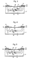
- Fig. 1 shows an embodiment of the invention Diode device with a dynamically optimized diode I, the is formed corresponding to the diode of Fig. 2, and one Protection diode II with high threshold voltage, which corresponds to the 4 is designed.
- the dynamically optimized diode I thus corresponds to the diode of FIG. 2 if the cathode emitter 6 is not used (shown in broken lines in FIG. 1). However, this cathode emitter 6 can also be present in the diode device according to the invention. In this case, the n + -type cathode emitter 6 of FIG. 2 is then provided between the n-type zone 5 and the cathode metallization 8 in addition to FIG. 1.
- the protective diode II in the exemplary embodiment from FIG. 1 can also be constructed corresponding to the diode from FIG. 3 or from FIG. 5. This means that the p + -conducting zone 21 or the n + -conducting layer 22 can also be provided in the layer 19.
- the protection diode II is in the center of the dynamically optimized diode I.
- the dynamically optimized diode I surrounds the protective diode II.
- protection diode II can be dynamic optimized diode I surround.
- the two diodes II and I can be provided in parallel in a strip shape.
- placing the protective diode is particularly advantageous II as close as possible to a later contact point, such as in particular a bond point, because then high peak currents just across a front metallization (Metallization 16) need to flow, but rather directly from this metallization into those that form this diode II Penetrate chip. This will make the Diode device to withstand high surge current peaks as they can occur when switching on devices, significantly improved.
- the dynamically optimized diode I has the usual threshold voltage of a pn junction in silicon of approximately 0.5 ... 0.7 V (cf. pn junction 3) and a comparatively high differential path resistance of approximately 1 ... 10 m ⁇ (in particular 5m ⁇ ) per cm 2 of active chip area.
- This threshold voltage depends on the semiconductor material and has values other than 0.5 ... 0.7 V for SiC, for example.
- the differential path resistance for different current classes and also optimization goals can take on other values.
- platinum for example, it is possible to reduce the lifetime of the charge carriers.
- the p - -conducting zone 2 of the diode I is low doped in comparison to the p + -conducting anode emitter 4, which has a relatively high surface concentration but a low penetration depth.
- the dopant dose of the p + -conducting anode emitter 4 can be between 1.3 x 10 12 dopant atoms cm -2 and 5 x 10 13 dopant atoms cm -2 , in particular between 5 x 10 12 dopant atoms cm -2 and 2 x 10 13 dopant atoms cm -2 .
- the implanted dopant atoms of p-type zone 2 can be diffused out with a diffusion width of approximately 2 ⁇ m.
- the p + -conducting anode emitter can be implanted with a dose of at most 2 x 10 13 dopant atoms cm -2 .
- the p-type zone 2 adjoining the pn junction can be doped with a dose of (1.3 ... 3) x 10 12 dopant atoms cm -2 .
- the protective diode II has a high threshold voltage and a very low differential rail resistance.
- the threshold voltage of the protective diode is significantly higher than that of Band gap of the semiconductor material predetermined threshold voltage, which is about 2.5 V for silicon.
- the Anode emitter i.e. zone 19
- the Threshold voltage is so high that it is only above normal Operating range of the diode II, for example from three to four times the nominal current, a noticeable current flow used in the diode II.
- a suitable threshold voltage Diode II is about 3 ... 5 V.
- the differential path resistance the protective diode II is at least a factor of 5 and preferably a factor 10 lower than the differential Path resistance of diode I.
- an insulating layer 10 made of, for example, silicon dioxide or silicon nitride is provided on the surface of zone 12.
- FIG. 1 shows, similar to FIGS. 3 to 5, an edge insulation layer 14 preferably also made of silicon dioxide or silicon nitride and a polyimide layer 15, which in the edge region is provided on the aluminum metallization 16.
- Boron can be used in the usual way for the p-type dopant be used while a suitable n-type dopant for example, phosphorus.
- the manufacture of the diode device according to the invention only requires a further photo plane to define the p + -conducting zones 4 and 12 and the n + -conducting zone 19 2 and the p + zone 12 and the n + zone 19 are implanted. These implantations can be followed by one or more furnace steps for diffusion of the implanted dopant, especially for zones 12 and 19. A wide out-diffusion is undesirable for the p + -conducting anode emitter 4. In contrast, zones 12 and 19 should be diffused out, since they must prevent direct contact of metallization 16 with the layers underneath, even in the event of small local defects in the implantation.
- the p + -conducting anode emitter 4 is then introduced into the p - -conducting zone 2 by implantation.
- the dose can optionally be chosen so low that the implantation can also be carried out unmasked over the n + -conducting zone 19.
- zones 1, 5 and 6 can therefore be p - , p and p + -conducting and zones 2 and 4 can be n - - and n + -conducting.
- zones 1, 5 and 6 can therefore be p - , p and p + -conducting and zones 2 and 4 can be n - - and n + -conducting.
- zones 1, 5 and 6 can therefore be p - , p and p + -conducting and zones 2 and 4 can be n - - and n + -conducting.
- zones 1, 5 and 6 can therefore be p - , p and p + -conducting and zones 2 and 4 can be n - - and n + -conducting.
Landscapes
- Bipolar Integrated Circuits (AREA)
- Bipolar Transistors (AREA)
- Electrodes Of Semiconductors (AREA)
- Semiconductor Integrated Circuits (AREA)
- Control Of Electrical Variables (AREA)
Abstract
Description
- Fig. 1
- ein Ausführungsbeispiel der erfindungsgemäßen Diodenvorrichtung mit einer dynamisch optimierten Diode I und einer Schutzdiode II mit hoher Schwellspannung;
- Fig. 2
- eine dynamisch optimierte Diode und
- Fig. 3 bis Fig. 5
- verschiedene Beispiele von Schutzdioden.
Claims (20)
- Diodenvorrichtung aus zwei monolithisch miteinander integrierten Dioden (I, II), von denen die eine Diode (I) hinsichtlich ihrer Schalteigenschaften und die andere Diode (II) hinsichtlich ihrer Durchlasseigenschaften im Hochstrombetrieb optimiert sind, wobei die andere Diode (II) erst bei außerhalb des normalen Betriebsbereiches der Diodenvorrichtung liegenden Stromdichten des angelegten Stromes zuschaltet.
dadurch gekennzeichnet, dass die eine Diode (I) eine anodenseitige, schwach dotierte Zone (2) des einen Leitungstyps, eine kathodenseitige, schwach dotierte Driftzone(1) des anderen, zum einen Leitungstyp entgegengesetzten Leitungstyps, die mit der schwach dotierten Zone (2) des einen Leitungstyps einen pn-Übergang (3) bildet, einen an eine Anodenmetallisierung (7) angrenzenden und in der schwach dotierten Zone (2) des einen Leitungstyps vorgesehenen stark dotierten Anodenemitter (4) des einen Leitungstyps und eine Kathodenmetallisierung (8) aufweist, und dass die andere Diode (II) eine in eine schwach dotierte Zone (11) des anderen Leitungstyps eingebettete erste wannenförmige, stark dotierte Zone (12) des einen Leitungstyps und eine in die erste wannenförmige Zone (12) eingebettete zweite wannenförmige, stark dotierte Zone (19) des anderen Leitungstyps aufweist. - Diodenvorrichtung nach Anspruch 1,
dadurch gekennzeichnet, dass der differenzielle Bahnwiderstand der einen Diode (I) 1 ... 10 mΩ, insbesondere 5 mΩ, pro cm2 aktiver Oberfläche eines die Diodenvorrichtung bildenden Chips für eine Sperrspannung von 1200 V beträgt. - Diodenvorrichtung nach Anspruch 1 oder 2,
dadurch gekennzeichnet, dass die Schwellspannung des pn-Übergangs der anderen Diode (II) deutlich über der vom Bandabstand eines für die Diodenvorrichtung verwendeten Halbleitermaterials vorgegebenen Schwellspannung, insbesondere für Silizium 0,5 ... 0,7 V, liegt und 3 ... 5 V beträgt. - Diodenvorrichtung nach einem der Ansprüche 1 bis 3,
dadurch gekennzeichnet, dass der differenzielle Bahnwiderstand der anderen Diode (II) um mindestens einen Faktor 5 und vorzugsweise um einen Faktor 10 niedriger ist als der differenzielle Bahnwiderstand der einen Diode (I). - Diodenvorrichtung nach einem der Ansprüche 1 bis 4,
dadurch gekennzeichnet,dass die schwach dotierte Zone (2) des einen Leitungstyps im Vergleich zu dem eine hohe Oberflächenkonzentration, aber eine geringe Eindringtiefe aufweisenden Anodenemitter (4) niedrig dotiert ist,dass zwischen der Driftzone (1) und der Kathodenmetallisierung (8) eine Zone (5) des anderen Leitungstyps vorgesehen ist,dass die Dotierstoffdosis des Anodenemitters (4) zwischen 1,3 x 10¹² Dotierstoffatomen cm-2 und 5 x 10¹³ Dotierstoffatomen cm-2 liegt, unddass die an den pn-Übergang (3) angrenzende schwach dotierte Zone (2) des einen Leitungstyps mit einer Dosis von (1,3 ... 3) x 1012 Dotierstoffatomen cm-2 dotiert ist. - Diodenvorrichtung nach einem der Ansprüche 1 bis 5,
dadurch gekennzeichnet, dass die Dotierstoffdosis des Anodenemitters (4) zwischen 5 x 10¹² Dotierstoffatomen cm-2 und 2 x 10¹³ Dotierstoffatomen cm-2 liegt. - Diodenvorrichtung nach einem der Ansprüche 1 bis 6,
dadurch gekennzeichnet, dass die implantierten Dotierstoffatome der schwach dotierten Zone (2) des einen Leitungstyps mit einer Diffusionsweite von 2 um ausdiffundiert sind. - Diodenvorrichtung nach einem der Ansprüche 1 bis 7,
dadurch gekennzeichnet, dass der Anodenemitter (4) mit einer Dosis von höchstens 2 x 10¹³ Dotierstoffatomen cm-2 implantiert ist. - Diodenvorrichtung nach einem der Ansprüche 1 bis 8,
dadurch gekennzeichnet, dass der Emitterwirkungsgrad des Anodenemitters (4) durch oberflächennahe Kristallschäden reduziert ist. - Diodenvorrichtung nach einem der Ansprüche 1 bis 9,
dadurch gekennzeichnet, dass in die eine Diode (I) zur Verringerung der Ladungsträger-Lebensdauer durch Diffusion Platin eingebracht ist. - Diodenvorrichtung nach einem der Ansprüche 1 bis 10,
dadurch gekennzeichnet, dass die andere Diode (II) in die eine Diode (I) eingelagert ist. - Diodenvorrichtung nach einem der Ansprüche 1 bis 11,
dadurch gekennzeichnet, dass die andere Diode (II) möglichst nahe an einer Kontaktstelle (vgl. 16) eines äußeren Kontakts gelegen ist. - Diodenvorrichtung nach einem der Ansprüche 1 bis 12,
dadurch gekennzeichnet, dass die Anode der anderen Diode (II) derart gestaltet ist, dass ein im Anodenbereich gebildeter Transistor mit einem Kanal des einen Leitungstyps nicht oder erst bei hohen Stromdichten oberhalb des Sperrstromniveaus des aus der ersten und zweiten wannenförmigen Zone (12, 19) gebildeten pn-Überganges (D2) aufsteuert und bei niedrigen Stromdichten keine Wirkung entfaltet. - Diodenvorrichtung nach einem der Ansprüche 1 bis 13,
dadurch gekennzeichnet, dass Gebiete des anderen Leitungstyps und eine dritte, stark dotierte Zone (21) des einen Leitungstyps so in der zweiten wannenförmigen Zone (19) enthalten sind, dass zwischen der zweiten und dritten Zone (19, 21) ein Emitterkurzschluss vorliegt. - Diodenvorrichtung nach Anspruch 14,
dadurch gekennzeichnet, dass die Anodenmetallisierung (16) zusätzlich zu der dritten Zone (21) auch die zweite wannenförmige Zone (19) kontaktiert. - Diodenvorrichtung nach Anspruch 13,
dadurch gekennzeichnet, dass die Anode aus lediglich der zweiten wannenförmigen Zone (19) gebildet ist. - Diodenvorrichtung nach Anspruch 16,
dadurch gekennzeichnet, dass die zweite wannenförmige Zone (19) einen stark dotierten Kontaktbereich (22) des anderen Leitungstyps enthält. - Diodenvorrichtung nach einem der Ansprüche 1 bis 17,
dadurch gekennzeichnet, dass die erste wannenförmige Zone (12) an ihrer Oberfläche von einer Isolierschicht (10) abgedeckt ist, so dass ein Kurzschluss zwischen dem Anodenemitter (4) und der zweiten wannenförmigen Zone (12) ausgeschlossen ist. - Diodenvorrichtung nach Anspruch 18,
dadurch gekennzeichnet, dass die Driftzone (1) und die Zone (11) des anderen Leitungstyps dasselbe Gebiet sind. - Diodenvorrichtung nach einem der Ansprüche 1 bis 19,
dadurch gekennzeichnet, dass der eine Leitungstyp der p-Leitungstyp ist.
Applications Claiming Priority (2)
| Application Number | Priority Date | Filing Date | Title |
|---|---|---|---|
| DE10046936 | 2000-09-21 | ||
| DE10046936A DE10046936A1 (de) | 2000-09-21 | 2000-09-21 | Diodenvorrichtung aus zwei monolithisch miteinander integrierten Dioden |
Publications (3)
| Publication Number | Publication Date |
|---|---|
| EP1191594A2 true EP1191594A2 (de) | 2002-03-27 |
| EP1191594A3 EP1191594A3 (de) | 2004-11-24 |
| EP1191594B1 EP1191594B1 (de) | 2006-12-27 |
Family
ID=7657194
Family Applications (1)
| Application Number | Title | Priority Date | Filing Date |
|---|---|---|---|
| EP01121302A Expired - Lifetime EP1191594B1 (de) | 2000-09-21 | 2001-09-05 | Diodenvorrichtung aus zwei monolithisch miteinander integrierten Dioden |
Country Status (2)
| Country | Link |
|---|---|
| EP (1) | EP1191594B1 (de) |
| DE (2) | DE10046936A1 (de) |
Cited By (1)
| Publication number | Priority date | Publication date | Assignee | Title |
|---|---|---|---|---|
| WO2006029921A1 (de) * | 2004-09-13 | 2006-03-23 | Robert Bosch Gmbh | Halbleiteranordnung zur spannungsbegrenzung |
Family Cites Families (8)
| Publication number | Priority date | Publication date | Assignee | Title |
|---|---|---|---|---|
| US4017882A (en) * | 1975-12-15 | 1977-04-12 | Rca Corporation | Transistor having integrated protection |
| FR2458146A1 (fr) * | 1979-05-29 | 1980-12-26 | Thomson Csf | Structure integree comportant un transistor et trois diodes antisaturation |
| DE3633161A1 (de) * | 1986-09-30 | 1988-04-07 | Licentia Gmbh | Halbleiterbauelement mit einer anodenseitigen p-zone und einer anliegenden schwach dotierten n-basiszone |
| DE4135259C1 (de) * | 1991-10-25 | 1993-01-07 | Semikron Elektronik Gmbh, 8500 Nuernberg, De | |
| JPH06314801A (ja) * | 1993-03-05 | 1994-11-08 | Mitsubishi Electric Corp | 半導体装置およびその製造方法 |
| US5969400A (en) * | 1995-03-15 | 1999-10-19 | Kabushiki Kaisha Toshiba | High withstand voltage semiconductor device |
| DE19543922A1 (de) * | 1995-11-24 | 1997-05-28 | Siemens Ag | Verfahren zum Herabsetzen der Trägerspeicherladung in Halbleiterbauelementen |
| JPH09321321A (ja) * | 1996-05-28 | 1997-12-12 | Fuji Electric Co Ltd | 電力用ダイオード |
-
2000
- 2000-09-21 DE DE10046936A patent/DE10046936A1/de not_active Withdrawn
-
2001
- 2001-09-05 DE DE50111719T patent/DE50111719D1/de not_active Expired - Lifetime
- 2001-09-05 EP EP01121302A patent/EP1191594B1/de not_active Expired - Lifetime
Cited By (3)
| Publication number | Priority date | Publication date | Assignee | Title |
|---|---|---|---|---|
| WO2006029921A1 (de) * | 2004-09-13 | 2006-03-23 | Robert Bosch Gmbh | Halbleiteranordnung zur spannungsbegrenzung |
| US7671379B2 (en) | 2004-09-13 | 2010-03-02 | Robert Bosch Gmbh | Semiconductor system for voltage limitation |
| CN101019238B (zh) * | 2004-09-13 | 2010-06-02 | 罗伯特·博世有限公司 | 用于电压限制的半导体结构 |
Also Published As
| Publication number | Publication date |
|---|---|
| EP1191594B1 (de) | 2006-12-27 |
| EP1191594A3 (de) | 2004-11-24 |
| DE10046936A1 (de) | 2002-04-18 |
| DE50111719D1 (de) | 2007-02-08 |
Similar Documents
| Publication | Publication Date | Title |
|---|---|---|
| DE3519389C2 (de) | ||
| DE19811297B4 (de) | MOS-Halbleitervorrichtung mit hoher Durchbruchspannung | |
| DE10361136B4 (de) | Halbleiterdiode und IGBT | |
| DE102006050338B4 (de) | Halbleiterbauelement mit verbessertem Speicherladung zu Dioden-Softness Trade-off | |
| DE69305909T2 (de) | Leistungsanordnung mit isoliertem Gate-Kontakt-Gebiet | |
| EP0283496B1 (de) | Halbleiterbauelement mit einer anodenseitigen p-zone und einer anliegenden schwach dotierten n-basiszone | |
| DE3008034A1 (de) | Elektrodenvorrichtung fuer eine halbleitervorrichtung | |
| DE3856150T2 (de) | Halbleiteranordnung und verfahren zur herstellung | |
| DE68923789T2 (de) | Optische halbleitervorrichtung mit einer nulldurchgangsfunktion. | |
| EP0623960B1 (de) | IGBT mit mindestens zwei gegenüberliegenden Kanalgebieten pro Sourcegebiet und Verfahren zu dessen Herstellung | |
| DE69938418T2 (de) | Graben-gate-halbleiteranordnung | |
| EP0913000B1 (de) | Durch feldeffekt steuerbares halbleiterbauelement | |
| DE19528998C2 (de) | Bidirektionaler Halbleiterschalter und Verfahren zu seiner Steuerung | |
| DE10031461B4 (de) | Hochvolt-Diode | |
| DE102004017723A1 (de) | In Rückwärtsrichtung sperrendes Halbleiterbauteil und Verfahren zu seiner Herstellung | |
| EP0710988B1 (de) | Verfahren zum Herstellen von durch Feldeffekt steuerbaren Halbleiterbauelementen | |
| DE10203820A1 (de) | Halbleiterbauelement und Verfahren zu dessen Herstellung | |
| DE3010986A1 (de) | Integrierte halbleiterschaltung | |
| DE4006886C2 (de) | ||
| EP0017980A1 (de) | Thyristor mit Steuerung durch Feldeffekttransistor | |
| DE69318346T2 (de) | Schutzdiode für ein vertikales Halbleiterbauelement | |
| EP1191594B1 (de) | Diodenvorrichtung aus zwei monolithisch miteinander integrierten Dioden | |
| DE10126309A1 (de) | Rückwärtssperrendes Leistungshalbleiterbauelement | |
| DE3632642A1 (de) | Halbleiter-leistungs-bauelement | |
| DE2909795A1 (de) | Halbleiter-schaltvorrichtung |
Legal Events
| Date | Code | Title | Description |
|---|---|---|---|
| PUAI | Public reference made under article 153(3) epc to a published international application that has entered the european phase |
Free format text: ORIGINAL CODE: 0009012 |
|
| AK | Designated contracting states |
Kind code of ref document: A2 Designated state(s): AT BE CH CY DE DK ES FI FR GB GR IE IT LI LU MC NL PT SE TR |
|
| AX | Request for extension of the european patent |
Free format text: AL;LT;LV;MK;RO;SI |
|
| PUAL | Search report despatched |
Free format text: ORIGINAL CODE: 0009013 |
|
| AK | Designated contracting states |
Kind code of ref document: A3 Designated state(s): AT BE CH CY DE DK ES FI FR GB GR IE IT LI LU MC NL PT SE TR |
|
| AX | Request for extension of the european patent |
Extension state: AL LT LV MK RO SI |
|
| 17P | Request for examination filed |
Effective date: 20050520 |
|
| AKX | Designation fees paid |
Designated state(s): DE FR GB IT |
|
| GRAP | Despatch of communication of intention to grant a patent |
Free format text: ORIGINAL CODE: EPIDOSNIGR1 |
|
| RIN1 | Information on inventor provided before grant (corrected) |
Inventor name: RUPP, ROLAND, DR. Inventor name: KAPELS, HOLGER Inventor name: GRIEBL, ERICH, DR. Inventor name: WILLMEROTH, ARMIN Inventor name: MAUDER, ANTON, DR. |
|
| GRAS | Grant fee paid |
Free format text: ORIGINAL CODE: EPIDOSNIGR3 |
|
| GRAA | (expected) grant |
Free format text: ORIGINAL CODE: 0009210 |
|
| AK | Designated contracting states |
Kind code of ref document: B1 Designated state(s): DE FR GB IT |
|
| REG | Reference to a national code |
Ref country code: GB Ref legal event code: FG4D Free format text: NOT ENGLISH |
|
| REF | Corresponds to: |
Ref document number: 50111719 Country of ref document: DE Date of ref document: 20070208 Kind code of ref document: P |
|
| GBT | Gb: translation of ep patent filed (gb section 77(6)(a)/1977) |
Effective date: 20070516 |
|
| ET | Fr: translation filed | ||
| PLBE | No opposition filed within time limit |
Free format text: ORIGINAL CODE: 0009261 |
|
| STAA | Information on the status of an ep patent application or granted ep patent |
Free format text: STATUS: NO OPPOSITION FILED WITHIN TIME LIMIT |
|
| 26N | No opposition filed |
Effective date: 20070928 |
|
| REG | Reference to a national code |
Ref country code: FR Ref legal event code: PLFP Year of fee payment: 16 |
|
| REG | Reference to a national code |
Ref country code: FR Ref legal event code: PLFP Year of fee payment: 17 |
|
| PGFP | Annual fee paid to national office [announced via postgrant information from national office to epo] |
Ref country code: IT Payment date: 20170926 Year of fee payment: 17 Ref country code: GB Payment date: 20170921 Year of fee payment: 17 Ref country code: FR Payment date: 20170928 Year of fee payment: 17 |
|
| PGFP | Annual fee paid to national office [announced via postgrant information from national office to epo] |
Ref country code: DE Payment date: 20171129 Year of fee payment: 17 |
|
| REG | Reference to a national code |
Ref country code: DE Ref legal event code: R119 Ref document number: 50111719 Country of ref document: DE |
|
| GBPC | Gb: european patent ceased through non-payment of renewal fee |
Effective date: 20180905 |
|
| PG25 | Lapsed in a contracting state [announced via postgrant information from national office to epo] |
Ref country code: IT Free format text: LAPSE BECAUSE OF NON-PAYMENT OF DUE FEES Effective date: 20180905 Ref country code: DE Free format text: LAPSE BECAUSE OF NON-PAYMENT OF DUE FEES Effective date: 20190402 |
|
| PG25 | Lapsed in a contracting state [announced via postgrant information from national office to epo] |
Ref country code: FR Free format text: LAPSE BECAUSE OF NON-PAYMENT OF DUE FEES Effective date: 20180930 |
|
| PG25 | Lapsed in a contracting state [announced via postgrant information from national office to epo] |
Ref country code: GB Free format text: LAPSE BECAUSE OF NON-PAYMENT OF DUE FEES Effective date: 20180905 |