EP1189084A2 - Planar lightwave circuit and optical circuit - Google Patents
Planar lightwave circuit and optical circuit Download PDFInfo
- Publication number
- EP1189084A2 EP1189084A2 EP01307672A EP01307672A EP1189084A2 EP 1189084 A2 EP1189084 A2 EP 1189084A2 EP 01307672 A EP01307672 A EP 01307672A EP 01307672 A EP01307672 A EP 01307672A EP 1189084 A2 EP1189084 A2 EP 1189084A2
- Authority
- EP
- European Patent Office
- Prior art keywords
- waveguide
- core width
- substrate
- core
- input
- Prior art date
- Legal status (The legal status is an assumption and is not a legal conclusion. Google has not performed a legal analysis and makes no representation as to the accuracy of the status listed.)
- Granted
Links
Images












Classifications
-
- G—PHYSICS
- G02—OPTICS
- G02B—OPTICAL ELEMENTS, SYSTEMS OR APPARATUS
- G02B6/00—Light guides; Structural details of arrangements comprising light guides and other optical elements, e.g. couplings
- G02B6/10—Light guides; Structural details of arrangements comprising light guides and other optical elements, e.g. couplings of the optical waveguide type
- G02B6/12—Light guides; Structural details of arrangements comprising light guides and other optical elements, e.g. couplings of the optical waveguide type of the integrated circuit kind
- G02B6/12007—Light guides; Structural details of arrangements comprising light guides and other optical elements, e.g. couplings of the optical waveguide type of the integrated circuit kind forming wavelength selective elements, e.g. multiplexer, demultiplexer
- G02B6/12009—Light guides; Structural details of arrangements comprising light guides and other optical elements, e.g. couplings of the optical waveguide type of the integrated circuit kind forming wavelength selective elements, e.g. multiplexer, demultiplexer comprising arrayed waveguide grating [AWG] devices, i.e. with a phased array of waveguides
- G02B6/12011—Light guides; Structural details of arrangements comprising light guides and other optical elements, e.g. couplings of the optical waveguide type of the integrated circuit kind forming wavelength selective elements, e.g. multiplexer, demultiplexer comprising arrayed waveguide grating [AWG] devices, i.e. with a phased array of waveguides characterised by the arrayed waveguides, e.g. comprising a filled groove in the array section
-
- G—PHYSICS
- G02—OPTICS
- G02B—OPTICAL ELEMENTS, SYSTEMS OR APPARATUS
- G02B6/00—Light guides; Structural details of arrangements comprising light guides and other optical elements, e.g. couplings
- G02B6/10—Light guides; Structural details of arrangements comprising light guides and other optical elements, e.g. couplings of the optical waveguide type
- G02B6/12—Light guides; Structural details of arrangements comprising light guides and other optical elements, e.g. couplings of the optical waveguide type of the integrated circuit kind
- G02B6/12007—Light guides; Structural details of arrangements comprising light guides and other optical elements, e.g. couplings of the optical waveguide type of the integrated circuit kind forming wavelength selective elements, e.g. multiplexer, demultiplexer
- G02B6/12009—Light guides; Structural details of arrangements comprising light guides and other optical elements, e.g. couplings of the optical waveguide type of the integrated circuit kind forming wavelength selective elements, e.g. multiplexer, demultiplexer comprising arrayed waveguide grating [AWG] devices, i.e. with a phased array of waveguides
- G02B6/12016—Light guides; Structural details of arrangements comprising light guides and other optical elements, e.g. couplings of the optical waveguide type of the integrated circuit kind forming wavelength selective elements, e.g. multiplexer, demultiplexer comprising arrayed waveguide grating [AWG] devices, i.e. with a phased array of waveguides characterised by the input or output waveguides, e.g. tapered waveguide ends, coupled together pairs of output waveguides
-
- G—PHYSICS
- G02—OPTICS
- G02B—OPTICAL ELEMENTS, SYSTEMS OR APPARATUS
- G02B6/00—Light guides; Structural details of arrangements comprising light guides and other optical elements, e.g. couplings
- G02B6/10—Light guides; Structural details of arrangements comprising light guides and other optical elements, e.g. couplings of the optical waveguide type
- G02B6/12—Light guides; Structural details of arrangements comprising light guides and other optical elements, e.g. couplings of the optical waveguide type of the integrated circuit kind
- G02B6/12007—Light guides; Structural details of arrangements comprising light guides and other optical elements, e.g. couplings of the optical waveguide type of the integrated circuit kind forming wavelength selective elements, e.g. multiplexer, demultiplexer
- G02B6/12009—Light guides; Structural details of arrangements comprising light guides and other optical elements, e.g. couplings of the optical waveguide type of the integrated circuit kind forming wavelength selective elements, e.g. multiplexer, demultiplexer comprising arrayed waveguide grating [AWG] devices, i.e. with a phased array of waveguides
- G02B6/12023—Light guides; Structural details of arrangements comprising light guides and other optical elements, e.g. couplings of the optical waveguide type of the integrated circuit kind forming wavelength selective elements, e.g. multiplexer, demultiplexer comprising arrayed waveguide grating [AWG] devices, i.e. with a phased array of waveguides characterised by means for reducing the polarisation dependence, e.g. reduced birefringence
-
- G—PHYSICS
- G02—OPTICS
- G02B—OPTICAL ELEMENTS, SYSTEMS OR APPARATUS
- G02B6/00—Light guides; Structural details of arrangements comprising light guides and other optical elements, e.g. couplings
- G02B6/10—Light guides; Structural details of arrangements comprising light guides and other optical elements, e.g. couplings of the optical waveguide type
- G02B6/12—Light guides; Structural details of arrangements comprising light guides and other optical elements, e.g. couplings of the optical waveguide type of the integrated circuit kind
- G02B6/122—Basic optical elements, e.g. light-guiding paths
- G02B6/1228—Tapered waveguides, e.g. integrated spot-size transformers
-
- G—PHYSICS
- G02—OPTICS
- G02B—OPTICAL ELEMENTS, SYSTEMS OR APPARATUS
- G02B6/00—Light guides; Structural details of arrangements comprising light guides and other optical elements, e.g. couplings
- G02B6/10—Light guides; Structural details of arrangements comprising light guides and other optical elements, e.g. couplings of the optical waveguide type
- G02B6/12—Light guides; Structural details of arrangements comprising light guides and other optical elements, e.g. couplings of the optical waveguide type of the integrated circuit kind
- G02B6/13—Integrated optical circuits characterised by the manufacturing method
- G02B6/132—Integrated optical circuits characterised by the manufacturing method by deposition of thin films
-
- G—PHYSICS
- G02—OPTICS
- G02B—OPTICAL ELEMENTS, SYSTEMS OR APPARATUS
- G02B6/00—Light guides; Structural details of arrangements comprising light guides and other optical elements, e.g. couplings
- G02B6/10—Light guides; Structural details of arrangements comprising light guides and other optical elements, e.g. couplings of the optical waveguide type
- G02B6/12—Light guides; Structural details of arrangements comprising light guides and other optical elements, e.g. couplings of the optical waveguide type of the integrated circuit kind
- G02B6/13—Integrated optical circuits characterised by the manufacturing method
- G02B6/136—Integrated optical circuits characterised by the manufacturing method by etching
-
- G—PHYSICS
- G02—OPTICS
- G02B—OPTICAL ELEMENTS, SYSTEMS OR APPARATUS
- G02B6/00—Light guides; Structural details of arrangements comprising light guides and other optical elements, e.g. couplings
- G02B6/10—Light guides; Structural details of arrangements comprising light guides and other optical elements, e.g. couplings of the optical waveguide type
- G02B6/12—Light guides; Structural details of arrangements comprising light guides and other optical elements, e.g. couplings of the optical waveguide type of the integrated circuit kind
- G02B2006/12083—Constructional arrangements
- G02B2006/121—Channel; buried or the like
-
- G—PHYSICS
- G02—OPTICS
- G02B—OPTICAL ELEMENTS, SYSTEMS OR APPARATUS
- G02B6/00—Light guides; Structural details of arrangements comprising light guides and other optical elements, e.g. couplings
- G02B6/10—Light guides; Structural details of arrangements comprising light guides and other optical elements, e.g. couplings of the optical waveguide type
- G02B6/12—Light guides; Structural details of arrangements comprising light guides and other optical elements, e.g. couplings of the optical waveguide type of the integrated circuit kind
- G02B2006/12166—Manufacturing methods
- G02B2006/12176—Etching
Definitions
- the present invention relates to a planar lightwave circuit (PLC) which can decrease the coupling loss between a planar lightwave circuit and an optical fiber or between planar lightwave circuits.
- PLC planar lightwave circuit
- planar lightwave circuits will be used more and more as main parts which have important functions such as routing of an optical signal in superfast large-capacity optical communication systems from now on. Especially, it is required to construct a larger optical communication system as capacity required for communication increases. In order to realize the enlargement of the optical communication system, it is necessary to downsize the planar lightwave circuit and to allow connection between many planar lightwave circuits.
- Fig.1 is a schematic diagram of structure of a conventional planar lightwave circuit.
- an input waveguide 112 is formed on a substrate 111.
- the input waveguide 112 is connected to a slab waveguide 113 formed on the substrate 111.
- One end of a plurality of arrayed waveguides 114 formed on the substrate 111 is connected to the slab waveguide 113.
- a half waveplate 115 which gets rid of polarization dependence is provided at some midpoint of the arrayed waveguides 114.
- the other end of the arrayed waveguides 114 is connected to a slab waveguide 116 formed on the substrate 111.
- a plurality of output waveguides formed on the substrate 111 are connected to the slab waveguide 116.
- the optical signal When an optical signal is entered into the planar lightwave circuit 110 from the input waveguide 112, the optical signal is entered into the arrayed waveguides 114 via the slab waveguide 113 and polarization dependence is dissolved by the half waveplate 115.
- the optical signal is demultiplexed into signals of various wavelengths in the slab waveguide 116 due to delay line of the arrayed waveguides 114 so that demultiplexed signals are output from the output waveguides 117.
- relative refractive index difference is a high value which is larger than 1%
- relative refractive index difference is the ratio of difference between the refractive index n core of the core and refractive index n clad of the cladding to the refractive index n core of the core as represented by the following equation (1).
- the coupling loss occurs when connecting different types of waveguides.
- the coupling loss occurs due to difference of field distribution between the different types of waveguides, and the coupling loss accumulates as connecting points increases. For example, as for 1.5 ⁇ m wavelength which is used in an optical communication system, large coupling loss about 3.5dB occurs between a single-mode optical fiber of core diameter 9 ⁇ m and a superhigh- waveguide about 5 ⁇ m per side.
- planar lightwave circuit 110 used in the optical communication system downsizing and decreasing of the coupling loss are mutually contradictory. That is, although the circuit can be downsized by increasing , the coupling loss increases. Therefore, construction of a practical system has limitations. That is, it becomes difficult to enlarge capacity of transmission lines unless the coupling loss of the superhigh- waveguide is decreased, so that functions and scale of the optical communication system may be limited.
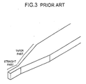
- a spotsize converter in which core width is narrowed toward an end face of a substrate is known as shown in Fig.3 (for example, Japanese laid-open patent application No.63-280202).
- a planar lightwave circuit in which an input waveguide and an output waveguide are formed on a substrate wherein each of the input waveguide and the output waveguide are formed by a core and a cladding which covers the core, and refractive index of the core is higher than refractive index of the cladding, wherein:
- a taper part is formed in the core in each of the input end side of the input waveguide and the output end side of the output waveguide, and a taper angle of the taper part is larger than 0° and equal to or smaller than 5° .
- steps are formed in the core in each of the input end side of the input waveguide and the output end side of the output waveguide.
- height between adjacent steps in the steps is larger than 0 ⁇ m and equal to or smaller than 5 ⁇ m.
- taper parts and straight parts are formed alternately in the core in each of the input end side of the input waveguide and the output end side of the output waveguide, core width of each of the taper parts changes gradually toward an end face of the substrate and core width of each of the straight parts is constant.
- length of each of the straight parts is equal to or larger than 1 ⁇ m.
- a marker is provided for indicating a cutting position of the input waveguide or the output waveguide, or indicating a position where the core width changes.
- the planar lightwave circuit may include a monitor waveguide in which an input end of the monitor waveguide is formed in an end face side of the substrate which is different from end face sides in which the input end of the input waveguide and the output end of the output waveguide are provided, wherein the monitor waveguide includes a core which is formed such that core width changes toward an end face of the substrate.
- planar lightwave circuit may include a monitor waveguide, wherein an input end of the monitor waveguide is formed in an end face side of the substrate in which the input end of the input waveguide is located, and
- the substrate is made of silicon and the input waveguide and the output waveguide are made of silica-based glass.
- an optical circuit which includes a waveguide and a spotsize converter which is a part of the waveguide, wherein a core is embedded in a cladding in the waveguide, and the spotsize converter is located near an end face of a substrate on which the optical circuit is formed, the spotsize converter including:
- an optimized taper is used as a shape of the taper part.
- an optical circuit which includes a waveguide and a spotsize converter which is a part of the waveguide, wherein a core is embedded in a cladding in the waveguide, and the spotsize converter is located near an end face of a substrate on which the optical circuit is formed, the spotsize converter including:
- a length of the straight part is equal to or larger than 1 ⁇ m.
- a mean taper angle of the spotsize converter is larger than 0° and equal to or smaller than 5°.
- an optical circuit which includes a waveguide and a spotsize converter which is a part of the waveguide, wherein a core is embedded in a cladding in the waveguide, and the spotsize converter is located near an end face of a substrate on which the optical circuit is formed, the spotsize converter including:
- the core width fine-tuning part may include a plurality of taper parts.
- the core width fine-tuning part may include alternating taper parts and straight parts, core width of each straight part being constant.
- the core width fine-tuning part may include;
- an optimized taper is used as a shape of the core width converting part.
- a mean taper angle ⁇ 1 of the core width fine-tuning part is larger than 0° and equal to or smaller than 0.04°
- a mean taper angle ⁇ 2 of the core width converting part is larger than 0.04° and equal to or smaller than 5° .
- a marker for forming an end face of the substrate is provided in the optical circuit.
- the marker is provided in a location corresponding to a location in which a shape of the core width fine-tuning part changes.
- a monitor waveguide is provided on the substrate, the monitor waveguide including a second spotsize converter including:
- the optical circuit includes a plurality of the monitor waveguides, spotsize converters of the monitor waveguides are shifted to each other by a predetermined distance in the direction of the length of the monitor waveguides.
- the optical circuit may include a first monitor waveguide and a second monitor waveguide;
- an optical circuit which includes input ports and output ports, each of the input ports and the output ports including:
- the spotsize converter which uses the narrow taper
- fabrication tolerance of core width is very narrow for minimizing the coupling loss between the planar lightwave circuit and the optical fiber. That is, an optimum value of the core width changes due to fabrication conditions of the relative refractive index difference between the core and the cladding, core thickness and the like.
- the core width of the input waveguide is narrowed toward the end face of the substrate to allow the core width to be fine-tuned so that the optimum core width can be obtained. By adjusting the position of the end face, the optimum core width can be obtained with high reproducibility
- Fig.4 is a schematic block diagram of the planar lightwave circuit
- Fig.5 is a magnified view of the core of the input waveguide and the output waveguide of the planar lightwave circuit of Fig.4.
- Figs.6A - 6E are diagrams for explaining a process for fabricating the input waveguide and the output waveguide of the planar lightwave circuit of Fig.4.
- Fig.7 shows a relationship between the core width and the coupling loss of the end face of the substrate which is obtained by calculation.
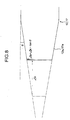
- Fig.8 is a diagram for explaining dicing error.
- an input waveguide 12 made of silica-based glass is formed on a substrate 11 made of silicon in which the input waveguide 12 includes a core having high refractive index and a cladding having low refractive index, and the core is covered by the cladding.
- the core 12a of the input waveguide 12 has a taper part 12aa in which the core width decreases gradually toward the input end which is located in the end face side of the substrate 11.
- the part of the waveguide in which the core width decreases gradually from a part near the end face of the substrate toward the end face of the substrate will be called a spotsize converter.
- the taper part shown in Fig.5 is a spotsize converter.
- the input waveguide 12 is connected to a slab waveguide 13 made of silica-based glass.
- Each one end of arrayed waveguide 14 made of silica-based glass formed on the substrate 11 is connected to the slab waveguide 13.
- a half waveplate 15 for dissolving polarization dependence is provided at some midpoint of the arrayed waveguides 14.
- the other ends of the arrayed waveguides 14 are connected to a slab waveguide 16 made of silica-based glass formed on the substrate 11.
- Output waveguides 17 made of silica-based glass formed on the substrate 11 are connected to the slab waveguide 16.
- the core 17a of the output waveguide 17 has a taper part 17aa in which the core width decreases gradually toward the output end which is located in another end face side of the substrate 11 as shown in Fig.5.
- the waveguide 12, 17 of the planar lightwave circuit can be fabricated in the following way.
- undercladding glass soot mainly made of SiO 2 is deposited on the substrate 11 made of silicon by a flame hydrolysis deposition (FHD) method.
- core glass soot in which GeO 2 is doped to SiO 2 is deposited on the undercladding glass soot by the flame hydrolysis deposition method.
- high temperature heat-treatment larger than 1000°C
- high temperature heat-treatment is carried out for the glass soot such that the glass soot becomes transparent.
- an undercladding glass 12ba and a core glass 12a are formed on the substrate 11 (Fig.6A). Thickness is adjusted such that thickness of the undercladding glass 12ba and the core glass 12a become proper when depositing the glass soot by the flame hydrolysis deposition method.
- etching masks 100 are formed on the core glass 12a using photolithography such that each etching mask 100 becomes tapered structure, that is, width of each etching mask 100 decreases toward the end face of the substrate 11 (Fig.6B). After that, patterning of the core glass 12a is performed (Fig.6C), and the etching masks 100 are removed (Fig.6D).
- overcladding glass 12bb mainly made of SiO 2 is deposited on the undercladding glass 12ba and the core glass 12a by the flame hydrolysis deposition method so that the overcladding glass 12bb also spreads into a narrow spacing between the adjacent core glasses, wherein dopant such as B 2 O 3 and P 2 O 5 is doped in the overcladding glass 12ba so that glass transition temperature is lowered (Fig.6E). Then, the waveguide 12, 17 can be formed on the substrate 11.
- the optical signal in which lights of a plurality of different wavelengths are multiplexed is entered in the input waveguide 12
- the optical signal is entered in the arrayed waveguides 14 via the slab waveguide 13, and polarization dependence is dissolved by the half waveplate 15.
- the optical signal is demultiplexed into optical signals of the wavelengths in the slab waveguide 16 due to delay line of the arrayed waveguides 14. Then, the optical signals are output from the output waveguides 17.
- Fig.7 shows a relationship between the core width at the end face of the substrate and the coupling loss which is calculated for a single-mode optical fiber of 9 ⁇ m core diameter, in which the core thickness is 5 ⁇ m and is 1.5%.
- the core width is decreased gradually from 5 ⁇ m, the spotsize in the waveguide decreases so that the coupling loss increases.
- the core width becomes smaller than 4 ⁇ m, confinement of light into the core becomes weak and the spotsize is widened so that the coupling loss becomes lowered.
- the coupling loss becomes minimum at core width close to 1.2 ⁇ m.
- the coupling loss increases rapidly as the core width decreases below 1.2 ⁇ m. This is because the spotsize rapidly increases since the core width is too narrow.
- the coupling loss reaches its minimum value of approximately 0.5dB.
- the coupling loss can be suppressed to about 1.0dB in total of both ends of input and output. Since the waveguide is designed such that a single-mode light propagates, width and thickness of the core of the waveguide are determined by the material and the like.
- the taper part 12aa, 17aa is provided in the core 12a, 17a of the waveguide 12, 17 at the end face side of the substrate 11 in the planar lightwave circuit 10 of the first example in this embodiment. Accordingly, the coupling loss is decreased while satisfying propagation conditions of the single-mode light.
- the coupling loss increases rapidly when the core width deviates from 1.2 ⁇ m even slightly.
- the coupling loss may increase due to deviation from optimum width caused by dicing error of the planar lightwave circuit 10.
- deviation amount of one side of the core width can be represented by the following equation (2).
- the coupling loss becomes about 0.7dB, which means that the coupling loss is only about 0.2dB larger than that when x is 0.
- the taper angle ⁇ of the taper part 12aa, 17aa of the core 12a, 17a of the waveguide 12, 17 is larger than 0° and equal to or smaller than 5° . Because, if the taper angle ⁇ is 0° , the effect of the present invention can not be obtained, and, if the taper angle is larger than 5° , the deviation amount a of the core width due to dicing error becomes too large so that the coupling loss becomes too large.
- silica-based waveguides 11 ⁇ 17 are formed on the silicon substrate 11.
- materials are not limited to these.
- the waveguides 11 ⁇ 17 which are made of polyimide, silicon, semiconductor, LiNbO 3 and the like can be formed on the substrate 11 which is made of various materials.
- a core 32a, 37a shown in Fig.9 can be provided for example.
- a plurality of steps 32aa, 37aa are provided such that the core width becomes smaller toward the input end or the output end which is located at the end face side of the substrate 11.
- the steps 32aa, 37aa are provided as many as possible in consideration of the dicing error x.
- the waveguide when low coupling loss can not be obtained at a dicing position, the waveguide can be used after cutting the substrate at a different position, since the core width becomes smaller toward the input end or the output end by using the steps 32aa, 37aa. Therefore, even when an accurate optimum core width is not known and only an estimated value of an analytic result is obtained, the optimum core width can be searched for by changing the cutting position.
- the height difference between the adjacent steps b is larger than 0 ⁇ m and equal to or smaller than 5 ⁇ m, Because, when b is equal to 0 ⁇ m, the effect of the present invention can not be obtained. When b exceeds 5 ⁇ m, the propagation condition of the single-mode light can not be satisfied.
- the height b and the length of the step are fixed for each step.
- the height b and the length of the step may be formed different for each step.
- a core 42a, 47a can be used.
- alternating taper parts 42aa, 47aa and straight parts 42ab, 47ab are provided at the input end side or the output end side located in the end face side of the substrate 11, wherein the core width becomes smaller toward the input or output end as for the taper part, and the core width is fixed at a constant width as for the straight part which is formed along the axis of the core.
- the coupling loss can be decreased while the propagation condition of the single-mode light is satisfied.
- the dicing error can be absorbed by cutting the substrate at the straight part 42ab, 47ab. Therefore, a proper core width can be realized easily.
- the length s of the straight part 42ab, 47ab is equal to or larger than 1 ⁇ m. Because, when s is smaller than 1 ⁇ m, it becomes difficult to absorb dicing error.
- markers La1, La2 which indicate dicing positions may be formed near the input or output end of 'the waveguide of the planar lightwave circuit 10 when fabricating the planar lightwave circuit 10.
- markers Lb1, Lb2 which indicate changing positions of core width may be provided, By providing these markers, the accuracy of dicing can be easily improved.
- Fig.12 shows a schematic block diagram of the planar lightwave circuit
- Fig.13 shows a magnified view of the core of the input waveguides or the output waveguides. Parts which are the same as those of the first embodiment are not described, and the same symbols as those used in the first embodiment are used.
- the present invention is applied to an arrayed waveguide grating (AWG), which is one of planar lightwave circuits, which performs multiplexing of optical signals of a plurality of different wavelengths and demultiplexing in an wavelength division multiplexing communication system.
- AWG is an example of a waveguide type optical circuit.
- a plurality of input waveguides 12 are provided on the substrate 11.
- the core width of input end face of the taper part 12aa of the core 12a is different by each input waveguide as shown in Fig.13.
- a plurality of output waveguides 17 are provided on the substrate 11.
- the core width of input end face of the taper part 17aa of the core 17a is different by each output waveguide as shown in Fig.13.
- the waveguide 12, 17 of the AWG 50 can be fabricated in the same way as the planar lightwave circuit 10 in the first embodiment basically.
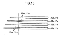
- etching masks of taper shape are formed, wherein the width of each etching mask becomes smaller toward the end of the substrate, and the taper angle ⁇ of the etching masks is different from each other.
- etching masks which have the same taper angle may be provided in which the position of the spotsize converters are shifted in the horizontal direction. Then, reactive ion etching is performed and the substrate is cut straightly. Accordingly, the cores 12a, 17a which include taper parts 12aa, 17aa in which the core width is different from each other can be easily formed.
- the AWG 50 which has such structure, when an optical signal in which lights of a plurality of different wavelengths are multiplexed is entered in any one of input waveguides 12, the optical signal is entered in the arrayed waveguides 14 via the slab waveguide 13, and polarization dependence is dissolved by the half waveplate 15. In addition, the optical signal is demultiplexed into optical signals of the wavelengths in the slab waveguide 16 due to delay line of the arrayed waveguides 14. Then, the optical signals are output from the output waveguides 17.
- the multiplexed optical signal entered from an input port (which is not shown in the figure) which is connected to the input waveguide 12 is demultiplexed into signals having different wavelengths and the demultiplexed signals are output from output ports (which is not shown in the figure) connected to the output waveguides 17.
- the coupling loss varies from output port to output port since the core width varies from output port to output port due to dicing error.
- the core 42a, 47a of the third example of the first embodiment in which alternating taper parts 42aa, 47aa and straight parts 42ab, 47ab are provided at the input end side or the output end side located in the end face side of the substrate 11, wherein the core width becomes smaller toward the input or output end as for the taper part, and the core width is fixed at a constant width as for the straight part which is formed along the axis of the core.
- an input port is selected among input ports connected to the input waveguides 12 such that the coupling loss becomes smallest.
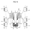
- the optical circuit shown in Fig.16 includes AWG 50, input ports i and output ports j.
- the input port i includes a plurality of input waveguides which were described in the first embodiment and each input port is connected to an input waveguide 12 of AWG 50.
- the output port j includes a plurality of the output waveguides which were described in the first embodiment and each output waveguide is connected to an output waveguide 17 of the AWG 50.
- each input port i an input waveguide is selected so that signal light is input to an input waveguide 12 of AWG 50, and the signal light is output from output waveguides of the output port j connected to an output waveguide 17 of the AWG 50. Therefore, the coupling loss can be decreased in every port i, j regardless of fabrication error.
- Fig.17 is a schematic block diagram of the planar lightwave circuit. Parts which are the same as those of the first and second embodiments will not be described, and the same symbols as those used in the first and second embodiments will be used.
- first monitor waveguides 68 and second monitor waveguides 69 are provided on the substrate 11.
- input ends 68a are located in an end face side of the substrate 11 other than end face sides where the input ends and output ends of the input waveguides 12 and output waveguides 17 are located.
- the input end side of the first monitor waveguide is formed as taper such that the core width is decreased toward the input end.
- the core widths of the input ends 68a are different from each other.
- the output ends 68b are located in the end face side of the substrate 11 where the output ends of the output waveguides 17 are located.
- the second monitor waveguides 69 structures of the input ends 69a and the output ends 69b are the same as those of the input waveguides 12 and the output waveguides 17 respectively. That is, the input ends 69a are located in an end face side of the substrate 11 where the input ends of the input waveguides 12 are located. In addition, each of the input end sides 69a are formed as taper such that the core width becomes smaller toward the input end, and, the core widths of the input ends 69a are different from each other. The output ends 69b are located in an end face side of the substrate 11 where the output ends of the output waveguides 17 are located. In addition, each of the output end sides 69b are formed as taper such that the core width becomes smaller toward the output end, and, the core widths of the output ends 69b are different from each other.
- the core widths of the input end face of the input waveguides 12 and the core widths of the output end face of the output waveguides 17 can be set as proper sizes in the following way.
- the input ends 68a of the monitor waveguides 68 on the substrate 11 are cut and the coupling loss of each monitor waveguide 68 is measured repeatedly so that the dependence of the coupling loss on the core width is checked. As a result, an optimum core width is obtained. After that, the end sides of the input waveguides 12 and the output waveguides 17 are cut such that the optimum core width is realized.
- dicing error which occurs for each individual substrate 11 can be monitored, and optimum core width can be formed for the individual substrate 11.
- the spotsize converter is applied to the AWG
- it is not limited to the AWG.
- the present invention can be applied to any planar lightwave circuit and to any optical circuit by providing input and output waveguides where the core widths are different and selecting an optimum port when using the planar lightwave circuit. As a result, the coupling loss can be decreased irrespective of fabrication error,
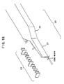
- Fig.18 is a magnified view of the spotsize converter provided in an input or output waveguide of an planar lightwave circuit
- Fig.19 shows a relationship between a taper angle and the excess loss
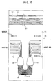
- Fig.20 shows an example of application of the spotsize converter according to this embodiment. Parts which are the same as those of the above-mentioned embodiments will not be described, and the same symbols as those used in the embodiments will be used.
- a spotsize converter 21 shown in Fig.18 is provided in the input/output waveguide in the planar lightwave circuit shown in Fig.4. Since the spotsize converters which are provided in the input waveguide and the output waveguide are the same, symbols are not provided in order to differentiate between the input waveguide and the output waveguide in the following figures.
- the spotsize converter 20 of the present invention includes a core width fine-tuning part 21 and a core width converting part 22 which follows the core width fine-tuning part 21.
- the difference between the parts 21 and 22 is the taper angle.
- the taper angle is defined as two times of ⁇ 1 or ⁇ 2 in Fig.18.
- the taper angle 2 ⁇ 1 of the core width fine-tuning part is set to be smaller than the taper angle 2 ⁇ 2 of the core width converting part 22.
- markers 23 which indicate dicing positions of a waveguide may be provided. Details of the markers will be described later.
- the input/output waveguide is formed as a taper shape such that optimum core width can be obtained with reliability by adjusting end face position.
- the taper angle 2 ⁇ 1 is set to be 0.057° in order to obtain ⁇ 0.1 ⁇ m accuracy of the core width in this embodiment.
- the waveguide and the optical fiber is connected and fixed by an adhesive. Since the refractive index of the adhesive is subtly different from that of the glass, light reflections occur on a connection surface. To prevent the reflected light from reentering the optical fiber or the optical waveguide, the end surfaces of an optical waveguide and an optical fiber are generally angle polished by 5° - 10° . In the current state that the input/output end face position is obtained by the angle polishing, it is difficult to obtain the input/output end face position with high accuracy. The accuracy of the end face position obtained by experiment was ⁇ 100 ⁇ m.
- the taper angle for fine-tuning part should be as small as possible to provide a higher degree of tolerance for angle polishing.
- the taper angle 2 ⁇ 1 is set to be 0.057° in order to obtain ⁇ 0.1 ⁇ m accuracy for finally obtained core width.
- taper length of 4.2mm is required when a simple taper is adopted where the core width is narrowed from 5 ⁇ m to 0.8 ⁇ m. Such a long taper is not desirable considering that the object of adopting the superhigh- waveguide is to downsize the planar lightwave circuit.
- the spotsize converter 21 is divided into two sections which are the core width converting part 22 in which the core width is decreased sharply to the extent that loss does not occur and the core width fine-tuning part 21 in which the taper angle is set to be small in consideration of error of the end face forming position.
- the taper angle 2 ⁇ 2 of the core width converting part is large to the extent that the excess loss does not occur. As shown in the relationship of the taper angle and the excess loss in Fig.19, it is evident that the smaller the taper angle is, the lower the excess loss is.
- 2 ⁇ 2 is set to be 1° so that the core width in the core width converting part is decreased from 5 ⁇ m to 1.5 ⁇ m. In this case, the length of the core width converting part becomes about 200 ⁇ m.
- the taper angle 2 ⁇ 1 is set to be 0.057° so that the core width decreases from 1.5 ⁇ m to 0.8 ⁇ m in order that accuracy for forming the optimum core width becomes ⁇ 0.1 ⁇ m.
- the length of the core width fine-tuning part is 700 ⁇ m.
- the sum of the lengths of the core width fine-tuning part and the core width converting part becomes 900 ⁇ m, which is about one-fifth of 4.2mm of the case when using the simple taper.
- the taper angle 2 ⁇ 2 of the core width converting part is larger than 0.08° and equal to or smaller than 10° . Because, when the taper angle 2 ⁇ 2 is equal to or smaller than 0.08° , the length of the core width converting part becomes too long so that downsizing can not be realized. When the taper angle 2 ⁇ 2 is larger than 10° , the excess loss becomes too large.
- the taper angle of the core width fine-tuning part is larger than 0° and equal to or smaller than 0.08° . Because, when the taper angle 2 ⁇ 1 is larger than 0.08° , the length of taper part becomes too short so that adequate accuracy is not obtained due to mechanical polishing error.
- the spotsize converter 20 shown in Fig.18 can be applied to the AWG which is described in the second embodiment as shown in Fig.20 in addition to the planar lightwave circuit shown in Fig.4.
- the spotsize converter of the present invention is provided in the input end side of the AWG 70 in which the core width decreases toward the input end, and the spotsize converter of the present invention is provided in the output end side of the AWG 70 in which the core width decreases toward the output end.
- the AWG can be formed such that the core widths of the end faces are different for each spotsize converter.
- the spotsize converters in the input end and the output end are formed such that the taper angles ⁇ 1 are different from each other, or, the positions of the spotsize converters are shifted to each other. Then, the substrate is cut straightly for obtaining a proper core width.
- dicing positions of the end faces can be determined by using the markers shown in Fig.18 and Fig.20. As shown in Fig.20, the markers may be provided only in the upper side of the spotsize converter or may be provided in the both sides of the spotsize converter.
- the above-mentioned waveguide can be fabricated in the same way as described in the above-mentioned embodiments.
- the waveguides can be made of polyimide, silicon, semiconductor, LiNbO 3 and the like in addition to silica-based glass.
- This embodiment can be also applied to the input/output ports which were described by Fig.16
- the arrayed waveguide grating AWG
- application of the present invention is not limited to the AWG since the point of the present invention is in the input/output waveguide including the spotsize converter so that the application of the present invention does not depend upon the kind of optical circuits.
- a spotsize converter 75 of the fifth embodiment of the present invention is shown in Fig.21, and magnified views of examples of the core width fine-tuning part 76 of Fig.21 are shown in Figs.22 and 23.
- the core width fine-tuning part 76 is formed by a simple tapered waveguide of the taper angle 2 ⁇ 1 in the fourth embodiment.
- the core width fine-tuning part is configured by taper and straight parts or a plurality of tapers in which taper angles may be different, instead of configured by the simple taper.
- the core width fine-tuning part may be formed by alternately connecting tapered waveguides 82 and straight waveguides 81.
- the core width fine-tuning part may be formed by steps of straight waveguides as shown in Fig.23.
- the coupling loss between the waveguide and an optical fiber decreases.
- the core width fine-tuning part when configured such that the mean taper angle 2 ⁇ 1 is 0.057° and the straight waveguide is repeated seven times where the length of a straight waveguide is 200 ⁇ m, the core width can be decreased from 1.5 ⁇ m to 0.8 ⁇ m.
- ⁇ 1 instead of 2 ⁇ 1 may be also called a mean taper angle.
- ⁇ 2 instead of 2 ⁇ 2 may be also called a mean taper angle.
- the above definition of the mean taper angle also can be used for the core width converting part.
- W2 in Fig.24 is used as the above-mentioned W1 in the equation (3)
- a core width of the waveguide other than the spotsize converter is used as the above-mentioned W2 in the equation (3)
- the length of the core width converting part is used as the above-mentioned L in the equation (3).
- the definition of the above-mentioned mean taper angle can be used for the spotsize converter of the first embodiment which does not have the core width converting part.
- a core width of the waveguide other than the spotsize converter part can be used as W2 in the equation (3) and the length of the spotsize converter can be used as L in the equation (3).
- the configurations shown in Fig.16 and Fig.20 can be realized.
- the present embodiment can be applied to various optical circuits in the same way as the fourth embodiment.
- monitor waveguides each of which has the spotsize converter of the present invention are provided separately from the planar lightwave circuit on a substrate on which the planar lightwave circuit is formed.
- Fig.25 shows an example in which the monitor waveguides and an AWG 90 like one shown in Fig.20 are provided on a substrate.
- Fig.26 shows the part of the monitor waveguides.
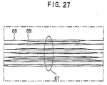
- seven monitor waveguides 87 are provided wherein locations of each spotsize converter which includes a core width fine-tuning part 88 and a core width converting part 89 are shifted to each other by 100 ⁇ m.
- the monitor waveguides By dicing these monitor waveguides collectively at a dicing position, the monitor waveguides have various core widths different from each other at the end face.
- Fig.27 shows the monitor waveguides after dicing.
- the planar lightwave circuits can be cut after the optimum core width is obtained by using the monitor waveguides.
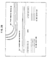
- Fig.28 shows a magnified view of a part including the monitor waveguides of this case.
- the right end sides of first monitor waveguides 92 in Fig.28 are straight.
- the planar lightwave circuit is cut.
- the coupling loss of the AWG can be estimated by using second monitor waveguides 93.
- the second monitor waveguides 93 may include a monitor waveguide having spotsize converters each of which is the same as that used in the input/output end of the AWG and a monitor waveguide which is straight in the both ends. In this case, difference of the excess loss between the two monitor waveguides represents the amount of the excess loss decreased by the spotsize converter.
- planar lightwave circuit which has the monitor waveguides and the planar lightwave circuit which is intended to be fabricated may be provided separately.
- markers shown in Fig.18 for example are provided such that the end face forming position in the core width fine-tuning part can be perceived when performing mechanical polishing process.
- the planar lightwave circuit can be configured, for example, such that when the coupling loss is lowest in the fifth monitor waveguide, the coupling loss can be minimized by processing the end face such that the position of the fifth marker becomes the end face.
- the markers can be provided in various forms. For example, markers shown in Figs. 29 - 32B can be provided.
- Fig.29 shows a first example of the markers in which vertical lines 95 are placed at regular intervals like a ruler. As shown in Fig.29, symbols (numerals) may be provided. The cutting position can be determined by reading the markers.
- Figs.30A - 30C show a second example of the markers, which indicate positions where the shape of the spotsize converter changes.
- the optimum core width can be obtained by cutting a part between two markers, for example.
- Figs.31A - 31B show a third example of the markers where the width of a marker 96 of the upper side is the same as cutting width and a marker 97 of the lower side indicate an end face position after cutting. Accordingly, cutting can be performed in consideration of cutting width.
- Figs.32A and 32B show a fourth example of the markers.
- the fourth example is almost the same as the third example shown in Figs. 31A and 31B.
- the difference is that the markers are placed in consideration of the amount which is trimmed due to mechanical polishing.
- a curve shape such as an exponential and a parabola can be used as the taper part in addition to the shape where the core width changes linearly.
- an optimized taper which is proposed in "Soon Ryong Park and Beom-hoan O, "Novel Design Concept of Waveguide Mode Adapter for Low-Loss Mode Conversion", IEEE PHOTONICS TECHNOLOGY LETTERS, VOL.13, NO.7, JULY 2001, pp.675-677" can be used as the taper shape of the core width converting part shown in Fig.18 for example. Accordingly, the coupling loss can be further decreased.
- the optimized taper can be also used for the core width fine-tuning part.
- the spotsize converter of the present invention is not limited to the planar lightwave circuit.
- the spotsize converter can be applied to any optical circuit such as an optical circuit in which optical circuits or waveguides are multilayered.
- the "optical circuit" in this specification is used for meaning general optical circuit which is not limited to the planar lightwave circuit or the waveguide type optical circuit like AWG.
- the main object of the present invention is to decrease the coupling loss between an optical waveguide and an optical fiber
- the coupling loss also can be decreased when an optical component which is formed by a waveguide type optical circuit such as semiconductor laser is connected to the optical fiber or the planar lightwave circuit by using the optimum core width.
- the present invention can be used when different optical circuits are connected with each other.
- the coupling loss of the superhigh- waveguide can be decreased while downsizing the planar lightwave circuit.
- dicing error which may occur when dicing the substrate can be dissolved.
- low coupling loss can always be obtained by selecting and using a port which has the optimum core width. Therefore, the planar lightwave circuits, especially, low loss and highly integrated planar lightwave circuits can be applied to an optical communication system efficiently. Thus, a large capacity optical communication system which is in increasing demand can be constructed.
Landscapes
- Physics & Mathematics (AREA)
- Engineering & Computer Science (AREA)
- Microelectronics & Electronic Packaging (AREA)
- General Physics & Mathematics (AREA)
- Optics & Photonics (AREA)
- Power Engineering (AREA)
- Optical Integrated Circuits (AREA)
Abstract
Description
- The present invention relates to a planar lightwave circuit (PLC) which can decrease the coupling loss between a planar lightwave circuit and an optical fiber or between planar lightwave circuits.
- It is predicted that the planar lightwave circuits will be used more and more as main parts which have important functions such as routing of an optical signal in superfast large-capacity optical communication systems from now on. Especially, it is required to construct a larger optical communication system as capacity required for communication increases. In order to realize the enlargement of the optical communication system, it is necessary to downsize the planar lightwave circuit and to allow connection between many planar lightwave circuits.
- Fig.1 is a schematic diagram of structure of a conventional planar lightwave circuit. As shown in Fig.1, an
input waveguide 112 is formed on asubstrate 111. Theinput waveguide 112 is connected to aslab waveguide 113 formed on thesubstrate 111. One end of a plurality ofarrayed waveguides 114 formed on thesubstrate 111 is connected to theslab waveguide 113. Ahalf waveplate 115 which gets rid of polarization dependence is provided at some midpoint of thearrayed waveguides 114. The other end of thearrayed waveguides 114 is connected to aslab waveguide 116 formed on thesubstrate 111. A plurality of output waveguides formed on thesubstrate 111 are connected to theslab waveguide 116. - When an optical signal is entered into the
planar lightwave circuit 110 from theinput waveguide 112, the optical signal is entered into thearrayed waveguides 114 via theslab waveguide 113 and polarization dependence is dissolved by thehalf waveplate 115. In addition, the optical signal is demultiplexed into signals of various wavelengths in theslab waveguide 116 due to delay line of thearrayed waveguides 114 so that demultiplexed signals are output from theoutput waveguides 117. - In order to downsize the
planar lightwave circuit 110, it is very effective to adopt a waveguide (which will be called a superhigh-waveguide) in which relative refractive index difference is a high value which is larger than 1%, where relative refractive index difference
 is the ratio of difference between the refractive index ncore of the core and refractive index nclad of the cladding to the refractive index ncore of the core as represented by the following equation (1). The reason is that the higher the relative refractive index difference
 is, the more completely the light is confined in the waveguide so that the waveguide can be used even when it is bent by a small bending radius.

- However, there is a problem in that the coupling loss of the superhigh-waveguide is very large.

- As shown in Fig.2, when an optical signal which propagates through a
core 120a in anoptical fiber 120 enters into acore 112a of theinput waveguide 112, attenuation of the optical signal, which is called the coupling loss, occurs. The coupling loss occurs when connecting different types of waveguides. The coupling loss occurs due to difference of field distribution between the different types of waveguides, and the coupling loss accumulates as connecting points increases. For example, as for 1.5µm wavelength which is used in an optical communication system, large coupling loss about 3.5dB occurs between a single-mode optical fiber of core diameter 9µm and a superhigh-waveguide about 5µm per side.
- In the
planar lightwave circuit 110 used in the optical communication system, downsizing and decreasing of the coupling loss are mutually contradictory. That is, although the circuit can be downsized by increasing - As a method for decreasing the coupling loss between the superhigh-waveguide and the optical fiber, use of a spotsize converter in which core width is narrowed toward an end face of a substrate is known as shown in Fig.3 (for example, Japanese laid-open patent application No.63-280202).

- There is an region in which a spotsize is widened when the core width is narrowed to some extent. Then, it becomes possible to decrease the coupling loss by adjusting the widened field distribution with that of an optical fiber.
- However, it is known that the coupling loss for the narrow taper spotsize converter largely changes due to slight fabrication error of core width,and the like. Thus, the narrow taper spotsize converter has not been in practical use.

- It is an object of the present invention to provide a planar lightwave circuit which can suppress the coupling loss while downsizing is realized.
- More particularly, it is an object of the present invention to provide a planar lightwave circuit and an optical circuit which use a narrow taper spotsize converter which has large fabrication tolerance.
- The above object of the present invention is achieved by a planar lightwave circuit in which an input waveguide and an output waveguide are formed on a substrate wherein each of the input waveguide and the output waveguide are formed by a core and a cladding which covers the core, and refractive index of the core is higher than refractive index of the cladding, wherein:
- a core width of each of an input end side of the input waveguide and an output end side of the output waveguide changes gradually toward an end face of the substrate.
-
- In the planar lightwave circuit, a taper part is formed in the core in each of the input end side of the input waveguide and the output end side of the output waveguide, and a taper angle of the taper part is larger than 0° and equal to or smaller than 5° .
- In the planar lightwave circuit, steps are formed in the core in each of the input end side of the input waveguide and the output end side of the output waveguide.
- In the planar lightwave circuit, height between adjacent steps in the steps is larger than 0 µm and equal to or smaller than 5µm.
- In the planar lightwave circuit, taper parts and straight parts are formed alternately in the core in each of the input end side of the input waveguide and the output end side of the output waveguide, core width of each of the taper parts changes gradually toward an end face of the substrate and core width of each of the straight parts is constant.
- In the planar lightwave circuit, length of each of the straight parts is equal to or larger than 1µm.
- In the planar lightwave circuit, a marker is provided for indicating a cutting position of the input waveguide or the output waveguide, or indicating a position where the core width changes.
- The planar lightwave circuit may include a monitor waveguide in which an input end of the monitor waveguide is formed in an end face side of the substrate which is different from end face sides in which the input end of the input waveguide and the output end of the output waveguide are provided, wherein the monitor waveguide includes a core which is formed such that core width changes toward an end face of the substrate.
- In addition, the planar lightwave circuit may include a monitor waveguide, wherein an input end of the monitor waveguide is formed in an end face side of the substrate in which the input end of the input waveguide is located, and
- an output end of the monitor waveguide is formed in an end face side of the substrate in which the output end of the output waveguide is located, wherein shapes of an input end side and an output end side of the monitor waveguide are similar to the input end side of the input waveguide and the output end side of the output waveguide respectively.
-
- In the planar lightwave circuit, the substrate is made of silicon and the input waveguide and the output waveguide are made of silica-based glass.
- The object of the present invention is also achieved by an optical circuit which includes a waveguide and a spotsize converter which is a part of the waveguide, wherein a core is embedded in a cladding in the waveguide, and the spotsize converter is located near an end face of a substrate on which the optical circuit is formed, the spotsize converter including:
- alternating taper parts and straight parts;
- wherein core width of each of the taper parts decreases toward an end face of the substrate and core width of each of the straight parts is constant.
-
- In the optical circuit, an optimized taper is used as a shape of the taper part.
- In addition, the object of the present invention is achieved by an optical circuit which includes a waveguide and a spotsize converter which is a part of the waveguide, wherein a core is embedded in a cladding in the waveguide, and the spotsize converter is located near an end face of a substrate on which the optical circuit is formed, the spotsize converter including:
- a plurality of straight parts via steps, core width of each straight part being constant;
- wherein core width of the spotsize converter is minimum at an end face of the substrate, and a height of the step is larger than 0µm and equal to or smaller than 5µm.
-
- In the optical circuit, a length of the straight part is equal to or larger than 1µm.
- In the optical circuit, a mean taper angle of the spotsize converter is larger than 0° and equal to or smaller than 5°.
- The object of the present invention is also achieved by an optical circuit which includes a waveguide and a spotsize converter which is a part of the waveguide, wherein a core is embedded in a cladding in the waveguide, and the spotsize converter is located near an end face of a substrate on which the optical circuit is formed, the spotsize converter including:
- a core width fine-tuning part in an end face side of the substrate; and
- a core width converting part which follows the core width fine-tuning part;
- wherein core width of said spotsize converter is minimum at an end face of said substrate, a mean taper angle 1 of the core width fine-tuning part is larger than 0° and smaller than a mean taper angle 2 of the core width converting part.
-
- In the optical circuit, the core width fine-tuning part may include a plurality of taper parts.
- In the optical circuit, the core width fine-tuning part may include alternating taper parts and straight parts, core width of each straight part being constant.
- In the optical circuit, the core width fine-tuning part may include;
- a plurality of straight parts via steps, core width of each straight part being constant;
- wherein a height of the step is larger than 0µm and equal to or smaller than 5µm.
-
- In the optical circuit, an optimized taper is used as a shape of the core width converting part.
- In the optical circuit, a mean taper angle 1 of the core width fine-tuning part is larger than 0° and equal to or smaller than 0.04° ,and a mean taper angle 2 of the core width converting part is larger than 0.04° and equal to or smaller than 5° .
- In the optical circuit, a marker for forming an end face of the substrate is provided in the optical circuit.
- In the optical circuit, the marker is provided in a location corresponding to a location in which a shape of the core width fine-tuning part changes.
- In the optical circuit, a monitor waveguide is provided on the substrate, the monitor waveguide including a second spotsize converter including:
- a second core width fine-tuning part in an end face side of the substrate; and
- a second core width converting part which follows the second core width fine-tuning part;
- wherein core width of said second spotsize converter is minimum at an end face of said substrate, a mean taper angle 1 of the second core width fine-tuning part is larger than 0° and smaller than a mean taper angle 2 of the second core width converting part.
-
- The optical circuit includes a plurality of the monitor waveguides, spotsize converters of the monitor waveguides are shifted to each other by a predetermined distance in the direction of the length of the monitor waveguides.
- In addition, the optical circuit may include a first monitor waveguide and a second monitor waveguide;
- wherein the first monitor waveguide includes a first spotsize converter in an end face side of the substrate which is different from end face sides corresponding to an input end or an output end of the waveguide, the first spotsize converter including:
- a first core width fine-tuning part in an end face side of the substrate;
- a first core width converting part which follows the first core width fine-tuning part;
- wherein core width of said first spotsize converter is minimum at an end face of said substrate, a mean taper angle 1 of the first core width fine-tuning part is larger than 0° and smaller than a mean taper angle 2 of the first core width converting part;
- wherein the second monitor waveguide includes a second spotsize converter in an end face side of the substrate where an input end or an output end of the waveguide is located, the second spotsize converter including:
- a second core width fine-tuning part in an end face side of the substrate;
- a second core width converting part which follows the second core width fine-tuning part;
- wherein core width of said second spotsize converter is minimum at an end face of said substrate, a mean taper angle 1 of the second core width fine-tuning part is larger than 0° and smaller than a mean taper angle 2 of the second core width converting part
-
- In addition, the object of the present invention is also achieved by an optical circuit which includes input ports and output ports, each of the input ports and the output ports including:
- a waveguide and a spotsize converter which
is a part of the waveguide, wherein a core is
embedded in a cladding in the waveguide, and the
spotsize converter is located near an end face of a
substrate on which the waveguide is formed, the
spotsize converter including:
- a core width fine-tuning part in an end face side of the substrate; and
- a core width converting part which follows the core width fine-tuning part;
- wherein a mean taper angle 1 of the core width fine-tuning part is larger than 0° and smaller than a mean taper angle 2 of the core width converting part.
-
- Other objects, features and advantages of the present invention will become more apparent from the following detailed description when read in conjunction with the accompanying drawings, in which:
- Fig.1 is a schematic diagram of structure of a conventional planar lightwave circuit;
- Fig.2 is a figure for explaining the connection between an input waveguide of a conventional planar lightwave circuit and an optical fiber;
- Fig.3 is an example of a spotsize converter according to a conventional technique;
- Fig.4 is a schematic block diagram of a planar lightwave circuit of a first example of a first embodiment of the present invention;
- Fig.5 is a magnified view of the core of the input waveguide and the output waveguide of the planar lightwave circuit of Fig.4;
- Figs.6A - 6E are diagrams for explaining a process for fabricating the input waveguide and the output waveguide of the planar lightwave circuit of Fig.4;
- Fig.7 shows a relationship between the core width and the coupling loss of the end face of the substrate which is obtained by calculation;
- Fig.8 is a diagram for explaining dicing error;
- Fig.9 is a magnified view of the core of the input waveguide and the output waveguide of the planar lightwave circuit of a second example of a first embodiment of the present invention;
- Fig.10 is a magnified view of the core of the input waveguide and the output waveguide of the planar lightwave circuit of a third example of a first embodiment of the present invention;
- Figs.11A and 11B are magnified views of surrounding areas of the core of the input waveguide and the output waveguide of the planar lightwave circuit of a fourth example of a first embodiment of the present invention;
- Fig.12 shows a schematic block diagram of the planar lightwave circuit of a first example of a second embodiment of the present invention;
- Fig.13 shows a magnified view of the core of the input waveguides or the output waveguides of the planar lightwave circuit shown in Fig.12;
- Fig.14 is a figure for explaining a fabricating method of the core shown in Fig.13;
- Fig.15 is a figure for explaining another fabricating method of the core shown in Fig.13;
- Fig.16 shows a schematic block diagram of the planar lightwave circuit of a second example of the second embodiment of the present invention;
- Fig.17 shows a schematic block diagram of the planar lightwave circuit of a third embodiment of the present invention;
- Fig.18 is a magnified view of the spotsize converter provided in an input or output waveguide of the planar lightwave circuit of a fourth embodiment of the present invention;
- Fig.19 shows a relationship between a taper angle and the excess loss which is obtained by calculation;
- Fig.20 shows an example of application of the spotsize converter according to the fourth embodiment;
- Fig.21 is a magnified view of the spotsize converter provided in an input or output waveguide of the planar lightwave circuit of a fifth embodiment of the present invention;
- Fig.22 shows an example of a core width fine-tuning part of the fifth embodiment;
- Fig.23 shows another example of a core width fine-tuning part of the fifth embodiment;
- Fig.24 is a figure for explaining a definition of a mean taper angle;
- Fig.25 shows a schematic block diagram of the planar lightwave circuit of a sixth embodiment of the present invention;
- Fig.26 shows monitor waveguides in the sixth embodiment;
- Fig.27 shows the monitor waveguides after dicing;
- Fig,28 shows another example of monitor waveguides in the sixth embodiment;
- Fig.29 shows a first example of markers of the planar lightwave circuit of the present invention;
- Figs.30A - 30C show second examples of markers of the planar lightwave circuit of the present invention;
- Figs.31A - 31B show third examples of markers of the planar lightwave circuit of the present invention;
- Figs.32A - 32B show fourth examples of markers of the planar lightwave circuit of the present invention.
-
- As described in the related art, as for the spotsize converter which uses the narrow taper, fabrication tolerance of core width is very narrow for minimizing the coupling loss between the planar lightwave circuit and the optical fiber. That is, an optimum value of the core width changes due to fabrication conditions of the relative refractive index differencebetween the core and the cladding, core thickness and the like. According to the present invention, the core width of the input waveguide is narrowed toward the end face of the substrate to allow the core width to be fine-tuned so that the optimum core width can be obtained. By adjusting the position of the end face, the optimum core width can be obtained with high reproducibility,

- In the following, although each embodiment of the present invention will be described, the present invention is not limited to the embodiments.
- The first example of the first embodiment of the planar lightwave circuit of the present invention will be described with reference to Figs.4 - 8. Fig.4 is a schematic block diagram of the planar lightwave circuit, Fig.5 is a magnified view of the core of the input waveguide and the output waveguide of the planar lightwave circuit of Fig.4. Figs.6A - 6E are diagrams for explaining a process for fabricating the input waveguide and the output waveguide of the planar lightwave circuit of Fig.4. Fig.7 shows a relationship between the core width and the coupling loss of the end face of the substrate which is obtained by calculation. Fig.8 is a diagram for explaining dicing error.
- As shown in Fig.4, an
input waveguide 12 made of silica-based glass is formed on asubstrate 11 made of silicon in which theinput waveguide 12 includes a core having high refractive index and a cladding having low refractive index, and the core is covered by the cladding. As shown in Fig.5, thecore 12a of theinput waveguide 12 has a taper part 12aa in which the core width decreases gradually toward the input end which is located in the end face side of thesubstrate 11. - In each embodiment, the part of the waveguide in which the core width decreases gradually from a part near the end face of the substrate toward the end face of the substrate will be called a spotsize converter. For example, the taper part shown in Fig.5 is a spotsize converter.
- As shown in Fig.4, the
input waveguide 12 is connected to aslab waveguide 13 made of silica-based glass. Each one end of arrayedwaveguide 14 made of silica-based glass formed on thesubstrate 11 is connected to theslab waveguide 13. Ahalf waveplate 15 for dissolving polarization dependence is provided at some midpoint of the arrayedwaveguides 14. The other ends of the arrayedwaveguides 14 are connected to aslab waveguide 16 made of silica-based glass formed on thesubstrate 11. -
Output waveguides 17 made of silica-based glass formed on thesubstrate 11 are connected to theslab waveguide 16. In the same way as theinput wave guide 12, thecore 17a of theoutput waveguide 17 has a taper part 17aa in which the core width decreases gradually toward the output end which is located in another end face side of thesubstrate 11 as shown in Fig.5. - The
waveguide - First, undercladding glass soot mainly made of SiO2 is deposited on the
substrate 11 made of silicon by a flame hydrolysis deposition (FHD) method. Then, core glass soot in which GeO2 is doped to SiO2 is deposited on the undercladding glass soot by the flame hydrolysis deposition method. After that, high temperature heat-treatment (larger than 1000°C) is carried out for the glass soot such that the glass soot becomes transparent. Accordingly, an undercladding glass 12ba and acore glass 12a are formed on the substrate 11 (Fig.6A). Thickness is adjusted such that thickness of the undercladding glass 12ba and thecore glass 12a become proper when depositing the glass soot by the flame hydrolysis deposition method. - Next, etching
masks 100 are formed on thecore glass 12a using photolithography such that eachetching mask 100 becomes tapered structure, that is, width of eachetching mask 100 decreases toward the end face of the substrate 11 (Fig.6B). After that, patterning of thecore glass 12a is performed (Fig.6C), and the etching masks 100 are removed (Fig.6D). - Finally, overcladding glass 12bb mainly made of SiO2 is deposited on the undercladding glass 12ba and the
core glass 12a by the flame hydrolysis deposition method so that the overcladding glass 12bb also spreads into a narrow spacing between the adjacent core glasses, wherein dopant such as B2O3 and P2O5 is doped in the overcladding glass 12ba so that glass transition temperature is lowered (Fig.6E). Then, thewaveguide substrate 11. - In the
planar lightwave circuit 10, when an optical signal in which lights of a plurality of different wavelengths are multiplexed is entered in theinput waveguide 12, the optical signal is entered in the arrayedwaveguides 14 via theslab waveguide 13, and polarization dependence is dissolved by thehalf waveplate 15. In addition, the optical signal is demultiplexed into optical signals of the wavelengths in theslab waveguide 16 due to delay line of the arrayedwaveguides 14. Then, the optical signals are output from theoutput waveguides 17. - Fig.7 shows a relationship between the core width at the end face of the substrate and the coupling loss which is calculated for a single-mode optical fiber of 9µm core diameter, in which the core thickness is 5µm andis 1.5%. As is known from this figure, as the core width is decreased gradually from 5µm, the spotsize in the waveguide decreases so that the coupling loss increases. However, when the core width becomes smaller than 4 µm, confinement of light into the core becomes weak and the spotsize is widened so that the coupling loss becomes lowered. When the core width is further decreased, the coupling loss becomes minimum at core width close to 1.2µm. However, the coupling loss increases rapidly as the core width decreases below 1.2µm. This is because the spotsize rapidly increases since the core width is too narrow.

- As shown in Fig. 7, when the core width is 1.2µm, the coupling loss reaches its minimum value of approximately 0.5dB. Thus, the coupling loss can be suppressed to about 1.0dB in total of both ends of input and output. Since the waveguide is designed such that a single-mode light propagates, width and thickness of the core of the waveguide are determined by the material and the like.
- Thus, the taper part 12aa, 17aa is provided in the
core waveguide substrate 11 in theplanar lightwave circuit 10 of the first example in this embodiment. Accordingly, the coupling loss is decreased while satisfying propagation conditions of the single-mode light. - As mentioned above, the coupling loss increases rapidly when the core width deviates from 1.2µm even slightly. Thus, there is a possibility in that the coupling loss may increase due to deviation from optimum width caused by dicing error of the
planar lightwave circuit 10. - As shown in Fig.8, when assuming that a taper angle of the taper part 12aa, 17aa is , and amount of deviation of dicing position is

- For example, when is 1.5° and
- Therefore, if error occurs when dicing the
planar lightwave circuit 10, the error does not largely affect the coupling loss so that theplanar lightwave circuit 10 of low coupling loss can be always fabricated easily. - It is desirable that the taper angle of the taper part 12aa, 17aa of the
core waveguide - In the above-mentioned
planar lightwave circuit 10, silica-basedwaveguides 11∼17 are formed on thesilicon substrate 11. However, materials are not limited to these. Thewaveguides 11∼17 which are made of polyimide, silicon, semiconductor, LiNbO3 and the like can be formed on thesubstrate 11 which is made of various materials. - Instead of providing a simple taper shown in Fig.5, a
core core substrate 11. - If the number of the steps are increased so as to decrease the height difference
core - That is, when low coupling loss can not be obtained at a dicing position, the waveguide can be used after cutting the substrate at a different position, since the core width becomes smaller toward the input end or the output end by using the steps 32aa, 37aa. Therefore, even when an accurate optimum core width is not known and only an estimated value of an analytic result is obtained, the optimum core width can be searched for by changing the cutting position.
- Therefore, by applying the
core - It is desirable that the height difference between the adjacent steps
- In the example shown in Fig.9, the height
- In addition, as shown in Fig.10, a
core core substrate 11, wherein the core width becomes smaller toward the input or output end as for the taper part, and the core width is fixed at a constant width as for the straight part which is formed along the axis of the core. - By applying the
core - It is desirable that the length s of the straight part 42ab, 47ab is equal to or larger than 1µm. Because, when s is smaller than 1µm, it becomes difficult to absorb dicing error.
- As for the example shown in Fig.10, although the lengths of the taper parts and the straight part are fixed, it is possible to form the core such that the lengths are different.
- For example, as shown in Figs.11A and 11B, markers La1, La2 which indicate dicing positions may be formed near the input or output end of 'the waveguide of the
planar lightwave circuit 10 when fabricating theplanar lightwave circuit 10. In addition, markers Lb1, Lb2 which indicate changing positions of core width may be provided, By providing these markers, the accuracy of dicing can be easily improved. - A first example of the second embodiment will be described with reference to Figs.12 and 13. Fig.12 shows a schematic block diagram of the planar lightwave circuit, Fig.13 shows a magnified view of the core of the input waveguides or the output waveguides. Parts which are the same as those of the first embodiment are not described, and the same symbols as those used in the first embodiment are used.
- In this embodiment, the present invention is applied to an arrayed waveguide grating (AWG), which is one of planar lightwave circuits, which performs multiplexing of optical signals of a plurality of different wavelengths and demultiplexing in an wavelength division multiplexing communication system. AWG is an example of a waveguide type optical circuit.
- As shown in Fig.12, a plurality of
input waveguides 12 are provided on thesubstrate 11. The core width of input end face of the taper part 12aa of thecore 12a is different by each input waveguide as shown in Fig.13. - In addition, a plurality of
output waveguides 17 are provided on thesubstrate 11. The core width of input end face of the taper part 17aa of thecore 17a is different by each output waveguide as shown in Fig.13. - The
waveguide AWG 50 can be fabricated in the same way as theplanar lightwave circuit 10 in the first embodiment basically. For example, as shown in Fig.14, etching masks of taper shape are formed, wherein the width of each etching mask becomes smaller toward the end of the substrate, and the taper angle of the etching masks is different from each other. Or, as shown in Fig.15, etching masks which have the same taper angle may be provided in which the position of the spotsize converters are shifted in the horizontal direction. Then, reactive ion etching is performed and the substrate is cut straightly. Accordingly, thecores - In the
AWG 50 which has such structure, when an optical signal in which lights of a plurality of different wavelengths are multiplexed is entered in any one ofinput waveguides 12, the optical signal is entered in the arrayedwaveguides 14 via theslab waveguide 13, and polarization dependence is dissolved by thehalf waveplate 15. In addition, the optical signal is demultiplexed into optical signals of the wavelengths in theslab waveguide 16 due to delay line of the arrayedwaveguides 14. Then, the optical signals are output from theoutput waveguides 17. - According to the
AWG 50, since the core width of thetaper part - The multiplexed optical signal entered from an input port (which is not shown in the figure) which is connected to the
input waveguide 12 is demultiplexed into signals having different wavelengths and the demultiplexed signals are output from output ports (which is not shown in the figure) connected to theoutput waveguides 17. The coupling loss varies from output port to output port since the core width varies from output port to output port due to dicing error. - Thus, a plurality of
input waveguides 12 in which the core width is different from each other are provided and an input port is connected to each input waveguides 12. As a result, an input port to decrease the coupling loss can be selected for each output port. In addition, since the sum of the coupling losses of an input port and an output port can be selected to be constant, value of the coupling loss can be rendered equal for each port. - It is also possible to apply the
core - In addition, it is also possible to apply the
core substrate 11, wherein the core width becomes smaller toward the input or output end as for the taper part, and the core width is fixed at a constant width as for the straight part which is formed along the axis of the core. - In the first example of this embodiment, an input port is selected among input ports connected to the
input waveguides 12 such that the coupling loss becomes smallest. In addition, when it is necessary to use every input waveguide 12, a configuration shown in Fig.16 can be adopted. The optical circuit shown in Fig.16 includesAWG 50, input ports i and output ports j. The input port i includes a plurality of input waveguides which were described in the first embodiment and each input port is connected to aninput waveguide 12 ofAWG 50. The output port j includes a plurality of the output waveguides which were described in the first embodiment and each output waveguide is connected to anoutput waveguide 17 of theAWG 50. In each input port i, an input waveguide is selected so that signal light is input to aninput waveguide 12 ofAWG 50, and the signal light is output from output waveguides of the output port j connected to anoutput waveguide 17 of theAWG 50. Therefore, the coupling loss can be decreased in every port i, j regardless of fabrication error. - The third embodiment of the planar lightwave circuit of the present invention will be described with reference to Fig.17. Fig.17 is a schematic block diagram of the planar lightwave circuit. Parts which are the same as those of the first and second embodiments will not be described, and the same symbols as those used in the first and second embodiments will be used.
- As shown in Fig.17,
first monitor waveguides 68 andsecond monitor waveguides 69 are provided on thesubstrate 11. As for thefirst monitor waveguides 68, input ends 68a are located in an end face side of thesubstrate 11 other than end face sides where the input ends and output ends of theinput waveguides 12 andoutput waveguides 17 are located. In addition, the input end side of the first monitor waveguide is formed as taper such that the core width is decreased toward the input end. The core widths of the input ends 68a are different from each other. Further, the output ends 68b are located in the end face side of thesubstrate 11 where the output ends of theoutput waveguides 17 are located. - As for the
second monitor waveguides 69, structures of the input ends 69a and the output ends 69b are the same as those of theinput waveguides 12 and theoutput waveguides 17 respectively. That is, the input ends 69a are located in an end face side of thesubstrate 11 where the input ends of theinput waveguides 12 are located. In addition, each of theinput end sides 69a are formed as taper such that the core width becomes smaller toward the input end, and, the core widths of the input ends 69a are different from each other. The output ends 69b are located in an end face side of thesubstrate 11 where the output ends of theoutput waveguides 17 are located. In addition, each of the output end sides 69b are formed as taper such that the core width becomes smaller toward the output end, and, the core widths of the output ends 69b are different from each other. - According to the
AWG 60 on which themonitor waveguides input waveguides 12 and the core widths of the output end face of theoutput waveguides 17 can be set as proper sizes in the following way. - The input ends 68a of the
monitor waveguides 68 on thesubstrate 11 are cut and the coupling loss of eachmonitor waveguide 68 is measured repeatedly so that the dependence of the coupling loss on the core width is checked. As a result, an optimum core width is obtained. After that, the end sides of theinput waveguides 12 and theoutput waveguides 17 are cut such that the optimum core width is realized. - In addition, by measuring the coupling losses of the
monitor waveguides 69, dicing error of theinput waveguides 12 and theoutput waveguides 17 can be checked. - According to the
AWG 60 of this embodiment, dicing error which occurs for eachindividual substrate 11 can be monitored, and optimum core width can be formed for theindividual substrate 11. - Although examples in which the spotsize converter is applied to the AWG have been described in the above-mentioned second and third embodiments, it is not limited to the AWG. The present invention can be applied to any planar lightwave circuit and to any optical circuit by providing input and output waveguides where the core widths are different and selecting an optimum port when using the planar lightwave circuit. As a result, the coupling loss can be decreased irrespective of fabrication error,
- Next, the fourth embodiment of the present invention will be described with reference to Figs.18 - 20.
- Fig.18 is a magnified view of the spotsize converter provided in an input or output waveguide of an planar lightwave circuit, Fig.19 shows a relationship between a taper angle and the excess loss. Fig.20 shows an example of application of the spotsize converter according to this embodiment. Parts which are the same as those of the above-mentioned embodiments will not be described, and the same symbols as those used in the embodiments will be used.
- In this embodiment, a
spotsize converter 21 shown in Fig.18 is provided in the input/output waveguide in the planar lightwave circuit shown in Fig.4. Since the spotsize converters which are provided in the input waveguide and the output waveguide are the same, symbols are not provided in order to differentiate between the input waveguide and the output waveguide in the following figures. - As shown in Fig.18, the
spotsize converter 20 of the present invention includes a core width fine-tuningpart 21 and a corewidth converting part 22 which follows the core width fine-tuningpart 21. The difference between theparts taper angle 21 of the core width fine-tuning part is set to be smaller than thetaper angle 22 of the corewidth converting part 22. In addition,markers 23 which indicate dicing positions of a waveguide may be provided. Details of the markers will be described later. - In the following, design parameters of the core width fine-tuning
part 21 and the corewidth converting part 22 will be described in detail. - As mentioned so far, according to the present invention, the input/output waveguide is formed as a taper shape such that optimum core width can be obtained with reliability by adjusting end face position. However, since the end face position of the waveguide is realized with accuracy of only about ±100µm, the
taper angle 21 is set to be 0.057° in order to obtain ±0.1µm accuracy of the core width in this embodiment. - Generally, the waveguide and the optical fiber is connected and fixed by an adhesive. Since the refractive index of the adhesive is subtly different from that of the glass, light reflections occur on a connection surface. To prevent the reflected light from reentering the optical fiber or the optical waveguide, the end surfaces of an optical waveguide and an optical fiber are generally angle polished by 5° - 10° . In the current state that the input/output end face position is obtained by the angle polishing, it is difficult to obtain the input/output end face position with high accuracy. The accuracy of the end face position obtained by experiment was ±100µm.
- Therefore, the taper angle for fine-tuning part should be as small as possible to provide a higher degree of tolerance for angle polishing. Thus, as mentioned above, according to this embodiment, the
taper angle 21 is set to be 0.057° in order to obtain ±0.1µm accuracy for finally obtained core width. - In this case, taper length of 4.2mm is required when a simple taper is adopted where the core width is narrowed from 5µm to 0.8µm. Such a long taper is not desirable considering that the object of adopting the superhigh-
- Therefore, according to the present invention, the
spotsize converter 21 is divided into two sections which are the corewidth converting part 22 in which the core width is decreased sharply to the extent that loss does not occur and the core width fine-tuningpart 21 in which the taper angle is set to be small in consideration of error of the end face forming position. - It is desirable that the
taper angle 22 of the core width converting part is large to the extent that the excess loss does not occur. As shown in the relationship of the taper angle and the excess loss in Fig.19, it is evident that the smaller the taper angle is, the lower the excess loss is. In this embodiment, 22 is set to be 1° so that the core width in the core width converting part is decreased from 5µm to 1.5µm. In this case, the length of the core width converting part becomes about 200µm. - As for the core width fine-tuning part, as mentioned above, the
taper angle 21 is set to be 0.057° so that the core width decreases from 1.5µm to 0.8µm in order that accuracy for forming the optimum core width becomes ±0.1µm. In this case, the length of the core width fine-tuning part is 700 µm. - As a result, the sum of the lengths of the core width fine-tuning part and the core width converting part becomes 900µm, which is about one-fifth of 4.2mm of the case when using the simple taper.
- It is desirable that the
taper angle 22 of the core width converting part is larger than 0.08° and equal to or smaller than 10° . Because, when thetaper angle 22 is equal to or smaller than 0.08° , the length of the core width converting part becomes too long so that downsizing can not be realized. When thetaper angle 22 is larger than 10° , the excess loss becomes too large. - In addition, the taper angle of the core width fine-tuning part is larger than 0° and equal to or smaller than 0.08° . Because, when the
taper angle 21 is larger than 0.08° , the length of taper part becomes too short so that adequate accuracy is not obtained due to mechanical polishing error. - The
spotsize converter 20 shown in Fig.18 can be applied to the AWG which is described in the second embodiment as shown in Fig.20 in addition to the planar lightwave circuit shown in Fig.4. - In this case, the spotsize converter of the present invention is provided in the input end side of the
AWG 70 in which the core width decreases toward the input end, and the spotsize converter of the present invention is provided in the output end side of theAWG 70 in which the core width decreases toward the output end. - In addition, in the same way as the second embodiment, the AWG can be formed such that the core widths of the end faces are different for each spotsize converter. In order to form the AWG like this, the spotsize converters in the input end and the output end are formed such that the taper angles 1 are different from each other, or, the positions of the spotsize converters are shifted to each other. Then, the substrate is cut straightly for obtaining a proper core width.
- In addition, dicing positions of the end faces can be determined by using the markers shown in Fig.18 and Fig.20. As shown in Fig.20, the markers may be provided only in the upper side of the spotsize converter or may be provided in the both sides of the spotsize converter.
- The above-mentioned waveguide can be fabricated in the same way as described in the above-mentioned embodiments. The waveguides can be made of polyimide, silicon, semiconductor, LiNbO3 and the like in addition to silica-based glass.
- This embodiment can be also applied to the input/output ports which were described by Fig.16 In addition, although the arrayed waveguide grating (AWG) has been adopted as an example of the planar lightwave circuit in this embodiment, application of the present invention is not limited to the AWG since the point of the present invention is in the input/output waveguide including the spotsize converter so that the application of the present invention does not depend upon the kind of optical circuits.
- A
spotsize converter 75 of the fifth embodiment of the present invention is shown in Fig.21, and magnified views of examples of the core width fine-tuningpart 76 of Fig.21 are shown in Figs.22 and 23. - This embodiment is almost the same as the fourth embodiment where a difference is in the core width fine-tuning
part 76. As shown in Fig.18, the core width fine-tuning part is formed by a simple tapered waveguide of thetaper angle 21 in the fourth embodiment. On the other hand, in this embodiment, as shown in Fig.21, the core width fine-tuning part is configured by taper and straight parts or a plurality of tapers in which taper angles may be different, instead of configured by the simple taper. - For example, the core width fine-tuning part may be formed by alternately connecting tapered
waveguides 82 andstraight waveguides 81. In addition, the core width fine-tuning part may be formed by steps of straight waveguides as shown in Fig.23. In this example, since the end face of the waveguide is in the straight waveguide instead of the tapered waveguide, the coupling loss between the waveguide and an optical fiber decreases. - A mean value (which will be called a mean taper angle) of the
taper angle 21 is defined by the following equation wherein the core width at an end which connects to the optical fiber is W1 and the core width at an end which connects to the core width converting part is W2, the length of the core width fine-tuning part is L as shown in Fig.24.W - For example, when the core width fine-tuning part is configured such that the
mean taper angle 21 is 0.057° and the straight waveguide is repeated seven times where the length of a straight waveguide is 200µm, the core width can be decreased from 1.5µm to 0.8µm. 1 instead of 21 may be also called a mean taper angle. In addition, 2 instead of 22 may be also called a mean taper angle. - The above definition of the mean taper angle also can be used for the core width converting part. In this case, W2 in Fig.24 is used as the above-mentioned W1 in the equation (3), a core width of the waveguide other than the spotsize converter is used as the above-mentioned W2 in the equation (3) and the length of the core width converting part is used as the above-mentioned L in the equation (3).
- In addition, the definition of the above-mentioned mean taper angle can be used for the spotsize converter of the first embodiment which does not have the core width converting part. In this case, a core width of the waveguide other than the spotsize converter part can be used as W2 in the equation (3) and the length of the spotsize converter can be used as L in the equation (3).
- Also in this embodiment, the configurations shown in Fig.16 and Fig.20 can be realized. In addition, the present embodiment can be applied to various optical circuits in the same way as the fourth embodiment.
- Next, a planar lightwave circuit will be described which allows to realize optimum core width even when several conditions vary depending on process conditions with reference to Figs.25 - 28, In each figure, parts which are the same as those of the above-mentioned embodiments will not be described, and the same symbols as those used in the embodiments will be used.
- In this embodiment, in the same way as the third embodiment, monitor waveguides each of which has the spotsize converter of the present invention are provided separately from the planar lightwave circuit on a substrate on which the planar lightwave circuit is formed.
- Fig.25 shows an example in which the monitor waveguides and an
AWG 90 like one shown in Fig.20 are provided on a substrate. Fig.26 shows the part of the monitor waveguides. As shown in Fig.26, according to the present embodiment, sevenmonitor waveguides 87 are provided wherein locations of each spotsize converter which includes a core width fine-tuningpart 88 and a corewidth converting part 89 are shifted to each other by 100 µm. By dicing these monitor waveguides collectively at a dicing position, the monitor waveguides have various core widths different from each other at the end face. By evaluating the coupling loss between each monitor waveguide and an optical fiber, a core width for minimizing the coupling loss can be obtained empirically. Fig.27 shows the monitor waveguides after dicing. - In the configuration shown in Fig.25, since the spotsize converters are located in the inside of dicing position of the monitor waveguides, the planar lightwave circuits can be cut after the optimum core width is obtained by using the monitor waveguides.
- This embodiment also can be configured like the configuration shown in Fig.17. Fig.28 shows a magnified view of a part including the monitor waveguides of this case. The right end sides of
first monitor waveguides 92 in Fig.28 are straight. After the optimum core width is obtained by thefirst monitor waveguides 92, the planar lightwave circuit is cut. In addition, the coupling loss of the AWG can be estimated by usingsecond monitor waveguides 93. As shown in Fig.28, thesecond monitor waveguides 93 may include a monitor waveguide having spotsize converters each of which is the same as that used in the input/output end of the AWG and a monitor waveguide which is straight in the both ends. In this case, difference of the excess loss between the two monitor waveguides represents the amount of the excess loss decreased by the spotsize converter. - The planar lightwave circuit which has the monitor waveguides and the planar lightwave circuit which is intended to be fabricated may be provided separately.
- In the following, various embodiments of the markers which indicate end face forming position will be described.
- In order to implement the core width which is obtained by using the monitor waveguides shown in Figs.25, 28 to the input/output waveguide of the target planar lightwave circuit, markers shown in Fig.18 for example are provided such that the end face forming position in the core width fine-tuning part can be perceived when performing mechanical polishing process.
- By properly providing the monitor waveguides and the markers, the planar lightwave circuit can be configured, for example, such that when the coupling loss is lowest in the fifth monitor waveguide, the coupling loss can be minimized by processing the end face such that the position of the fifth marker becomes the end face.
- The markers can be provided in various forms. For example, markers shown in Figs. 29 - 32B can be provided.
- Fig.29 shows a first example of the markers in which
vertical lines 95 are placed at regular intervals like a ruler. As shown in Fig.29, symbols (numerals) may be provided. The cutting position can be determined by reading the markers. - Figs.30A - 30C show a second example of the markers, which indicate positions where the shape of the spotsize converter changes. In this case, the optimum core width can be obtained by cutting a part between two markers, for example.
- Figs.31A - 31B show a third example of the markers where the width of a
marker 96 of the upper side is the same as cutting width and amarker 97 of the lower side indicate an end face position after cutting. Accordingly, cutting can be performed in consideration of cutting width. - Figs.32A and 32B show a fourth example of the markers. The fourth example is almost the same as the third example shown in Figs. 31A and 31B. The difference is that the markers are placed in consideration of the amount which is trimmed due to mechanical polishing.
- In the spotsize converter of the present invention, a curve shape such as an exponential and a parabola can be used as the taper part in addition to the shape where the core width changes linearly. For example, an optimized taper which is proposed in "Soon Ryong Park and Beom-hoan O, "Novel Design Concept of Waveguide Mode Adapter for Low-Loss Mode Conversion", IEEE PHOTONICS TECHNOLOGY LETTERS, VOL.13, NO.7, JULY 2001, pp.675-677" can be used as the taper shape of the core width converting part shown in Fig.18 for example. Accordingly, the coupling loss can be further decreased. The optimized taper can be also used for the core width fine-tuning part.
- Although the embodiments of the present invention have been described by taking the planar lightwave circuit as an example, application of the spotsize converter of the present invention is not limited to the planar lightwave circuit. For example, the spotsize converter can be applied to any optical circuit such as an optical circuit in which optical circuits or waveguides are multilayered. The "optical circuit" in this specification is used for meaning general optical circuit which is not limited to the planar lightwave circuit or the waveguide type optical circuit like AWG.
- Although the main object of the present invention is to decrease the coupling loss between an optical waveguide and an optical fiber, the coupling loss also can be decreased when an optical component which is formed by a waveguide type optical circuit such as semiconductor laser is connected to the optical fiber or the planar lightwave circuit by using the optimum core width. In addition, the present invention can be used when different optical circuits are connected with each other.
- According to the planar lightwave circuit of the present invention, the coupling loss of the superhigh-
- The present invention is not limited to the specifically disclosed embodiments, and variations and modifications may be made without departing from the scope of the invention.
Claims (29)
- A planar lightwave circuit in which an input waveguide and an output waveguide are formed on a substrate wherein each of said input waveguide and said output waveguide are formed by a core and a cladding which covers said core, and refractive index of said core is higher than refractive index of said cladding, characterized in that:a core width of each of an input end side of said input waveguide and an output end side of said output waveguide changes gradually toward an end face of said substrate.
- The planar lightwave circuit as claimed in claim 1, wherein a taper part is formed in said core in each of said input end side of said input waveguide and said output end side of said output waveguide, and a taper angle of said taper part is larger than 0° and equal to or smaller than 5°.
- The planar lightwave circuit as claimed in claim 1, wherein steps are formed in said core in each of said input end side of said input waveguide and said output end side of said output waveguide.
- The planar lightwave circuit as claimed in claim 3, wherein height between adjacent steps in said steps is larger than 0µm and equal to or smaller than 5µm.
- The planar lightwave circuit as claimed in claim 1, wherein taper parts and straight parts are formed alternately in said core in each of said input end side of said input waveguide and said output end side of said output waveguide, core width of each of said taper parts changes gradually toward an end face of said substrate and core width of each of said straight parts is constant.
- The planar lightwave circuit as claimed in claim 5, wherein length of each of said straight parts is equal to or larger than 1µm.
- The planar lightwave circuit as claimed in one of claims 1-6, wherein a marker is provided for indicating a cutting position of said input waveguide or said output waveguide, or indicating a position where said core width changes.
- The planar lightwave circuit as claimed in one of claims 1-7, further comprising a monitor waveguide in which an input end of said monitor waveguide is formed in an end face side of said substrate which is different from end face sides in which said input end of said input waveguide and said output end of said output waveguide are provided, wherein said monitor waveguide includes a core which is formed such that core width changes toward an end face of said substrate.
- The planar lightwave circuit as claimed in one of claims 1-8, further comprising a monitor waveguide, wherein an input end of said monitor waveguide is formed in an end face side of said substrate in which said input end of said input waveguide is located, andan output end of said monitor waveguide is formed in an end face side of said substrate in which said output end of said output waveguide is located, wherein shapes of an input end side and an output end side of said monitor waveguide are similar to said input end side of said input waveguide and said output end side of said output waveguide respectively.
- The planar lightwave circuit as claimed in one of claims 1-9, wherein said substrate is made of silicon and said input waveguide and said output waveguide are made of silica-based glass.
- An optical circuit which includes a waveguide and a spotsize converter which is a part of said waveguide, wherein a core is embedded in a cladding in said waveguide, and said spotsize converter is located near an end face of a substrate on which said optical circuit is formed, said spotsize converter characterized by:alternating taper parts and straight parts; andwherein core width of each of said taper parts decreases toward an end face of said substrate and core width of each of said straight parts is constant.
- The optical circuit as claimed in claim 11, wherein an optimized taper is used as a shape of said taper part.
- An optical circuit which includes a waveguide and a spotsize converter which is a part of said waveguide, wherein a core is embedded in a cladding in said waveguide, and said spotsize converter is located near an end face of a substrate on which said optical circuit is formed, said spotsize converter characterized by:a plurality of straight parts via steps, core width of each straight part being constant; andwherein core width of said spotsize converter is minimum at an end face of said substrate, and a height of said step is larger than 0µm and equal to or smaller than 5µm.
- The optical circuit as claimed in one of claims 11-13, wherein a length of said straight part is equal to or larger than 1µm.
- The optical circuit as claimed in one of claims 11-13, wherein a mean taper angle of said spotsize converter is larger than 0° and equal to or smaller than 5° .
- An optical circuit which includes a waveguide and a spotsize converter which is a part of said waveguide, wherein a core is embedded in a cladding in said waveguide, and said spotsize converter is located near an end face of a substrate on which said optical circuit is formed, said spotsize converter characterized by:a core width fine-tuning part in an end face side of said substrate; anda core width converting part which follows said core width fine-tuning part;wherein core width of said spotsize converter is minimum at an end face of said substrate, a mean taper angle 1 of said core width fine-tuning part is larger than 0° and smaller than a mean taper angle 2 of said core width converting part.
- The optical circuit as claimed in claim 16, said core width fine-tuning part comprising a plurality of taper parts.
- The optical circuit as claimed in claim 16, said core width fine-tuning part comprising alternating taper parts and straight parts, core width of each straight part being constant.
- The optical circuit as claimed in claim 16, said core width fine-tuning part comprising:a plurality of straight parts via steps, core width of each straight part being constant;wherein a height of said step is larger than 0µm and equal to or smaller than 5µm.
- The optical circuit as claimed in claim 16, wherein an optimized taper is used as a shape of said core width converting part.
- The optical circuit as claimed in one of claims 16-20, wherein a mean taper angle 1 of said core width fine-tuning part is larger than 0° and equal to or smaller than 0.04° , and a mean taper angle 2 of said core width converting part is larger than 0.04° and equal to or smaller than 5° .
- The optical circuit as claimed in one of claims 16-21, wherein a marker for forming an end face of said substrate is provided in said optical circuit.
- The optical circuit as claimed in claim 22, wherein said marker is provided in a location corresponding to a location in which a shape of said core width fine-tuning part changes.
- The optical circuit as claimed in one of claims 16-23, wherein a monitor waveguide is provided on said substrate, said monitor waveguide comprising a second spotsize converter comprising:a second core width fine-tuning part in an end face side of said substrate; anda second core width converting part which follows said second core width fine-tuning part;wherein core width of said second spotsize converter is minimum at an end face of said substrate, a mean taper angle 1 of said second core width fine-tuning part is larger than 0° and smaller than a mean taper angle 2 of said second core width converting part.
- The optical circuit as claimed in claim 24, wherein said optical circuit includes a plurality of said monitor waveguides, spotsize converters of said monitor waveguides are shifted to each other by a predetermined distance in the direction of the length of said monitor waveguides.
- The optical circuit as claimed in claim 24, further comprising a first monitor waveguide and a second monitor waveguide,wherein said first monitor waveguide includes a first spotsize converter in an end face side of said substrate which is different from end face sides corresponding to an input end or an output end of said waveguide, said first spotsize converter comprising:a first core width fine-tuning part in an end face side of said substrate;a first core width converting part which follows said first core width fine-tuning part;wherein core width of said first spotsize converter is minimum at an end face of said substrate, a mean taper angle 1 of said first core width fine-tuning part is larger than 0° and smaller than a mean taper angle 2 of said first core width converting part;wherein said second monitor waveguide includes a second spotsize converter in an end face side of said substrate where an input end or an output end of said waveguide is located, said second spotsize converter comprising:a second core width fine-tuning part in an end face side of said substrate;a second core width converting part which follows said second core width fine-tuning part;wherein core width of said second spotsize converter is minimum at an end face of said substrate, a mean taper angle 1 of said second core width fine-tuning part is larger than 0° and smaller than a mean taper angle 2 of said second core width converting part.
- The optical circuit as claimed in claim 16, wherein said substrate is made of silicon and said waveguide is made of silica-based glass.
- The optical circuit as claimed in claim 16, wherein said waveguide is a monitor waveguide.
- An optical circuit which includes input ports and output ports, each of said input ports and said output ports characterized by:a waveguide and a spotsize converter which is a part of said waveguide, wherein a core is embedded in a cladding in said waveguide, and said spotsize converter is located near an end face of a substrate on which said waveguide is formed, said spotsize converter comprising:a core width fine-tuning part in an end face side of said substrate; anda core width converting part which follows said core width fine-tuning part;wherein core width of said spotsize converter is minimum at an end face of said substrate, a mean taper angle 1 of said core width fine-tuning part is larger than 0° and smaller than a mean taper angle 2 of said core width converting part.
Applications Claiming Priority (4)
| Application Number | Priority Date | Filing Date | Title |
|---|---|---|---|
| JP2000277727 | 2000-09-13 | ||
| JP2000277727 | 2000-09-13 | ||
| JP2001254990 | 2001-08-24 | ||
| JP2001254990A JP3766953B2 (en) | 2000-09-13 | 2001-08-24 | Optical circuit |
Publications (3)
| Publication Number | Publication Date |
|---|---|
| EP1189084A2 true EP1189084A2 (en) | 2002-03-20 |
| EP1189084A3 EP1189084A3 (en) | 2005-09-07 |
| EP1189084B1 EP1189084B1 (en) | 2011-04-20 |
Family
ID=26599836
Family Applications (1)
| Application Number | Title | Priority Date | Filing Date |
|---|---|---|---|
| EP01307672A Expired - Lifetime EP1189084B1 (en) | 2000-09-13 | 2001-09-10 | Planar lightwave circuit and optical circuit |
Country Status (4)
| Country | Link |
|---|---|
| US (1) | US6937797B2 (en) |
| EP (1) | EP1189084B1 (en) |
| JP (1) | JP3766953B2 (en) |
| DE (1) | DE60144461D1 (en) |
Cited By (1)
| Publication number | Priority date | Publication date | Assignee | Title |
|---|---|---|---|---|
| CN119644648A (en) * | 2024-10-31 | 2025-03-18 | 中国电子科技集团公司第五十四研究所 | High-efficiency ultra-wideband low-insertion-loss Mach-Zehnder modulator |
Families Citing this family (40)
| Publication number | Priority date | Publication date | Assignee | Title |
|---|---|---|---|---|
| US7006719B2 (en) * | 2002-03-08 | 2006-02-28 | Infinera Corporation | In-wafer testing of integrated optical components in photonic integrated circuits (PICs) |
| JP3994860B2 (en) * | 2002-11-19 | 2007-10-24 | 富士通株式会社 | Arrayed waveguide grating |
| KR100446524B1 (en) * | 2002-11-25 | 2004-09-04 | 삼성전자주식회사 | Wavelength division multiplexer / demultiplexer |
| JP4144427B2 (en) * | 2003-05-12 | 2008-09-03 | オムロン株式会社 | Optical waveguide and method for manufacturing the same |
| JP2005284256A (en) * | 2004-03-05 | 2005-10-13 | Nec Corp | Waveguide-type optical splitter and waveguide-type optical module having the same |
| JP2005266381A (en) * | 2004-03-19 | 2005-09-29 | Nec Corp | Waveguide type optical splitter and waveguide type optical module having the same |
| US7720335B2 (en) * | 2004-03-24 | 2010-05-18 | Enablence Inc. | Hybrid planar lightwave circuit with reflective gratings |
| JP2005292382A (en) * | 2004-03-31 | 2005-10-20 | Kazuyuki Hirao | OPTICAL ELEMENT, MANUFACTURING METHOD THEREOF, AND OPTICAL DEVICE |
| JP4423668B2 (en) * | 2004-05-26 | 2010-03-03 | 日立化成工業株式会社 | Optical waveguide |
| EP1782113A1 (en) * | 2004-08-23 | 2007-05-09 | Molex Incorporated | System and tapered waveguide for improving light coupling efficiency between optical fibers and integrated planar waveguides and method of manufacturing same |
| JP2007114222A (en) * | 2005-03-31 | 2007-05-10 | Sumitomo Osaka Cement Co Ltd | Light control element |
| US7349605B2 (en) | 2005-04-19 | 2008-03-25 | Adc Telecommunications, Inc. | Fiber breakout with radio frequency identification device |
| JP2009500668A (en) * | 2005-07-07 | 2009-01-08 | ノキア コーポレイション | Production of optical waveguides by embossing grooves by rolling |
| US20090003770A1 (en) * | 2007-06-29 | 2009-01-01 | Alcatel-Lucent | Vertical optical coupling structure |
| JP4954828B2 (en) * | 2007-08-29 | 2012-06-20 | 日本電信電話株式会社 | Optical waveguide circuit and manufacturing method thereof |
| JP5104665B2 (en) | 2008-08-29 | 2012-12-19 | 沖電気工業株式会社 | Spot size converter |
| JP4719259B2 (en) * | 2008-08-29 | 2011-07-06 | 株式会社東芝 | Optical coupling device |
| JP2010128109A (en) * | 2008-11-26 | 2010-06-10 | Furukawa Electric Co Ltd:The | Ssc chip, fiber array with ssc, plc module with ssc, and method for manufacturing ssc chip |
| JP5189555B2 (en) * | 2009-05-19 | 2013-04-24 | 日本電信電話株式会社 | Optical level equalizer |
| US8150224B2 (en) | 2010-01-28 | 2012-04-03 | Oki Electric Industry Co., Ltd. | Spot-size converter |
| JP5199300B2 (en) * | 2010-03-08 | 2013-05-15 | 日本電信電話株式会社 | Waveguide type optical device |
| JP6140923B2 (en) * | 2011-12-28 | 2017-06-07 | 富士通株式会社 | Spot size converter, optical transmitter, optical receiver, optical transceiver, and manufacturing method of spot size converter |
| JP6114570B2 (en) | 2013-02-15 | 2017-04-12 | 富士通株式会社 | Spot size converter, light source, optical transmitter, optical receiver, and optical transceiver |
| US9897752B2 (en) | 2013-03-25 | 2018-02-20 | Photonics Electronics Technology Research Association | Optical end coupling type silicon optical integrated circuit |
| JP5773552B2 (en) | 2013-09-20 | 2015-09-02 | 沖電気工業株式会社 | Optical element manufacturing method and optical element |
| WO2015133093A1 (en) | 2014-03-07 | 2015-09-11 | 日本電気株式会社 | Optical waveguide, and optical component and variable-wavelength laser using same |
| JP6394285B2 (en) * | 2014-10-31 | 2018-09-26 | 富士通株式会社 | Optical waveguide, spot size converter and optical device |
| WO2016125746A1 (en) * | 2015-02-04 | 2016-08-11 | 日本碍子株式会社 | Optical waveguide element and optical device |
| US9606293B2 (en) * | 2015-06-29 | 2017-03-28 | Elenion Technologies, Llc | Bent taper with varying widths for an optical waveguide |
| US9829632B2 (en) | 2015-06-29 | 2017-11-28 | Elenion Technologies, Llc | Bent and tapered optical waveguide for mode converter and polarization rotator |
| JPWO2017047076A1 (en) * | 2015-09-18 | 2018-07-12 | 日本電気株式会社 | Optical waveguide device |
| JP2018097274A (en) * | 2016-12-15 | 2018-06-21 | 国立研究開発法人産業技術総合研究所 | Optical coupler |
| JP2018116115A (en) | 2017-01-17 | 2018-07-26 | 古河電気工業株式会社 | Crossed optical waveguide structure and optical waveguide device |
| US20190250329A1 (en) * | 2018-02-15 | 2019-08-15 | Nokia Solutions And Networks Oy | Optical Waveguide Processors For Integrated Optics |
| US10884191B2 (en) * | 2019-06-06 | 2021-01-05 | International Business Machines Corporation | Flexible waveguide having an asymmetric optical-loss performance curve and improved worst-case optical-loss performance |
| US11067754B2 (en) | 2019-10-09 | 2021-07-20 | Massachusetts Institute Of Technology | Simultaneous electrical and optical connections for flip chip assembly |
| CN115152107A (en) * | 2020-02-28 | 2022-10-04 | 三菱电机株式会社 | Semiconductor laser device |
| CN111367016B (en) * | 2020-04-10 | 2021-11-30 | 联合微电子中心有限责任公司 | Spot converter and preparation method thereof |
| JP2022158670A (en) * | 2021-04-02 | 2022-10-17 | 住友電気工業株式会社 | Ferrule, optical connector and method for manufacturing optical connector |
| KR102550815B1 (en) * | 2021-07-06 | 2023-07-03 | 인천대학교 산학협력단 | A Small Waveguide Dual Function Bandstop Filter to Suppress 5G Mobile 28 GHz Band While Passing Sub-6 GHz Bands |
Family Cites Families (22)
| Publication number | Priority date | Publication date | Assignee | Title |
|---|---|---|---|---|
| JPS58173704A (en) * | 1982-04-05 | 1983-10-12 | Matsushita Electric Ind Co Ltd | Optical focusing device |
| US4431187A (en) * | 1982-06-25 | 1984-02-14 | Brunswick Corporation | Golf club shaft |
| JP2771162B2 (en) | 1987-05-13 | 1998-07-02 | 株式会社日立製作所 | Manufacturing method of optical waveguide |
| JPH0560928A (en) | 1991-09-02 | 1993-03-12 | Nippon Telegr & Teleph Corp <Ntt> | Waveguide type spot size conversion element |
| EP0641049B1 (en) * | 1993-08-31 | 1998-10-28 | Fujitsu Limited | An optical semiconductor device and a method of manufacturing the same |
| JPH08171020A (en) | 1994-12-19 | 1996-07-02 | Nippon Telegr & Teleph Corp <Ntt> | Optical coupling device |
| US5629999A (en) | 1995-03-10 | 1997-05-13 | Lucent Technologies Inc. | Side-gap mode tapering for integrated optic waveguides |
| US5577141A (en) | 1995-03-10 | 1996-11-19 | Lucent Technologies Inc. | Two-dimensional segmentation mode tapering for integrated optic waveguides |
| FR2732777B1 (en) * | 1995-04-05 | 1997-06-20 | Bruno Adrien | POLARIZATION-INSENSITIVE DEMULTIPLEXER AND METHOD OF MAKING |
| US6108481A (en) * | 1997-01-31 | 2000-08-22 | Kabushiki Kaisha Toshiba | Optical semiconductor device and its manufacturing method |
| DE69722462T2 (en) * | 1997-08-04 | 2004-02-19 | International Business Machines Corp. | CURVED LIGHT-WAVE GUIDE FOR CONNECTING MONOMODE LIGHT-WAVE GUIDES |
| JP3104650B2 (en) | 1997-08-06 | 2000-10-30 | 日本電気株式会社 | Optical coupling device and optical coupling method |
| JP3039491B2 (en) | 1997-11-27 | 2000-05-08 | 日立電線株式会社 | Optical wavelength multiplexer / demultiplexer |
| US6195478B1 (en) * | 1998-02-04 | 2001-02-27 | Agilent Technologies, Inc. | Planar lightwave circuit-based optical switches using micromirrors in trenches |
| JP3279270B2 (en) * | 1998-11-04 | 2002-04-30 | 日本電気株式会社 | Optical waveguide and manufacturing method thereof |
| US6310995B1 (en) * | 1998-11-25 | 2001-10-30 | University Of Maryland | Resonantly coupled waveguides using a taper |
| US6557766B1 (en) * | 1999-10-01 | 2003-05-06 | Keith R. Leighton | Hot lamination method for a hybrid radio frequency optical memory card converting sheets into a web process |
| US6293688B1 (en) * | 1999-11-12 | 2001-09-25 | Sparkolor Corporation | Tapered optical waveguide coupler |
| JP4266482B2 (en) | 2000-03-14 | 2009-05-20 | 三洋電機株式会社 | Air conditioner |
| US6631225B2 (en) * | 2000-07-10 | 2003-10-07 | Massachusetts Institute Of Technology | Mode coupler between low index difference waveguide and high index difference waveguide |
| EP1182479B1 (en) * | 2000-08-11 | 2004-01-14 | Avanex Corporation | Modes converter for higher coupling efficiency in optical moduls |
| ATE256875T1 (en) * | 2001-03-29 | 2004-01-15 | Imec Inter Uni Micro Electr | TAPERED WAVEGUIDE (TAPER) WITH LATERAL BEAM-LIMITING RIBBED WAVEGUIDES |
-
2001
- 2001-08-24 JP JP2001254990A patent/JP3766953B2/en not_active Expired - Lifetime
- 2001-09-10 EP EP01307672A patent/EP1189084B1/en not_active Expired - Lifetime
- 2001-09-10 DE DE60144461T patent/DE60144461D1/en not_active Expired - Lifetime
- 2001-09-13 US US09/950,635 patent/US6937797B2/en not_active Expired - Fee Related
Non-Patent Citations (1)
| Title |
|---|
| None |
Cited By (1)
| Publication number | Priority date | Publication date | Assignee | Title |
|---|---|---|---|---|
| CN119644648A (en) * | 2024-10-31 | 2025-03-18 | 中国电子科技集团公司第五十四研究所 | High-efficiency ultra-wideband low-insertion-loss Mach-Zehnder modulator |
Also Published As
| Publication number | Publication date |
|---|---|
| DE60144461D1 (en) | 2011-06-01 |
| US20020154863A1 (en) | 2002-10-24 |
| EP1189084A3 (en) | 2005-09-07 |
| JP3766953B2 (en) | 2006-04-19 |
| US6937797B2 (en) | 2005-08-30 |
| JP2002162528A (en) | 2002-06-07 |
| EP1189084B1 (en) | 2011-04-20 |
Similar Documents
| Publication | Publication Date | Title |
|---|---|---|
| EP1189084B1 (en) | Planar lightwave circuit and optical circuit | |
| US6757454B2 (en) | Polarization desensitized optical waveguide interferometer | |
| US6580862B2 (en) | Optical waveguide circuit | |
| EP0856755A1 (en) | Optical waveguide coupler having low insertion loss | |
| US20020181868A1 (en) | Arrayed waveguide grating with waveguides of unequal widths | |
| WO2002088791A2 (en) | Multimode interference coupler for wdm applications | |
| JP7356048B2 (en) | Optical waveguide parts | |
| JP3952696B2 (en) | Optical coupling structure | |
| US20050213913A1 (en) | Optical waveguide circuit and method for fabricating the same | |
| WO2004010174A2 (en) | Optical coupler apparatus and methods having reduced geometry sensitivity | |
| US7043120B2 (en) | Array waveguide grating | |
| KR102891313B1 (en) | Edge couplers including a metamaterial layer | |
| US6741772B2 (en) | Optical multiplexer/demultiplexer and waveguide type optical coupler | |
| Buchold et al. | Polarisation insensitive arrayed-waveguide grating multiplexers with ion-exchanged waveguides in glass | |
| US6735363B1 (en) | Waveguide-grating router with output tapers configured to provide a passband that is optimized for each channel individually | |
| EP1130424A2 (en) | Optical waveguide circuit | |
| US20020094183A1 (en) | Waveguide having efficient dimensions | |
| EP4286904B1 (en) | Multiple-tip edge couplers with segmented waveguide cores | |
| US20020057865A1 (en) | Optical multiplexer/demultiplexer | |
| JP4124189B2 (en) | Planar optical circuit and optical circuit | |
| Dumon et al. | Wavelength-selective components in SOI photonic wires fabricated with deep UV lithography | |
| Robitaille et al. | Polymer waveguide devices for WDM applications | |
| WO2007133915A1 (en) | Integrated optical waveguide assemblies | |
| Lee et al. | PLC platform for bidirectional transceiver with wide multimode output waveguide to receiver | |
| KR100819309B1 (en) | Wavelength Division Multiplexing Filter Device |
Legal Events
| Date | Code | Title | Description |
|---|---|---|---|
| PUAI | Public reference made under article 153(3) epc to a published international application that has entered the european phase |
Free format text: ORIGINAL CODE: 0009012 |
|
| 17P | Request for examination filed |
Effective date: 20010920 |
|
| AK | Designated contracting states |
Kind code of ref document: A2 Designated state(s): AT BE CH CY DE DK ES FI FR GB GR IE IT LI LU MC NL PT SE TR |
|
| AX | Request for extension of the european patent |
Free format text: AL;LT;LV;MK;RO;SI |
|
| PUAL | Search report despatched |
Free format text: ORIGINAL CODE: 0009013 |
|
| AK | Designated contracting states |
Kind code of ref document: A3 Designated state(s): AT BE CH CY DE DK ES FI FR GB GR IE IT LI LU MC NL PT SE TR |
|
| AX | Request for extension of the european patent |
Extension state: AL LT LV MK RO SI |
|
| AKX | Designation fees paid |
Designated state(s): DE FR GB |
|
| 17Q | First examination report despatched |
Effective date: 20051103 |
|
| GRAP | Despatch of communication of intention to grant a patent |
Free format text: ORIGINAL CODE: EPIDOSNIGR1 |
|
| GRAS | Grant fee paid |
Free format text: ORIGINAL CODE: EPIDOSNIGR3 |
|
| RIN1 | Information on inventor provided before grant (corrected) |
Inventor name: HIDA, YASUHIRO,NTT INTELLECTUAL PROPERTY CENTER Inventor name: HIBINO, YOSHINORI,C/O NTT INTELLECTUAL PROPERTY CE Inventor name: INOUE, YASUYUKI,NTT INTELLECTUAL PROPERTY CENTER Inventor name: KITOH, TSUTOMUNTT INTELLECTUAL PROPERTY CENTER Inventor name: MIZUNO, TAKAYUKI,NTT INTELLECTUAL PROPERTY CENTER Inventor name: ITOH, MIKITAKA,NTT INTELLECTUAL PROPERTY CENTER Inventor name: SAIDA, TAKASHI,NTT INTELLECTUAL PROPERTY CENTER |
|
| GRAA | (expected) grant |
Free format text: ORIGINAL CODE: 0009210 |
|
| AK | Designated contracting states |
Kind code of ref document: B1 Designated state(s): DE FR GB |
|
| REG | Reference to a national code |
Ref country code: GB Ref legal event code: FG4D |
|
| REF | Corresponds to: |
Ref document number: 60144461 Country of ref document: DE Date of ref document: 20110601 Kind code of ref document: P |
|
| REG | Reference to a national code |
Ref country code: DE Ref legal event code: R096 Ref document number: 60144461 Country of ref document: DE Effective date: 20110601 |
|
| PLBE | No opposition filed within time limit |
Free format text: ORIGINAL CODE: 0009261 |
|
| STAA | Information on the status of an ep patent application or granted ep patent |
Free format text: STATUS: NO OPPOSITION FILED WITHIN TIME LIMIT |
|
| 26N | No opposition filed |
Effective date: 20120123 |
|
| REG | Reference to a national code |
Ref country code: DE Ref legal event code: R097 Ref document number: 60144461 Country of ref document: DE Effective date: 20120123 |
|
| PGFP | Annual fee paid to national office [announced via postgrant information from national office to epo] |
Ref country code: DE Payment date: 20130919 Year of fee payment: 13 |
|
| PGFP | Annual fee paid to national office [announced via postgrant information from national office to epo] |
Ref country code: FR Payment date: 20130919 Year of fee payment: 13 Ref country code: GB Payment date: 20130819 Year of fee payment: 13 |
|
| REG | Reference to a national code |
Ref country code: DE Ref legal event code: R119 Ref document number: 60144461 Country of ref document: DE |
|
| GBPC | Gb: european patent ceased through non-payment of renewal fee |
Effective date: 20140910 |
|
| REG | Reference to a national code |
Ref country code: DE Ref legal event code: R119 Ref document number: 60144461 Country of ref document: DE Effective date: 20150401 |
|
| REG | Reference to a national code |
Ref country code: FR Ref legal event code: ST Effective date: 20150529 |
|
| PG25 | Lapsed in a contracting state [announced via postgrant information from national office to epo] |
Ref country code: GB Free format text: LAPSE BECAUSE OF NON-PAYMENT OF DUE FEES Effective date: 20140910 Ref country code: DE Free format text: LAPSE BECAUSE OF NON-PAYMENT OF DUE FEES Effective date: 20150401 |
|
| PG25 | Lapsed in a contracting state [announced via postgrant information from national office to epo] |
Ref country code: FR Free format text: LAPSE BECAUSE OF NON-PAYMENT OF DUE FEES Effective date: 20140930 |