JP7356048B2 - Optical waveguide parts - Google Patents

Optical waveguide parts Download PDF

Info

Publication number
JP7356048B2
JP7356048B2 JP2021543840A JP2021543840A JP7356048B2 JP 7356048 B2 JP7356048 B2 JP 7356048B2 JP 2021543840 A JP2021543840 A JP 2021543840A JP 2021543840 A JP2021543840 A JP 2021543840A JP 7356048 B2 JP7356048 B2 JP 7356048B2
Authority
JP
Japan
Prior art keywords
core
optical waveguide
substrate
optical
groove
Prior art date
Legal status (The legal status is an assumption and is not a legal conclusion. Google has not performed a legal analysis and makes no representation as to the accuracy of the status listed.)
Active
Application number
JP2021543840A
Other languages
Japanese (ja)
Other versions
JPWO2021044517A1 (en
Inventor
優生 倉田
雄一郎 伊熊
Current Assignee (The listed assignees may be inaccurate. Google has not performed a legal analysis and makes no representation or warranty as to the accuracy of the list.)
Nippon Telegraph and Telephone Corp
Original Assignee
Nippon Telegraph and Telephone Corp
Priority date (The priority date is an assumption and is not a legal conclusion. Google has not performed a legal analysis and makes no representation as to the accuracy of the date listed.)
Filing date
Publication date
Application filed by Nippon Telegraph and Telephone Corp filed Critical Nippon Telegraph and Telephone Corp
Publication of JPWO2021044517A1 publication Critical patent/JPWO2021044517A1/ja
Application granted granted Critical
Publication of JP7356048B2 publication Critical patent/JP7356048B2/en
Active legal-status Critical Current
Anticipated expiration legal-status Critical

Links

Images

Classifications

    • GPHYSICS
    • G02OPTICS
    • G02BOPTICAL ELEMENTS, SYSTEMS OR APPARATUS
    • G02B6/00Light guides; Structural details of arrangements comprising light guides and other optical elements, e.g. couplings
    • G02B6/10Light guides; Structural details of arrangements comprising light guides and other optical elements, e.g. couplings of the optical waveguide type
    • G02B6/12Light guides; Structural details of arrangements comprising light guides and other optical elements, e.g. couplings of the optical waveguide type of the integrated circuit kind
    • G02B6/12007Light guides; Structural details of arrangements comprising light guides and other optical elements, e.g. couplings of the optical waveguide type of the integrated circuit kind forming wavelength selective elements, e.g. multiplexer, demultiplexer
    • G02B6/12009Light guides; Structural details of arrangements comprising light guides and other optical elements, e.g. couplings of the optical waveguide type of the integrated circuit kind forming wavelength selective elements, e.g. multiplexer, demultiplexer comprising arrayed waveguide grating [AWG] devices, i.e. with a phased array of waveguides
    • G02B6/12014Light guides; Structural details of arrangements comprising light guides and other optical elements, e.g. couplings of the optical waveguide type of the integrated circuit kind forming wavelength selective elements, e.g. multiplexer, demultiplexer comprising arrayed waveguide grating [AWG] devices, i.e. with a phased array of waveguides characterised by the wavefront splitting or combining section, e.g. grooves or optical elements in a slab waveguide
    • GPHYSICS
    • G02OPTICS
    • G02BOPTICAL ELEMENTS, SYSTEMS OR APPARATUS
    • G02B6/00Light guides; Structural details of arrangements comprising light guides and other optical elements, e.g. couplings
    • G02B6/10Light guides; Structural details of arrangements comprising light guides and other optical elements, e.g. couplings of the optical waveguide type
    • G02B6/12Light guides; Structural details of arrangements comprising light guides and other optical elements, e.g. couplings of the optical waveguide type of the integrated circuit kind
    • G02B6/122Basic optical elements, e.g. light-guiding paths
    • G02B6/1228Tapered waveguides, e.g. integrated spot-size transformers
    • GPHYSICS
    • G02OPTICS
    • G02BOPTICAL ELEMENTS, SYSTEMS OR APPARATUS
    • G02B6/00Light guides; Structural details of arrangements comprising light guides and other optical elements, e.g. couplings
    • G02B6/24Coupling light guides
    • G02B6/26Optical coupling means
    • G02B6/30Optical coupling means for use between fibre and thin-film device
    • G02B6/305Optical coupling means for use between fibre and thin-film device and having an integrated mode-size expanding section, e.g. tapered waveguide

Description

本発明は、光通信システムに応用可能であり、フォトダイオード、レーザーダイオード等の光素子を実装する際に用いられる光導波路部品に関する。 The present invention relates to an optical waveguide component that can be applied to optical communication systems and is used when mounting optical elements such as photodiodes and laser diodes.

近年、光ファイバ伝送の普及に伴い、多数の光機能素子を高密度に集積する技術が求められている。その一つとして、石英系の平面光波回路(Planar Lightwave Circuit:以下、PLCと表記する)が知られている。PLCは低損失、高信頼性、高い設計自由度といった優れた特徴を有する導波路型光デバイスであり、実際に光通信伝送端における伝送装置には合分波器、分岐・結合器等の機能を集積したPLCが搭載されている。 In recent years, with the spread of optical fiber transmission, there has been a need for technology to integrate a large number of optical functional elements at high density. As one of them, a quartz-based planar lightwave circuit (hereinafter referred to as PLC) is known. PLC is a waveguide type optical device that has excellent features such as low loss, high reliability, and high degree of design freedom.Actually, the transmission equipment at the optical communication transmission end has functions such as multiplexer/demultiplexer, branch/coupler, etc. Equipped with a PLC that integrates

また、伝送装置内には、PLC以外の光デバイスとして、光と電気信号とを変換するフォトダイオード(Photo Diode:以下、PDと表記する)、レーザーダイオード(Laser Diode:以下、LDと表記する)等の光素子も搭載されている。更に、通信容量の拡大に向けて、光信号処理を行うPLC等の光導波路と光電変換を行うPD等の光デバイスと、を集積した高機能な光電子集積型デバイスが求められている。 In addition, in the transmission equipment, as optical devices other than PLC, there are photodiodes (hereinafter referred to as PD) and laser diodes (hereinafter referred to as LD) that convert light and electrical signals. It is also equipped with optical elements such as. Furthermore, in order to expand communication capacity, there is a demand for highly functional optoelectronic integrated devices that integrate optical waveguides such as PLCs that perform optical signal processing and optical devices such as PDs that perform photoelectric conversion.

このような集積型光デバイスのプラットフォームとしてPLCは有望である。その周知技術には、PD及びPLCのチップをハイブリッドに集積した「光導波路部品およびその作製方法」(特許文献1参照)が挙げられる。 PLC is a promising platform for such integrated optical devices. The well-known technology includes "an optical waveguide component and its manufacturing method" (see Patent Document 1) in which PD and PLC chips are integrated in a hybrid manner.

特開2005-70365号公報Japanese Patent Application Publication No. 2005-70365

この特許文献1では、光導波路の一部の領域に光路変換部としての45度ミラーを設け、その光導波路上にPDを実装している。これにより、光導波路を伝搬する光を45度ミラーで垂直に光路変換し、PDとの光結合を行う技術を開示している。 In Patent Document 1, a 45-degree mirror as an optical path converter is provided in a part of the optical waveguide, and a PD is mounted on the optical waveguide. This discloses a technique for vertically changing the optical path of light propagating through an optical waveguide using a 45-degree mirror and optically coupling it to a PD.

このようにPLCとPD等の光素子とを組み合わせて実装する光電子集積型デバイスでは、小型化、回路設計の自由度の面で利点がある。更に、近年では、通信容量を一層拡大させるため、光信号の合分波機能を持たせたPLCにおいて、アレイ化した複数の光素子を低損失となるように結合し、多チャネル化し得る機能が光電子集積型デバイスに求められている。 In this way, an optoelectronic integrated device in which a PLC and an optical element such as a PD are combined and mounted has advantages in terms of miniaturization and freedom in circuit design. Furthermore, in recent years, in order to further expand communication capacity, PLCs equipped with the function of multiplexing and demultiplexing optical signals have developed a function that allows multiple channels to be created by combining multiple optical elements in an array with low loss. It is required for optoelectronic integrated devices.

上述した特許文献1の光電子集積型デバイスにおいて、例えばPLC及び光素子のそれぞれの光導波路を突き合わせて結合することを想定する。この場合、PLCの光導波路の材料である石英系ガラスの屈折率が1.5程度であるのに対し、光素子の光導波路に関するInP等の化合物半導体、Siといった材料の屈折率は3以上となり、屈折率が大きく異なっている。 In the optoelectronic integrated device of Patent Document 1 mentioned above, it is assumed that, for example, the respective optical waveguides of the PLC and the optical element are butted and coupled. In this case, the refractive index of silica glass, which is the material for the optical waveguide of the PLC, is about 1.5, whereas the refractive index of the materials such as compound semiconductors such as InP and Si for the optical waveguide of the optical element is 3 or more. , the refractive index is significantly different.

そこで、それぞれの光導波路の材料でシングルモード用導波路を作製した場合、屈折率が高い光素子の光導波路の方が光の閉じ込めが強くなる。このため、光導波路を伝搬する光のモードフィールド径(MFD)を比較すると、光素子の方がPLCよりも小さくなっている。 Therefore, when single-mode waveguides are fabricated using materials for each optical waveguide, the optical waveguide of the optical element with a higher refractive index has stronger light confinement. Therefore, when comparing the mode field diameter (MFD) of light propagating through the optical waveguide, the optical element is smaller than the PLC.

このように、モードフィールド径が異なる光導波路同士を突き合せて結合し、光電子集積型デバイスを構成する場合、モードフィールドのミスマッチによって、光損失が発生し、特性劣化を引き起こすことになる。このため、本来、こうした光損失の問題を対策するため、例えば光素子のモードフィールド径を拡大してミスマッチを減少させ、光損失を抑制する必要がある。 In this way, when optical waveguides with different mode field diameters are butt-coupled to form an integrated optoelectronic device, optical loss occurs due to mode field mismatch, leading to characteristic deterioration. Therefore, in order to counter the problem of optical loss, it is necessary to suppress optical loss by, for example, increasing the mode field diameter of the optical element to reduce mismatch.

図1は、周知の光電子集積型デバイスをモードフィールド径の異なるコアを持つ光導波路部品10と光素子20とを結合して構成する様子を結合前の状態で一部破断して示した斜視図である。 FIG. 1 is a partially cutaway perspective view showing a well-known optoelectronic integrated device configured by combining an optical waveguide component 10 and an optical element 20 having cores with different mode field diameters before being combined. It is.

図1を参照すれば、この光電子集積型デバイスにおける光導波路部品10は、基板1の主面上に光導波路2が備えられる。光導波路2は、積層されたアンダークラッド2aと、コア3と、オーバークラッド2bとを有し、基板1の端面付近に結合される光素子20との間で信号を入出力可能となっている。光素子20は、先細りテーパ形状の角板状部3a´に直線状に延びた直線角板状部3b´を結合した2重構造のコア3´がクラッド2cで覆われて構成される。 Referring to FIG. 1, an optical waveguide component 10 in this optoelectronic integrated device includes an optical waveguide 2 on the main surface of a substrate 1. The optical waveguide 2 has a laminated undercladding 2a, a core 3, and an overcladding 2b, and is capable of inputting and outputting signals to and from an optical element 20 coupled near the end surface of the substrate 1. . The optical element 20 includes a core 3' having a double structure in which a tapered square plate part 3a' and a linear square plate part 3b' extending linearly are coupled, and a core 3' is covered with a cladding 2c.

光導波路部品10の光導波路2のコア3と光素子20のコア3´とは、突き合わせ方向Mで光学的に結合される。このため、光素子20のコア3´には、モードフィールドを拡大するスポットサイズ変換器(SSC)としての機能が持たされる。図1に示す例では、光素子20のコア3´を2重構造とし、光入力側の角板状部3a´をテーパ形状としてコア3´の幅を細くし、光導波路2のコア3との光学的結合時の光損失の抑制を図っている。 The core 3 of the optical waveguide 2 of the optical waveguide component 10 and the core 3' of the optical element 20 are optically coupled in the abutting direction M. Therefore, the core 3' of the optical element 20 has a function as a spot size converter (SSC) that expands the mode field. In the example shown in FIG. 1, the core 3' of the optical device 20 has a double structure, and the square plate-shaped part 3a' on the light input side is tapered to make the width of the core 3' thinner, and the core 3' of the optical waveguide 2 and The aim is to suppress optical loss during optical coupling.

こうした光損失を抑制する対策には、場合によって、コア3´の幅を太くするためにテーパを設ける構造を採用したり、或いは、コア3´の周囲をSiOで覆うことで2重コアにする構造が採用されることもある。何れにしても、作製工程を比較的複雑化させないで済む範囲とすることが望ましい。しかしながら、こうした光素子20側のコア3´へのモードフィールド対策では、光損失を十分に低減できるモードフィールドまで拡大するのが困難である場合が多い。Measures to suppress such optical loss include adopting a tapered structure to increase the width of the core 3', or covering the core 3' with SiO 2 to create a double core. A structure that does this is sometimes adopted. In any case, it is desirable to keep the manufacturing process within a relatively uncomplicated range. However, with such mode field measures for the core 3' on the optical element 20 side, it is often difficult to expand the mode field to a level that can sufficiently reduce optical loss.

これに対し、PLC等の光導波路部品10側のモードフィールドは、シングルモード条件のコア3の径から小さくしていくと、光の閉じ込めが弱くなり、モードフィールドが拡大する方向に作用する。このため、モードフィールドを小さくすることは一般に困難である。また、光導波路部品10におけるコア3とクラッド(アンダークラッド2a又はオーバークラッド2bを示す)との間の屈折率差を大きくし、モードフィールドを小さくする手法も考えられる。この場合、屈折率差を変更すると、光導波路部品10に含まれる光回路(光導波路2)の特性も変化するため、特性を維持することが困難になってしまう。 On the other hand, when the mode field on the side of the optical waveguide component 10 such as PLC is made smaller than the diameter of the core 3 under the single mode condition, the confinement of light becomes weaker and the mode field acts in the direction of expansion. For this reason, it is generally difficult to reduce the mode field. Another possible method is to increase the refractive index difference between the core 3 and the cladding (indicating the undercladding 2a or the overcladding 2b) in the optical waveguide component 10 to reduce the mode field. In this case, changing the refractive index difference also changes the characteristics of the optical circuit (optical waveguide 2) included in the optical waveguide component 10, making it difficult to maintain the characteristics.

このように、PLC等の光導波路部品10と光素子20との突き合わせ実装に際して、光素子20に比較的容易な工程で実現可能なスポットサイズ変換器を用いても、光導波路同士のモードフィールドのミスマッチが発生する。このため、簡便に光損失の低減化を具現し難いという問題がある。そこで、光素子20のスポットサイズ変換器に更に複雑な構造を採用すれば、更にモードフィールドを拡大できる余地がある。ところが、こうした構造を採用すると、反面的に作製工程が煩雑になってしまうという問題が発生する。従って、係る手法は、簡便に低光損失を具現しようとする観点からすれば、好適な手法と言えない。 In this way, when the optical waveguide component 10 such as PLC and the optical element 20 are butt-mounted, even if a spot size converter that can be realized in a relatively easy process is used for the optical element 20, the mode field between the optical waveguides is A mismatch occurs. Therefore, there is a problem in that it is difficult to easily reduce optical loss. Therefore, if a more complicated structure is adopted for the spot size converter of the optical element 20, there is room to further expand the mode field. However, if such a structure is adopted, a problem arises in that the manufacturing process becomes complicated. Therefore, such a method cannot be considered a suitable method from the viewpoint of simply realizing low optical loss.

要するに、光導波路部品10をプラットフォームとして、光素子20を結合するハイブリッド集積により光電子集積型デバイスを構成する場合、低光結合損失で簡便に光導波路同士を結合し得る光導波路部品が現状で具現化されていない。 In short, when an opto-electronic integrated device is constructed by hybrid integration of optical elements 20 using the optical waveguide component 10 as a platform, an optical waveguide component that can easily couple optical waveguides with low optical coupling loss is currently available. It has not been.

本発明に係る実施形態は、上記問題点を解決するためになされたものである。本発明に係る実施形態の目的は、光素子を結合してのハイブリッド集積により光電子集積型デバイスを構成するとき、低光結合損失で簡便に光導波路同士を結合し得る光導波路部品を提供することにある。 Embodiments according to the present invention have been made in order to solve the above problems. An object of the embodiments of the present invention is to provide an optical waveguide component that can easily couple optical waveguides with low optical coupling loss when forming an optoelectronic integrated device by hybrid integration of optical elements. It is in.

上記目的を達成するため、本発明の一態様は、基板の主面上に光導波路が備えられ、当該光導波路は、積層されたアンダークラッドと、コアと、オーバークラッドと、を有すると共に、当該基板の端面付近に結合される光素子との間で信号を入出力可能な光導波路部品であって、基板の水平方向における端面付近の光導波路のコアの両側に、当該基板の垂直方向に対して断面方向でコアよりも深く形成され、当該コアを覆う当該光導波路の延在方向に沿って並設された溝部を有し、溝部を占める媒質の屈折率は、アンダークラッド及びオーバークラッドの屈折率よりも低いことを特徴とする。 In order to achieve the above object, one embodiment of the present invention is provided with an optical waveguide on the main surface of a substrate, the optical waveguide having a laminated undercladding, a core, an overcladding, and the like. An optical waveguide component that is capable of inputting and outputting signals to and from an optical element coupled near the end surface of a substrate, and is provided on both sides of the core of the optical waveguide near the end surface in the horizontal direction of the substrate, with respect to the vertical direction of the substrate. It has grooves that are formed deeper than the core in the cross-sectional direction and are arranged in parallel along the extending direction of the optical waveguide that covers the core, and the refractive index of the medium that occupies the grooves is equal to the refraction of the undercladding and overcladding. It is characterized by a lower rate.

上記構成の光導波路部品は、光素子を結合してのハイブリッド集積により光電子集積型デバイスを構成するとき、低光結合損失で簡便に光導波路同士を結合し得るようになる。 The optical waveguide component having the above configuration allows the optical waveguides to be easily coupled with each other with low optical coupling loss when an optoelectronic integrated device is constructed by hybrid integration of optical elements.

周知の光電子集積型デバイスをモードフィールド径の異なるコアを持つ光導波路部品と光素子とを結合して構成する様子を結合前の状態で一部破断して示した斜視図である。1 is a perspective view, partially cut away, showing a well-known optoelectronic integrated device constructed by combining an optical waveguide component and an optical element having cores with different mode field diameters before being combined; FIG. 本発明の実施形態1に係る光電子集積型デバイスをモードフィールド径の異なるコアを持つ光導波路部品と光素子とを結合して構成する様子を結合前の状態で一部破断して示した斜視図である。A partially cutaway perspective view showing how an optoelectronic integrated device according to Embodiment 1 of the present invention is constructed by combining an optical waveguide component and an optical element having cores with different mode field diameters, before being combined. It is. 図2に示す光導波路部品の構造を適用したPLCと光素子の適用例であるPDとの光学的結合の様子を示した斜視図である。FIG. 3 is a perspective view showing optical coupling between a PLC to which the structure of the optical waveguide component shown in FIG. 2 is applied and a PD which is an application example of an optical element. 図3に示すPLCの光導波路における出口領域側の細部構造を一部破断して示した斜視図である。4 is a partially cutaway perspective view showing a detailed structure on the exit region side of the optical waveguide of the PLC shown in FIG. 3. FIG. 図3に示すPLCに光を入力し、光導波路の基板の端面におけるモードフィールド径をチャネル毎に測定した結果を、コアの側面と溝部の側面との距離との対応関係で示した図である。4 is a diagram showing the results of inputting light into the PLC shown in FIG. 3 and measuring the mode field diameter at the end surface of the substrate of the optical waveguide for each channel in correspondence with the distance between the side surface of the core and the side surface of the groove part. FIG. . 図3に示すPLC及びPDの結合時に測定されるPDのチャネル毎の光電流から受光感度を求め、上記距離に対する光結合損失を算出した結果を示すものである。This figure shows the results of calculating the optical coupling loss with respect to the above distance by determining the light receiving sensitivity from the photocurrent for each channel of the PD measured when the PLC and PD shown in FIG. 3 are coupled. 本発明の実施形態2に係るPLCと光素子の適用例であるPDとの光学的結合の様子を示した斜視図である。FIG. 7 is a perspective view showing optical coupling between a PLC according to Embodiment 2 of the present invention and a PD, which is an application example of an optical element. 図7に示すPLCの光導波路における出口領域側の細部構造を一部破断して示した斜視図である。8 is a partially cutaway perspective view showing a detailed structure on the exit region side of the optical waveguide of the PLC shown in FIG. 7. FIG. 図7に示すPLCに光を入力し、光導波路の基板の端面におけるモードフィールド径をチャネル毎に測定した結果を、出口領域側のコアの幅との対応関係で示した図である。FIG. 8 is a diagram showing the results of inputting light into the PLC shown in FIG. 7 and measuring the mode field diameter at the end surface of the substrate of the optical waveguide for each channel in relation to the width of the core on the exit region side. 図7に示すPLC及びPDの結合時に測定されるPDのチャネル毎の光電流から受光感度を求め、上記出口領域におけるコアの幅に対する光結合損失を算出した結果を示すものである。This figure shows the results of calculating the optical coupling loss with respect to the width of the core in the exit region by determining the light receiving sensitivity from the photocurrent for each channel of the PD measured when the PLC and PD shown in FIG. 7 are coupled.

以下、本発明の実施形態に係る光導波路部品について、幾つかの実施形態を挙げ、図面を参照して詳細に説明する。 DESCRIPTION OF THE PREFERRED EMBODIMENTS Hereinafter, several embodiments of optical waveguide components according to embodiments of the present invention will be described in detail with reference to the drawings.

(実施形態1)
図2は、本発明の実施形態1に係る光電子集積型デバイスをモードフィールド径の異なるコアを持つ光導波路部品10Aと光素子20とを結合して構成する様子を結合前の状態で一部破断して示した斜視図である。
(Embodiment 1)
FIG. 2 shows a partially broken state of the optoelectronic integrated device according to Embodiment 1 of the present invention in a pre-combined state by combining an optical waveguide component 10A having cores with different mode field diameters and an optical element 20. FIG.

図2を参照すれば、この光電子集積型デバイスにおける光導波路部品10Aの場合も、Si等による基板1の主面上に光導波路2が備えられる。ここでの光導波路2の場合も、積層されたアンダークラッド2aと、コア3と、オーバークラッド2bと、を有し、基板1の端面付近に結合される光素子20との間で信号を入出力可能となっている。光素子20は、図1を参照して説明した構成と同じであり、先細りテーパ形状の角板状部3a´に直線状に延びた直線角板状部3b´を結合した2重構造のコア3´がクラッド2cで覆われて構成される。 Referring to FIG. 2, in the case of the optical waveguide component 10A in this optoelectronic integrated device, an optical waveguide 2 is provided on the main surface of a substrate 1 made of Si or the like. The optical waveguide 2 here also has a laminated underclad 2a, core 3, and overclad 2b, and inputs signals between it and the optical element 20 coupled near the end surface of the substrate 1. It is possible to output. The optical element 20 has the same configuration as described with reference to FIG. 1, and has a core with a double structure in which a rectangular plate-like part 3b' extending linearly is coupled to a tapered square plate-like part 3a'. 3' is covered with a cladding 2c.

この光導波路部品10Aの場合、基板1の水平方向における端面付近の光導波路2のコア3の両側に、基板1の垂直方向に対して断面方向でコア3よりも深い溝部4が、コア3を覆う光導波路2の延在方向に沿って並設されている。但し、これらの溝部4を占める媒質の屈折率は、アンダークラッド2a及びオーバークラッド2bの屈折率よりも低くなっている。このような媒質は、汎用性の高い空気として良いものである。溝部4は、以下も同様であるが、基板1の主面上の水平方向において、コア3の両側に係るモードフィールドよりも十分幅がある領域で、その底面がコア3よりも基板1の主面との垂直方向で深い領域を示す。 In the case of this optical waveguide component 10A, on both sides of the core 3 of the optical waveguide 2 near the end face in the horizontal direction of the substrate 1, there are grooves 4 deeper than the core 3 in the cross-sectional direction with respect to the vertical direction of the substrate 1. They are arranged in parallel along the extending direction of the optical waveguide 2 to be covered. However, the refractive index of the medium occupying these grooves 4 is lower than the refractive index of the under cladding 2a and the over cladding 2b. Such a medium is good as air, which is highly versatile. The same goes for the following, but the groove 4 is a region that is sufficiently wider than the mode field on both sides of the core 3 in the horizontal direction on the main surface of the substrate 1, and its bottom surface is wider than the main surface of the substrate 1 than the core 3. Indicates a deep region in the direction perpendicular to the surface.

溝部4には、テーパ形状を持たせている。このテーパ形状は、基板1の水平方向における光導波路2のコア3の側面と基板1の光導波路2の両側に設けられた溝部4の側面との距離が基板1の端面の反対方向から端面の方向に向かって小さくなるようにして、形成している。これにより、溝部4は、基板1の端面の反対方向側のテーパ状凹部4aと基板1の端面の方向に向かって直線状に延在する直線状凹部4bとが繋がる形態となっている。また、基板1の端面側の溝部4の直線状凹部4bの端部は、壁を持たない切り欠かれた空間となっている。尚、基板1の水平方向における光導波路2のコア3の側面とコア3の両側に設けられた溝部4の側面との距離は、コア3の幅を基準として規定することができる。係る距離は、コア3の延在方向と垂直な方向におけるコア3の幅の1/2以下であり、且つ零よりも大きいことが好ましい。 The groove portion 4 has a tapered shape. This tapered shape is such that the distance between the side surface of the core 3 of the optical waveguide 2 and the side surface of the groove 4 provided on both sides of the optical waveguide 2 of the substrate 1 in the horizontal direction of the substrate 1 is from the opposite direction of the end surface of the substrate 1 to the end surface. It is formed so that it becomes smaller in the direction. As a result, the groove 4 has a configuration in which the tapered recess 4a on the opposite side of the end surface of the substrate 1 and the linear recess 4b extending linearly toward the end surface of the substrate 1 are connected. Further, the end of the linear recess 4b of the groove 4 on the end surface side of the substrate 1 is a cutout space without a wall. Note that the distance between the side surface of the core 3 of the optical waveguide 2 and the side surface of the groove portion 4 provided on both sides of the core 3 in the horizontal direction of the substrate 1 can be defined using the width of the core 3 as a reference. This distance is preferably 1/2 or less of the width of the core 3 in the direction perpendicular to the direction in which the core 3 extends, and is preferably greater than zero.

この光導波路部品10Aにおいても、光導波路2のコア3と光素子20のコア3´とは、突き合わせ方向Mで光学的に結合される。このため、光素子20のコア3´には、図1を参照して説明した場合と同様に、モードフィールドを拡大するスポットサイズ変換器(SSC)としての機能が持たされる。図2に示す例においても、光素子20のコア3´を2重構造とし、光入力側の角板状部3a´をテーパ形状としてコア3´の幅を細くし、光導波路2のコア3との光学的結合時の光損失の抑制を図っている。しかしながら、光素子20側のコア3´へのモードフィールド対策では、上述したように、光損失を十分に低減するモードフィールドまで拡大するのが困難である。 Also in this optical waveguide component 10A, the core 3 of the optical waveguide 2 and the core 3' of the optical element 20 are optically coupled in the abutting direction M. Therefore, the core 3' of the optical element 20 has a function as a spot size converter (SSC) that expands the mode field, as in the case described with reference to FIG. In the example shown in FIG. 2 as well, the core 3' of the optical device 20 has a double structure, and the square plate-shaped portion 3a' on the light input side is tapered to make the width of the core 3' thinner. The aim is to suppress optical loss during optical coupling with However, as described above, in the mode field countermeasure for the core 3' on the optical element 20 side, it is difficult to expand the mode field to a level that sufficiently reduces optical loss.

この点について、実施形態1に係る光導波路部品10Aでは、基板1の光導波路2のコア3の両側に設けられた溝部4がアンダークラッド2a及びオーバークラッド2bよりも低い屈折率の媒質で占められている。このため、光導波路2を伝搬する光のモードフィールドを光導波路2で小さくするように調整することができる。これにより、モードフィールドのミスマッチによる光損失を低減することができる。尚、この光導波路部品10Aは、PLCへの適用が好適である。 Regarding this point, in the optical waveguide component 10A according to the first embodiment, the groove portions 4 provided on both sides of the core 3 of the optical waveguide 2 of the substrate 1 are occupied by a medium having a lower refractive index than the undercladding 2a and the overcladding 2b. ing. Therefore, the mode field of light propagating through the optical waveguide 2 can be adjusted to be small. Thereby, optical loss due to mode field mismatch can be reduced. Note that this optical waveguide component 10A is suitable for application to PLC.

ところで、モードフィールドをより効果的に縮小させるため、基板1の水平方向における光導波路2のコア3の幅は、光導波路2に接続する光素子20の光導波路のコア3´の幅よりも小さいことが望ましい。また、上述したように、光導波路2のコア3の側面と、コア3の両側に設けられた溝部4の側面との距離が、片側でコア3の幅の1/2以下であることが望ましい。更に、光導波路2の基板1の垂直方向におけるコア3の高さは、光導波路2に接続する光素子20の光導波路のコア3´の高さよりも小さいことが望ましい。 By the way, in order to more effectively reduce the mode field, the width of the core 3 of the optical waveguide 2 in the horizontal direction of the substrate 1 is smaller than the width of the core 3' of the optical waveguide of the optical element 20 connected to the optical waveguide 2. This is desirable. Furthermore, as described above, it is desirable that the distance between the side surface of the core 3 of the optical waveguide 2 and the side surface of the groove portion 4 provided on both sides of the core 3 be 1/2 or less of the width of the core 3 on one side. . Furthermore, the height of the core 3 of the optical waveguide 2 in the vertical direction of the substrate 1 is desirably smaller than the height of the core 3' of the optical waveguide of the optical element 20 connected to the optical waveguide 2.

ここで、モードフィールドを縮小する際に、光導波路2とその光導波路2に接続する光素子20の光導波路のそれぞれのモードフィールドにミスマッチがあると、接続部分で光損失が生じてしまう。そこで、基板1の水平方向における光導波路2のコア3の側面と、コア3の両側に設けられた溝部4の側面との距離が、基板1の端面の反対方向から端面方向に向かって小さくなるテーパ形状を導入すれば良い。これにより、基板1の端面の光導波路2に向けてモードフィールドを徐々に変換することができる。このとき、光導波路2のコア3の幅を小さくする場合には、同様にコア3の幅にもテーパ構造を採用し、徐々にコア3の幅を変化させることが望ましい。 Here, when reducing the mode field, if there is a mismatch between the mode fields of the optical waveguide 2 and the optical waveguides of the optical element 20 connected to the optical waveguide 2, optical loss will occur at the connection portion. Therefore, the distance between the side surface of the core 3 of the optical waveguide 2 and the side surface of the groove 4 provided on both sides of the core 3 in the horizontal direction of the substrate 1 becomes smaller from the direction opposite to the end surface of the substrate 1 toward the end surface. It is sufficient to introduce a tapered shape. Thereby, the mode field can be gradually converted toward the optical waveguide 2 on the end surface of the substrate 1. At this time, when reducing the width of the core 3 of the optical waveguide 2, it is desirable to similarly adopt a tapered structure for the width of the core 3 and gradually change the width of the core 3.

一般的に、PLCの断面構造は、Si、SiO等による基板1の主面上に、SiOの薄膜が、アンダークラッド2aとして約20μm、コア3として3~10μm、オーバークラッド2bとして約20μm堆積される。基板1の端面領域に形成された光導波路2を光の入出力を行う入出力導波路として想定すれば、基板1の端面におけるモードフィールドで光結合されることになる。基板1の端面において小さいモードフィールドを得るため、入出力導波路の両側に、PLCの基板1に対して、水平方向における入出力導波路を伝搬する光の進行方向に沿った溝部4を設ける。効果的にモードフィールドを小さくするため、アンダークラッド2a及びオーバークラッド2bのクラッド材料の屈折率よりも低い空気、樹脂等の媒質によって溝部4の内部が占められることが望ましい。Generally, the cross-sectional structure of a PLC is such that a thin film of SiO 2 is formed on the main surface of a substrate 1 made of Si, SiO 2 , etc., with a thickness of approximately 20 μm as an underclad 2a, a thickness of 3 to 10 μm as a core 3, and a thickness of approximately 20 μm as an overclad 2b. Deposited. If the optical waveguide 2 formed in the end surface area of the substrate 1 is assumed to be an input/output waveguide for inputting and outputting light, optical coupling will occur in the mode field at the end surface of the substrate 1. In order to obtain a small mode field at the end face of the substrate 1, grooves 4 are provided on both sides of the input/output waveguide in the substrate 1 of the PLC along the direction in which light propagates through the input/output waveguide in the horizontal direction. In order to effectively reduce the mode field, it is desirable that the inside of the groove 4 be occupied by a medium such as air or resin that has a lower refractive index than the cladding materials of the undercladding 2a and overcladding 2b.

また、PLCの基板1に対して垂直方向における溝部4の深さが、コア3の底面の深さよりも深いことが望ましい。これにより、コア3を伝搬する光の基底モードにおける等価屈折率を高めることで、強い光の閉じ込め効果が得られる。その結果として、モードフィールドを小さくすることができるが、特に基板1の水平方向のモードフィールド対して効果的に作用する。このようなモードフィールド調整用の溝部4を設けるためには、溝部4を設ける領域に対してフォトリソグラフィーによるパターニングとドライエッチングとによる手法が用いられる。従って、特殊な工程を要することなく、簡便に実施することが可能である。 Further, it is desirable that the depth of the groove portion 4 in the direction perpendicular to the PLC substrate 1 is deeper than the depth of the bottom surface of the core 3. Thereby, by increasing the equivalent refractive index in the fundamental mode of light propagating through the core 3, a strong light confinement effect can be obtained. As a result, the mode field can be made small, but it acts particularly effectively on the mode field in the horizontal direction of the substrate 1. In order to provide such a groove 4 for mode field adjustment, a method of patterning by photolithography and dry etching is used for the region where the groove 4 is to be provided. Therefore, it can be carried out easily without requiring any special steps.

更に、入出力導波路部のみに適用される構造であるため、既存のPLCの設計に対して導入するのも容易である。PLCを対象としての溝部形成工程は、PLCの熱光学効果を利用した光スイッチにおける断熱溝部形成でも行われるため、断熱溝部の形成とモードフィールド調整用の溝部4との形成とを同時に行うことができる。このような場合には、工程を追加することなく実施することが可能である。例えば、光導波路2は、光回路領域から溝部4の設けられた光結合端面の入出力領域に至る箇所において、コア3の両側に溝部4が無い構造を有する。また、光導波路2は、入出力領域でコア3の両側の溝部4を介してアンダークラッド2a及びオーバークラッド2bの少なくとも何れかによるクラッドが残る構造を有する場合を好適な例として、挙げられる。 Furthermore, since the structure is applied only to the input/output waveguide section, it can be easily introduced into existing PLC designs. The groove forming process for PLC is also performed for forming heat insulating grooves in optical switches that utilize the thermo-optic effect of PLC, so it is possible to form the heat insulating grooves and the mode field adjustment groove 4 at the same time. can. In such a case, it is possible to carry out the process without adding any steps. For example, the optical waveguide 2 has a structure in which there are no grooves 4 on both sides of the core 3 at a location extending from the optical circuit area to the input/output area of the optical coupling end surface where the grooves 4 are provided. A preferred example of the optical waveguide 2 is a structure in which at least one of the undercladding 2a and the overcladding 2b remains through the grooves 4 on both sides of the core 3 in the input/output region.

通常、モードフィールドを小さくするには、屈折率の高いコア材料を用いてPLCを作製するか、或いは入出力導波路部に屈折率の高い第2のコア材料を追加して堆積した後、コア形状加工を行う手法が挙げられる。ところが、これらの手法のうち、前者は、光回路の再設計が必要であると同時に、光素子20以外との信号の入出力に用いられる光ファイバとの光結合損失がモーフィールドのミスマッチにより増加する問題がある。後者は、追加するコア材料の堆積及び加工だけでなく、余分な領域に堆積された第2コア材料の除去をサブミクロン以下の精度で除去する必要もあるため、PLCの作製工程が複雑化するという問題がある。これに対し、実施形態1の手法では、PLCの光回路領域の設計を変更することなく導入でき、簡便な作製工程で実現することが可能である。 Usually, to reduce the mode field, a PLC is fabricated using a core material with a high refractive index, or a second core material with a high refractive index is added and deposited on the input/output waveguide section, and then the core material is One example is a method of performing shape processing. However, among these methods, the former requires redesign of the optical circuit, and at the same time, the optical coupling loss with the optical fiber used for inputting and outputting signals with other than the optical element 20 increases due to the mismatch of the mo field. There is a problem. The latter complicates the PLC fabrication process because it requires not only the deposition and processing of the additional core material, but also the removal of the second core material deposited in the excess area with submicron precision. There is a problem. In contrast, the method of Embodiment 1 can be introduced without changing the design of the optical circuit area of the PLC, and can be realized through a simple manufacturing process.

図3は、上述した光導波路部品10Aの構造を適用したPLC100Aと光素子20の適用例であるPD6との光学的結合の様子を示した斜視図である。このPLC100Aは、Siによる基板1の主面上に下記の規格による光導波路2を形成した石英系で構成される。即ち、光導波路2の規格として、サイズが縦5mm、横10mmであり、コア3の径が4.5μm、コア3の上面からみたオーバークラッド2bの膜厚を15.5μm、コア3の下面のアンダークラッド2aの膜厚を20μmとする。また、コア3とアンダークラッド2a及びオーバークラッド2bとの屈折率差が2.0%の光導波路2であるとする場合を例示できる。 FIG. 3 is a perspective view showing optical coupling between the PLC 100A to which the structure of the optical waveguide component 10A described above is applied and the PD 6, which is an application example of the optical element 20. This PLC 100A is composed of a quartz-based substrate in which an optical waveguide 2 according to the following standard is formed on the main surface of a substrate 1 made of Si. That is, as a standard for the optical waveguide 2, the size is 5 mm in length and 10 mm in width, the diameter of the core 3 is 4.5 μm, the thickness of the over cladding 2b seen from the top surface of the core 3 is 15.5 μm, and the thickness of the bottom surface of the core 3 is 15.5 μm. The film thickness of the underclad 2a is set to 20 μm. Further, a case can be exemplified in which the optical waveguide 2 has a refractive index difference of 2.0% between the core 3 and the undercladding 2a and overcladding 2b.

このPLC100Aにおける光導波路2では、光入力を基板1の短辺側に設けられた図3中の手前側の入口領域E1から行い、光出力を入口領域E1と反対側の短辺側に形成される図3中の奥側の出口領域E2から行う。光導波路2は、4チャネルのコア3が250μmピッチで設けられ、それぞれ入口領域E1側から総計8個の溝部40が形成される部分付近に至るまでの間のコア3をS字型部とする構造が採用されている。これにより、コア3は、溝部40が延在する方向に沿って、それらの間隔に位置される直線部とS字型部とが結合された構造となっている。また、ここでの溝部40の構造は、図2を参照して説明した光導波路部品10Aの溝部4の構造の場合とは細部が相違している。図3に示す溝部40は、光出力側の基板1の端面まで貫通せずに端面からオフセットした箇所まで形成されている。 In the optical waveguide 2 in this PLC 100A, optical input is performed from an entrance region E1 on the near side in FIG. This is done from the exit area E2 on the back side in FIG. The optical waveguide 2 has four channel cores 3 provided at a pitch of 250 μm, and each core 3 from the entrance region E1 side to the vicinity of a portion where a total of eight grooves 40 are formed is an S-shaped portion. structure has been adopted. As a result, the core 3 has a structure in which a straight part and an S-shaped part, which are located at intervals along the direction in which the groove part 40 extends, are combined. Further, the structure of the groove portion 40 here is different in detail from the structure of the groove portion 4 of the optical waveguide component 10A described with reference to FIG. The groove portion 40 shown in FIG. 3 does not penetrate to the end surface of the substrate 1 on the light output side, but is formed to a location offset from the end surface.

図4は、図3に示すPLC100Aの光導波路2における出口領域E2側の細部構造を一部破断して示した斜視図である。図4を参照すれば、コア3の直線部の両側に設けられた溝部40は、コア3の光出力の方向に沿って、基板1の端面に向けて500μmの全長として、出口領域E2となる基板1の端面の壁部から5μmの箇所まで形成されている。即ち、出口領域E2となる基板1の端面を貫通せずに壁部を有する構造になっている。尚、基板1の端面は、チップ端と呼ばれても良い。 FIG. 4 is a partially cutaway perspective view showing a detailed structure on the exit region E2 side of the optical waveguide 2 of the PLC 100A shown in FIG. Referring to FIG. 4, the groove portions 40 provided on both sides of the linear portion of the core 3 have a total length of 500 μm toward the end surface of the substrate 1 along the direction of the optical output of the core 3, and become an exit region E2. It is formed up to a distance of 5 μm from the wall portion of the end face of the substrate 1. That is, it has a structure in which a wall portion is provided without penetrating the end surface of the substrate 1 that becomes the exit region E2. Note that the end surface of the substrate 1 may also be called a chip end.

即ち、この溝部40の場合も、テーパ状凹部40a及び直線状凹部40bを有する形状であり、それぞれ250μmの長さで形成されている。即ち、溝部40において、出口領域E2側の基板1の端面と反対側方向のテーパ状凹部40aは、出口領域E2側の基板1の端面側の直線状凹部40bの箇所から250μm離れた箇所に至るまで形成されている。但し、これらのテーパ状凹部40a及び直線状凹部40bの寸法形状は、あくまでも一例であり、任意に変更することが可能である。 That is, the groove 40 also has a shape having a tapered recess 40a and a linear recess 40b, each having a length of 250 μm. That is, in the groove portion 40, the tapered recess 40a in the direction opposite to the end surface of the substrate 1 on the exit region E2 side reaches a location 250 μm away from the linear recess 40b on the end surface side of the substrate 1 on the exit region E2 side. has been formed up to. However, the dimensions and shapes of these tapered recesses 40a and linear recesses 40b are merely examples, and can be arbitrarily changed.

更に、溝部40の出口領域E2側では、コア3の側面と直線状凹部40bの側面との距離dを一定としている。但し、このコア3の側面と直線状凹部40bの側面との距離dは、図3に示すように複数のコア3が設けられる場合には、コア3毎に変更することが可能である。また、基板1の端面の反対側方向に向け、コア3の側面とテーパ状凹部40aの側面との距離dが次第に大きくなるように、溝部40のテーパ状凹部40aのテーパ構造を設定している。このコア3の側面とテーパ状凹部40aの側面との距離dは、基板1の端面の反対側方向におけるテーパ状凹部40aの端部で最大値を示す10μmとなっている。これにより、溝部40の形状は、テーパ状凹部40a及び直線状凹部40bが繋がって形成され、基板1の端面と反対側で最も隔てられたテーパ状凹部40aの端部で幅が最小となっている。尚、溝部40の直線状凹部40bにおける幅Wは、50μmとしている。 Furthermore, on the exit region E2 side of the groove 40, the distance d between the side surface of the core 3 and the side surface of the linear recess 40b is constant. However, the distance d between the side surface of the core 3 and the side surface of the linear recess 40b can be changed for each core 3 when a plurality of cores 3 are provided as shown in FIG. Further, the tapered structure of the tapered recess 40a of the groove 40 is set such that the distance d between the side surface of the core 3 and the side surface of the tapered recess 40a gradually increases toward the opposite side of the end surface of the substrate 1. . The distance d between the side surface of the core 3 and the side surface of the tapered recess 40a is 10 μm, which reaches its maximum value at the end of the tapered recess 40a in the direction opposite to the end surface of the substrate 1. As a result, the shape of the groove 40 is formed by connecting the tapered recess 40a and the linear recess 40b, and the width is the minimum at the end of the tapered recess 40a that is farthest from the end surface of the substrate 1 on the opposite side. There is. Note that the width W of the linear recess 40b of the groove 40 is 50 μm.

そこで、図3に示す4チャネル分のコア3について、出口領域E2のコア3の側面と溝部40の直線状凹部40bの側面の距離dをそれぞれ0μm、1μm、2μm、3μmとした。この溝部40は、ドライエッチングにより深さがコア3よりも深くなるように形成される。溝部40の作製方法で作用効果が限定されるものではないが、ドライエッチングにより溝部40を作製すれば、高精度で、且つ自由度の高いレイアウトが可能となる。上述した光導波路部品10Aに設けた溝部4及びPLC100Aに設けた溝部40の何れについても、特記しない限り、空気が充填されているとみなして構わない。 Therefore, for the core 3 for four channels shown in FIG. 3, the distance d between the side surface of the core 3 in the exit region E2 and the side surface of the linear recess 40b of the groove 40 was set to 0 μm, 1 μm, 2 μm, and 3 μm, respectively. This groove portion 40 is formed by dry etching so that its depth is deeper than the core 3. Although the operation and effect are not limited by the method of manufacturing the groove portion 40, if the groove portion 40 is manufactured by dry etching, a layout with high precision and a high degree of freedom is possible. Unless otherwise specified, it may be assumed that the groove 4 provided in the optical waveguide component 10A and the groove 40 provided in the PLC 100A are filled with air.

このような構造のPLC100Aに突き合わせ結合するPD6は、光導波路にスポットサイズ変換器が設けられる。図3を参照して、具体的に説明すれば、光強度分布の強度が1/eとなる全幅のモードフィールド径がチップの垂直方向及び水平方向に対してそれぞれ3μmとなるコア3´が光入力用とされ、光電変換部3c´に結合される。スポットサイズ変換器を介してコア3´に入力された光は、PD6の光導波路を伝搬し、光電変換部3c´で電気信号に変換される。尚、光結合損失を除いたPD6の単体での受光感度は波長1.55μmで1.0A/Wである。The PD 6 butt-coupled to the PLC 100A having such a structure is provided with a spot size converter in the optical waveguide. To explain specifically with reference to FIG. 3, the core 3' has a mode field diameter of 3 μm in the vertical and horizontal directions of the chip, in which the intensity of the light intensity distribution is 1/e 2 . It is used for optical input and is coupled to the photoelectric conversion section 3c'. The light input to the core 3' via the spot size converter propagates through the optical waveguide of the PD 6, and is converted into an electrical signal by the photoelectric converter 3c'. Note that the light receiving sensitivity of the PD 6 alone, excluding optical coupling loss, is 1.0 A/W at a wavelength of 1.55 μm.

PLC100AとPD6との突き合わせ結合では、PLC100Aのコア3の出力領域E2から出力された光に対し、PD6の受光感度が最大になるように、PLC100Aの光導波路2とPD6の光導波路との位置をアライメントする。そして、PLC100Aのコア3とアンダークラッド2a及びオーバークラッド2bとの屈折率に近い赤外領域で透明な樹脂をPLC100A及びPD6間に充填する。そして、樹脂の硬化による固着・固定を行う。このようにして、光電子集積型デバイスを構成することができる。但し、PD6の光導波路となる端面には、充填する樹脂の屈折率に対応した反射防止膜を設けることが好ましい。 In butt coupling between PLC 100A and PD 6, the positions of optical waveguide 2 of PLC 100A and optical waveguide of PD 6 are adjusted so that the light receiving sensitivity of PD 6 is maximized with respect to the light output from the output area E2 of core 3 of PLC 100A. Align. Then, a transparent resin in an infrared region close to the refractive index of the core 3 of the PLC 100A, the under cladding 2a, and the over cladding 2b is filled between the PLC 100A and the PD 6. Then, fixation and fixation are performed by curing the resin. In this way, an optoelectronic integrated device can be constructed. However, it is preferable to provide an antireflection film corresponding to the refractive index of the resin to be filled on the end face of the PD 6 that will become an optical waveguide.

PLC100A及びPD6の結合により、4チャネルの集積型受光デバイスが構成される。PLC100Aの光導波路2の入口領域E1に入力された光は、4チャネル分のコア3を通って出口領域E2から突き合わせ結合部に伝搬される。そして、この突き合わせ結合部を介してPD6側の光導波路で光結合された後、コア3´を通ってそれぞれの光電変換部3c´で光電変換され、電気信号として出力される。 A 4-channel integrated light receiving device is configured by combining the PLC 100A and the PD 6. Light input to the entrance region E1 of the optical waveguide 2 of the PLC 100A passes through the core 3 for four channels and is propagated from the exit region E2 to the butt-coupled portion. After being optically coupled in the optical waveguide on the PD 6 side via this butt coupling part, the light passes through the core 3' and is photoelectrically converted by each photoelectric conversion part 3c', and is output as an electrical signal.

ところで、PLC100A及びPD6間の固着・固定用として、接続部分に光学接着剤を導入し、PLC100A及びPD6間の機械的な接着と屈折率差の整合とを図ることも可能である。この際に、コア3の両側の溝部40が基板1の端面まで貫通していれば、溝部40の内部に光学接着剤が流れ込むことにより、アンダークラッド2a及びオーバークラッド2bと溝部40とを占める媒質との屈折率差が減少してしまうことが考えられる。この結果、モードフィールド縮小の効果が十分に働かない可能性がある。 By the way, it is also possible to introduce an optical adhesive into the connecting portion for adhesion/fixation between the PLC 100A and the PD 6, thereby achieving mechanical adhesion and matching of the refractive index difference between the PLC 100A and the PD 6. At this time, if the grooves 40 on both sides of the core 3 penetrate to the end surface of the substrate 1, the optical adhesive will flow into the grooves 40, thereby forming a medium that occupies the underclad 2a, overclad 2b, and grooves 40. It is conceivable that the refractive index difference between the As a result, the mode field reduction effect may not be sufficiently effective.

そこで、光学接着剤が溝部40の内部に流れ込まないように、PD6との接続前にアンダークラッド2a及びオーバークラッド2bよりも低い屈折率の媒質を予め溝部40の内部に導入しておくことが有効である。図4を参照して説明した例では、コア3の両側の溝部40の直線状凹部40bが基板1の端面まで貫通せず、基板1の端面からオフセットした箇所まで形成される壁部を持つ構造としている。これにより、光学接着剤の流れ込みを防止し、屈折率差の減少を防止する構造を得ている。 Therefore, in order to prevent the optical adhesive from flowing into the groove 40, it is effective to introduce a medium with a refractive index lower than that of the underclad 2a and the overclad 2b into the groove 40 before connection with the PD 6. It is. In the example described with reference to FIG. 4, the linear recesses 40b of the grooves 40 on both sides of the core 3 do not penetrate to the end surface of the substrate 1, but have a wall portion that is formed to a location offset from the end surface of the substrate 1. It is said that This provides a structure that prevents the optical adhesive from flowing in and prevents a decrease in the refractive index difference.

尚、上述したPLC100A及びPD6の結合では、使用する波長帯に応じて透明な樹脂を用いることが一般的であるが、実施形態1の作用効果はそれに依存するものでない。例えば、光導波路同士をアライメントした後、YAGレーザ等を用いて端面同士を融着する手法を採用すれば、溝部40の内部に樹脂が入り込む可能性を除去し、安定した光結合構造を形成することが可能である。 Note that in the connection of the PLC 100A and the PD 6 described above, a transparent resin is generally used depending on the wavelength band used, but the effects of the first embodiment are not dependent on this. For example, if a method is adopted in which the optical waveguides are aligned and then their end faces are fused together using a YAG laser or the like, the possibility of resin getting into the groove 40 can be eliminated and a stable optical coupling structure can be formed. Is possible.

図5は、PLC100Aに光を入力し、光導波路2の基板1の端面におけるモードフィールド径[μm]をチャネル毎に測定した結果を、コア3の側面と溝部40の側面との距離d[μm]との対応関係で示した図である。尚、ここではPLC100Aに対し、波長1.55μmの光をファイバで入力し、従来の溝部無しの場合を含めた結果を得たものとする。 FIG. 5 shows the result of inputting light into the PLC 100A and measuring the mode field diameter [μm] at the end face of the substrate 1 of the optical waveguide 2 for each channel, and the distance d [μm] between the side surface of the core 3 and the side surface of the groove 40. ] FIG. Here, it is assumed that light with a wavelength of 1.55 μm is input to the PLC 100A through a fiber, and results including the conventional case without a groove portion are obtained.

図5からは、溝部無しの場合、基板1の垂直方向及び水平方向のモードフィールド径は約4.8μmとなっていることが判る。これに対し、光導波路2の出口領域E2側に溝部40を設けた場合、コア3の側面と溝部40の直線状凹部40bの側面との距離dが3μmから2μmの間で水平方向のモードフィールド径が僅かに小さくなることが判った。更に、距離dを低減して0μmとしたとき、垂直方向におけるモードフィールド径はほぼ一定のままであるが、水平方向におけるモードフィールド径は約3.6μmと大幅に小さくできることが判った。この距離d=0μmでの水平方向におけるモードフィールド径約3.6μmは、PD6の光導波路のコア3´のモードフィールド径へと近付けられる値である。 From FIG. 5, it can be seen that without the groove, the vertical and horizontal mode field diameters of the substrate 1 are approximately 4.8 μm. On the other hand, when the groove 40 is provided on the exit region E2 side of the optical waveguide 2, the mode field in the horizontal direction is It was found that the diameter was slightly smaller. Furthermore, it has been found that when the distance d is reduced to 0 μm, the mode field diameter in the vertical direction remains approximately constant, but the mode field diameter in the horizontal direction can be significantly reduced to about 3.6 μm. The mode field diameter of about 3.6 μm in the horizontal direction at this distance d=0 μm is a value that approaches the mode field diameter of the core 3' of the optical waveguide of the PD 6.

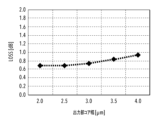
図6は、PLC100A及びPD6の結合時に測定されるPD6のチャネル毎の光電流から受光感度を求め、上記距離d[μm]に対する光結合損失Lоss[dB]を算出した結果を示すものである。尚、ここでは、PD6の単体の受光感度から距離d[μm]に対する光結合損失Lоss[dB]を算出した結果を、従来の溝部無しの場合を含めて得たとする。 FIG. 6 shows the results of calculating the optical coupling loss Loss [dB] with respect to the distance d [μm] by determining the light receiving sensitivity from the photocurrent of each channel of the PD 6 measured when the PLC 100A and the PD 6 are coupled. Here, it is assumed that the results of calculating the optical coupling loss Loss [dB] with respect to the distance d [μm] from the light receiving sensitivity of the PD 6 alone are obtained including the conventional case without a groove portion.

図6からは、溝部無しの場合、1dB弱の光結合損失が生じていることが判る。これに対し、光導波路2の出口領域E2側に溝部40を設けた場合、コア3の側面と溝部40の直線状凹部40bの側面との距離d=3μm~2μmの間で僅かに光結合損失が減少し、更に距離dを低減して0μmとしたとき、約0.5dBまで光結合損失を低減できることが判る。このような溝部40の構造は、図1に示したような従来の溝部無しの光導波路2にそのまま導入することが可能であり、光導波路2におけるモードフィールド径を、複雑な構造を導入することなく簡便に小さくできることを示す。 From FIG. 6, it can be seen that without the groove, an optical coupling loss of a little less than 1 dB occurs. On the other hand, when the groove 40 is provided on the exit region E2 side of the optical waveguide 2, there is a slight optical coupling loss between the side surface of the core 3 and the side surface of the linear recess 40b of the groove 40 in the distance d=3 μm to 2 μm. It can be seen that when the distance d is further reduced to 0 μm, the optical coupling loss can be reduced to about 0.5 dB. Such a structure of the groove 40 can be directly introduced into the conventional optical waveguide 2 without a groove as shown in FIG. 1, and the mode field diameter in the optical waveguide 2 can be changed by introducing a complicated structure. This shows that it can be easily made smaller.

以上の結果からは、PLC100A及びPD6の結合時にモードフィールド径が小さい光導波路のPD6への突き合わせ結合を実施しても、光結合損失を低減できることが判った。即ち、実施形態1に係る光導波路部品10Aと光素子20との結合時における光結合損失の低減効果、更には光導波路部品10Aを適用したPLC100A及びPD6の結合時における光結合損失の低減効果を確認できた。従って、実施形態1に係る光導波路部品10Aは、光素子20を結合してのハイブリッド集積により光電子集積型デバイスを構成するとき、低光結合損失で簡便に光導波路同士を結合し得る。このため、より低光損失が要求される光デバイスへの適用が有効になる。 From the above results, it was found that the optical coupling loss can be reduced even if an optical waveguide with a small mode field diameter is butt-coupled to the PD 6 when the PLC 100A and the PD 6 are coupled. That is, the effect of reducing the optical coupling loss when coupling the optical waveguide component 10A and the optical element 20 according to the first embodiment, and the effect of reducing the optical coupling loss when coupling the PLC 100A and the PD 6 to which the optical waveguide component 10A is applied. It could be confirmed. Therefore, the optical waveguide component 10A according to the first embodiment can easily couple the optical waveguides with each other with low optical coupling loss when forming an optoelectronic integrated device through hybrid integration by coupling the optical elements 20. Therefore, the present invention can be effectively applied to optical devices that require lower optical loss.

要するに、実施形態1に係る光導波路部品10Aでは、光導波路2のコア3の両側にコア3よりも深い溝部4が、コア3を覆う光導波路2の延在する方向に沿って並設されている。そして、これらの溝部4を占める媒質の屈折率をアンダークラッド2a及びオーバークラッド2bの屈折率よりも低くし、等価的にコア3とアンダークラッド2a及びオーバークラッド2bとの間の屈折率差を大きくしている。これにより、光導波路2のコア3を伝搬する光の閉じ込めを強くすることが可能となり、伝搬する光のモードフィールドを小さくする方向に調整を行うことができる。この結果、上記作用効果を奏するようになる。 In short, in the optical waveguide component 10A according to the first embodiment, grooves 4 deeper than the core 3 are arranged on both sides of the core 3 of the optical waveguide 2 in parallel along the direction in which the optical waveguide 2 covers the core 3. There is. Then, the refractive index of the medium occupying these grooves 4 is made lower than the refractive index of the undercladding 2a and overcladding 2b, and equivalently, the difference in refractive index between the core 3 and the undercladding 2a and overcladding 2b is increased. are doing. Thereby, it becomes possible to strengthen the confinement of the light propagating through the core 3 of the optical waveguide 2, and adjustment can be made in the direction of reducing the mode field of the propagating light. As a result, the above effects can be achieved.

(実施形態2)
図7は、本発明の実施形態2に係るPLC100Bと光素子20の適用例であるPD6´との光学的結合の様子を示した斜視図である。このPLC100Bは、PLC100Aと比べ、光導波路2´の多重構造のコア3″のチャネル数、溝部4´の総数が増設され、光導波路2´と基板1の端面との成す角度θを傾けて設定した点が相違している。即ち、このPLC100Bでは、光導波路2´の多重構造のコア3″が5チャネル分、溝部4´の総計が10個に増設され、光導波路2´のコア3″と基板1の端面との成す角度θが90度を基準とした場合、8度傾いて設定される。また、PD6´の光入力用とする光導波路も、同じ傾きで設定されている。
(Embodiment 2)
FIG. 7 is a perspective view showing how the PLC 100B according to Embodiment 2 of the present invention and a PD 6', which is an application example of the optical element 20, are optically coupled. Compared to PLC 100A, this PLC 100B has an increased number of channels in the core 3'' of the multiplexed structure of the optical waveguide 2' and a total number of grooves 4', and is set by tilting the angle θ formed by the optical waveguide 2' and the end surface of the substrate 1. That is, in this PLC 100B, the core 3'' of the optical waveguide 2' has a multiplex structure for 5 channels, the total number of grooves 4' is increased to 10, and the core 3'' of the optical waveguide 2' When the angle θ formed by the end face of the substrate 1 and the end face of the substrate 1 is set to be inclined by 8 degrees, when 90 degrees is a reference, the optical waveguide for optical input of the PD 6' is also set to have the same inclination.

このPLC100Bにおける溝部4´の構造は、図4を参照して説明した溝部40の構造とは細部が相違しており、全長750μmで光出力側の基板1の端面まで貫通しており、壁部を持たない構造となっている。但し、溝部4´の形状は、テーパ状凹部4a´及び直線状凹部4b´が繋がって形成され、基板1の端面と反対側の最も隔てられたテーパ状凹部4a´の端部で幅が最小となっている点は同じである。尚、ここでも基板1の水平方向における光導波路2´のコア3″の側面とコア3″の両側に設けられた溝部4´の側面との距離は、コア3″の幅に基づいて規定することができる。係る距離についても、コア3″の延在方向と垂直な方向におけるコア3″の幅の1/2以下であり、且つ零よりも大きいことが好ましい。 The structure of the groove 4' in this PLC 100B is different in detail from the structure of the groove 40 described with reference to FIG. It has a structure that does not have However, the shape of the groove 4' is formed by connecting the tapered recess 4a' and the linear recess 4b', and the width is the smallest at the end of the tapered recess 4a' that is farthest away from the end surface of the substrate 1. They are the same. In this case, the distance between the side surface of the core 3'' of the optical waveguide 2' and the side surface of the groove 4' provided on both sides of the core 3'' in the horizontal direction of the substrate 1 is defined based on the width of the core 3''. This distance is also preferably 1/2 or less of the width of the core 3'' in the direction perpendicular to the direction in which the core 3'' extends, and is greater than zero.

図8は、図7に示すPLC100Bの光導波路2´における出口領域E2側の細部構造を一部破断して示した斜視図である。この溝部4´の場合も、テーパ状凹部4a´及び直線状凹部4b´を有する形状であり、直線状凹部4b´が250μm、テーパ状凹部4a´が500μmの長さで形成され、クラッド材料の屈折率よりも低い空気で満たされている。但し、これらのテーパ状凹部4a´及び直線状凹部4b´の寸法形状は、あくまでも一例であり、任意に変更することが可能である。 FIG. 8 is a partially cutaway perspective view showing a detailed structure on the exit region E2 side of the optical waveguide 2' of the PLC 100B shown in FIG. The groove 4' also has a tapered recess 4a' and a linear recess 4b', with the linear recess 4b' having a length of 250 μm and the tapered recess 4a' having a length of 500 μm. It is filled with air whose refractive index is lower than its refractive index. However, the dimensions and shapes of these tapered recesses 4a' and linear recesses 4b' are merely examples, and can be arbitrarily changed.

更に、多重構造のコア3″は、コア3のS字型部から延びて端部となる直線部分の箇所に2重構造を成すテーパ形状の角板状部3a″と直線角板状部3b″とを結合した3重構造として構成される。コア3″の直線角板状部3b″の側面と溝部4´の直線状凹部4b´の側面との距離dは、一定の1.5μmにしている。尚、溝部4´の直線状凹部4b´における幅Wは、50μmとしている。ここで、コア3″の側面に存在するオーバークラッド2bをエッチングすれば、溝部4´の幅Wが規定されない構造についても具現し得る。しかし、PD6´との突き合せ結合を行う際にコア3″を含む光結合端面が接触により破損することを防ぐ役割を考慮すれば、光結合端面でコア3″の両側に溝部4´を介してクラッドが残る構造とする方が望ましい。この光導波路2´も、光回路領域から溝部4´の設けられた光結合端面の入出力領域に至る箇所において、コア3″の両側に溝部4´が無い構造を有し、且つ入出力領域でコア3″の両側の溝部4´を介してクラッドが残る構造を有する。要するに、光導波路2´の光回路領域は、必要な部分だけに溝部4´が設けられ、全ての領域のコア3″の両側に溝部4´が設けられる訳ではない。この点については、実施形態1に係る光導波路2についても同様である。 Furthermore, the core 3'' having a multiple structure has a tapered square plate-like part 3a'' and a straight square plate-like part 3b forming a double structure at the straight part extending from the S-shaped part of the core 3 and serving as an end. The distance d between the side surface of the straight rectangular plate-like portion 3b'' of the core 3'' and the side surface of the linear recess 4b' of the groove portion 4' is set to a constant 1.5 μm. Note that the width W of the linear recess 4b' of the groove 4' is set to 50 μm.Here, if the over cladding 2b existing on the side surface of the core 3'' is etched, the width W of the groove 4' becomes regulated. It is also possible to implement structures that are not However, if we consider the role of preventing the optical coupling end surface including the core 3'' from being damaged due to contact when butt-coupling with the PD6', it is necessary to install grooves 4' on both sides of the core 3'' at the optical coupling end surface. It is desirable to have a structure in which the cladding remains. This optical waveguide 2' also has a structure in which there is no groove part 4' on both sides of the core 3'' in the area from the optical circuit area to the input/output area of the optical coupling end face provided with the groove part 4'. It has a structure in which the cladding remains through the grooves 4' on both sides of the core 3''. In short, in the optical circuit area of the optical waveguide 2', grooves 4' are provided only in necessary parts, and grooves 4' are not provided on both sides of the core 3'' in all areas. The same applies to the optical waveguide 2 according to the first embodiment.

また、基板1の端面の反対側方向に向け、コア3″の直線角板状部3b″及び角板状部3a″の側面と溝部4´のテーパ状凹部4a´の側面との距離dが次第に大きくなるように、溝部4´のテーパ状凹部4a´のテーパ構造を設定している。このコア3″の側面と溝部4´のテーパ状凹部4a´の側面との距離dは、基板1の端面の反対側方向におけるテーパ状凹部4a´の端部で最大値を示す10μmとなっている。 Further, in the direction opposite to the end surface of the substrate 1, the distance d between the side surfaces of the straight rectangular plate-like portion 3b'' and the rectangular plate-like portion 3a'' of the core 3'' and the side surface of the tapered recess 4a' of the groove portion 4' is The taper structure of the tapered recess 4a' of the groove 4' is set to gradually increase in size.The distance d between the side surface of the core 3'' and the side surface of the tapered recess 4a' of the groove 4' is The maximum value is 10 μm at the end of the tapered recess 4a' in the direction opposite to the end surface.

更に、溝部4´のテーパ状凹部4a´の領域範囲内で、基板1の水平方向におけるコア3″の幅についても、直線角板状部3b″の一定の幅4.5μmから直線角板状部3b″に結合される角板状部3a″にテーパ構造を採用している。即ち、角板状部3a″では、直線角板状部3b″との結合箇所へ向けて、次第に小さくなるようにテーパ構造を採用している。 Furthermore, within the range of the tapered recess 4a' of the groove 4', the width of the core 3'' in the horizontal direction of the substrate 1 is changed from the constant width of 4.5 μm of the rectangular plate-shaped portion 3b'' to the linear rectangular plate-shaped portion 3b''. A tapered structure is adopted for the square plate-shaped portion 3a'' that is coupled to the portion 3b''. That is, the rectangular plate-like portion 3a'' adopts a tapered structure so that it gradually becomes smaller toward the joining location with the straight rectangular plate-like portion 3b''.

加えて、コア3″のテーパ構造を採用した角板状部3a″から直線角板状部3b″にかけてのコア3″の基板1の垂直方向における高さh1を3μmとしている。この高さh1は、図8中に示される2重構造に結合されるコア3の高さh=4.5μmよりも低く設定される。また、高さh1は、PD6´のコア3´の高さよりも小さいことが望ましい。係る2段の高さを有するコア″の3重構造は、通常高さhのコア3を形成した後、2重構造を成す角板状部3a″のテーパ構造と直線角板状部3b″とを形成する領域以外をマスクしてドライエッチングする工程を追加すれば形成できる。これは追加工程を要するものの、直線角板状部3b″周囲のアンダークラッド2bも同時にエッチングされるため、その後の溝部4´を形成する際のドライエッチングにおけるエッチング時間を短縮できるという副次的な効果をもたらす。 In addition, the height h1 of the core 3'' in the vertical direction of the substrate 1 from the rectangular plate-like portion 3a'' to the straight rectangular plate-like portion 3b'' which adopts the tapered structure of the core 3'' is set to 3 μm. This height h1 is set lower than the height h=4.5 μm of the core 3 coupled to the double structure shown in FIG. Moreover, it is desirable that the height h1 is smaller than the height of the core 3' of the PD 6'. Such a triple structure of a core'' having a two-stage height is usually achieved by forming a core 3 having a height h, and then forming a tapered structure of a rectangular plate-shaped portion 3a'' and a straight rectangular plate-shaped portion 3b'' forming a double structure. It can be formed by adding a step of dry etching while masking the area other than the area where the . A secondary effect is that the etching time in dry etching when forming the groove portion 4' can be shortened.

その他、PLC100Bでは、コア3″の結合界面からの反射戻り光を抑制するため、光導波路2´のコア3″と基板1の端面との成す角度θ(基準90度)=8度として、傾いた設定にした。そして、図7に示す5チャネル分のコア3″について、出口領域E2側のコア3″の直線角板状部3b″の幅を2~4μmとして設定した。 In addition, in the PLC 100B, in order to suppress the reflected return light from the coupling interface of the core 3'', the angle θ (reference 90 degrees) between the core 3'' of the optical waveguide 2' and the end surface of the substrate 1 is set to 8 degrees. I set it to the same setting. Regarding the core 3'' for 5 channels shown in FIG. 7, the width of the straight rectangular plate-like portion 3b'' of the core 3'' on the exit region E2 side was set to 2 to 4 μm.

このような構造のPLC100Bに突き合わせ結合するPD6´は、8度傾いた光導波路にスポットサイズ変換器が設けられる。図7を参照して、具体的に説明すれば、光強度分布の強度が1/eとなる全幅のモードフィールド径がチップの垂直方向及び水平方向に対してそれぞれ3μmとなるコア3´が光入力用とされ、光電変換部3c´に結合される。スポットサイズ変換器を介してコア3´に入力された光は、PD6´の8度傾いた光導波路を伝搬し、光電変換部3c´で電気信号に変換される。尚、光結合損失を除いたPD6´の単体での受光感度は波長1.55μmで1.0A/Wである。The PD 6' which is butt-coupled to the PLC 100B having such a structure is provided with a spot size converter in an optical waveguide inclined at 8 degrees. To explain specifically with reference to FIG. 7, the core 3' has a mode field diameter of 3 μm in the vertical and horizontal directions of the chip, in which the intensity of the light intensity distribution is 1/e 2 and the mode field diameter in the full width is 3 μm. It is used for optical input and is coupled to the photoelectric conversion section 3c'. The light input to the core 3' via the spot size converter propagates through the optical waveguide inclined at 8 degrees of the PD 6', and is converted into an electrical signal by the photoelectric conversion section 3c'. Note that the light receiving sensitivity of the PD 6' alone, excluding optical coupling loss, is 1.0 A/W at a wavelength of 1.55 μm.

PLC100Bに対するPD6´の突き合わせ結合に先立って、PLC100Bの出口領域E2側のコア3″の直線角板状部3b″の側面の溝部4´にシリコーン樹脂を充填する。これにより固着・硬化させた後、ダイシング、研磨等によって、接続面を形成する。PD6´の突き合わせ結合は、PLC100Bのコア3″の直線角板状部3b″から出力される光に対し、PD6´の受光感度が最大になるように、PLC100Bの光導波路2´とPD6´の光導波路との位置をアライメントする。そして、PLC100Bのコア3″とアンダークラッド2a及びオーバークラッド2bとの屈折率に近い赤外領域で透明な樹脂をPLC100B及びPD6´間に充填する。そして、樹脂の硬化による固着・固定を行う。このようにして、光電子集積型デバイスを構成することができる。但し、ここでも、PD6´の光導波路となる端面には、充填する樹脂の屈折率に対応した反射防止膜を設けることが好ましい。 Prior to the butt connection of the PD 6' to the PLC 100B, a silicone resin is filled into the groove 4' on the side surface of the straight rectangular plate-like portion 3b'' of the core 3'' on the outlet area E2 side of the PLC 100B. After this fixation and hardening, a connection surface is formed by dicing, polishing, etc. The butt-coupling of the PD6' is performed by connecting the optical waveguide 2' and the PD6' of the PLC 100B so that the light receiving sensitivity of the PD6' is maximized for the light output from the straight rectangular plate-like portion 3b'' of the core 3'' of the PLC 100B. Align the position with the optical waveguide. Then, a transparent resin in an infrared region close to the refractive index of the core 3'' of the PLC 100B and the under cladding 2a and over cladding 2b is filled between the PLC 100B and the PD 6'.Fixation and fixation are performed by curing the resin. In this way, an optoelectronic integrated device can be constructed.However, here as well, it is preferable to provide an antireflection film corresponding to the refractive index of the resin to be filled on the end face of the PD 6' that will become an optical waveguide.

樹脂による固定後に樹脂を外せば、溝部4´内に樹脂が入り込むことを抑制しつつ、固定を行うことができる。ここでは、シリコーン樹脂を用いて、固定後に外す場合を例示できる。但し、アンダークラッド2a及びオーバークラッド2bよりも屈折率の低い樹脂を用いて溝部4´を充填した場合には、固定後に樹脂を外さなくても良い。 If the resin is removed after fixation with the resin, the fixation can be performed while suppressing the resin from entering into the groove 4'. Here, a case where a silicone resin is used and is removed after fixation can be exemplified. However, if the groove 4' is filled with a resin having a lower refractive index than the under cladding 2a and over cladding 2b, it is not necessary to remove the resin after fixing.

実施形態2に係るPLC100Bでは、充填する樹脂による光導波路2´のコア3″の汚染を防ぐため、コア3″が露出しないように出口領域E2側のコア3″の直線角板状部3b″と溝部4´との間の距離dを1.5μmとした。尚、コア3″が露出する構造は、水分等の影響によりコア3″の屈折率が変動し、特性劣化を引き起こす虞がある。このため、信頼性上の観点から、コア3″の直線角板状部3b″と溝部4´との間の距離dを零にしないことが望ましい。こうした構造とするためには、予めコア3″側面にクラッドが残るように溝部4´を形成する手法、溝部4´の形成後にCVD法、スパッタ法等によりSiO等の材料で表面保護膜を形成する手法等を適用させることができる。In the PLC 100B according to the second embodiment, in order to prevent the core 3'' of the optical waveguide 2' from being contaminated by the resin to be filled, the straight rectangular plate-shaped portion 3b'' of the core 3'' on the exit area E2 side is removed so that the core 3'' is not exposed. The distance d between the groove portion 4' and the groove portion 4' was set to 1.5 μm. Note that in a structure in which the core 3'' is exposed, the refractive index of the core 3'' changes due to the influence of moisture, etc., and there is a possibility that the characteristics may deteriorate. Therefore, from the viewpoint of reliability, it is desirable that the distance d between the straight rectangular plate-like portion 3b'' of the core 3'' and the groove portion 4' not become zero. In order to achieve such a structure, the method is to form the groove 4' in advance so that the cladding remains on the side surface of the core 3'', and after forming the groove 4', to apply a surface protective film using a material such as SiO 2 by CVD, sputtering, etc. A forming method etc. can be applied.

図9は、PLC100Bに光を入力し、光導波路2´の基板1の端面におけるモードフィールド径[μm]をチャネル毎に測定した結果を、出口領域E2側のコア3の幅[μm]との対応関係で示した図である。尚、ここではPLC100Bに対し、波長1.55μmの光をファイバで入力したものとする。 FIG. 9 shows the result of inputting light into the PLC 100B and measuring the mode field diameter [μm] at the end surface of the substrate 1 of the optical waveguide 2' for each channel, and the relationship between the width [μm] of the core 3 on the exit region E2 side. It is a diagram shown in correspondence. Here, it is assumed that light with a wavelength of 1.55 μm is input to the PLC 100B through a fiber.

図9からは、基板1の垂直方向におけるモードフィールド径は、3重構造のコア3″の2重構造部の高さh1を3μmとしたことにより、コア3の高さhの4.5μmのときから小さくなり、約4.0μmとなったことが判る。また、コア3″の幅の減少に対し、基板1の垂直方向におけるモードフィールド径は、3.9μmから4.1μmまで僅かに大きくなった。これに対し、基板1の水平方向のモードフィールド径は、4.4μmから3.2μmまで大幅に小さくなった。こうした結果から、PLC100Bでは、溝部無しの場合と比較して、水平方向及び垂直方向のモードフィールド径が小さくなり、PD6´の光入力用の光導波路のモードフィールド径に近付けられることが判った。 From FIG. 9, it can be seen that the mode field diameter in the vertical direction of the substrate 1 is 4.5 μm when the height h of the core 3 is set to 3 μm because the height h1 of the double structure portion of the triple structure core 3″ is set to 3 μm. It can be seen that the diameter of the mode field in the vertical direction of the substrate 1 slightly increased from 3.9 μm to 4.1 μm in response to the decrease in the width of the core 3″. became. On the other hand, the horizontal mode field diameter of the substrate 1 was significantly reduced from 4.4 μm to 3.2 μm. From these results, it was found that in the PLC 100B, the mode field diameter in the horizontal and vertical directions is smaller than in the case without the groove, and can be brought closer to the mode field diameter of the optical waveguide for optical input of the PD 6'.

図10は、PLC100B及びPD6´の結合時に測定されるPD6´のチャネル毎の光電流から受光感度を求め、上記出口領域E2におけるコア3″の幅に対する光結合損失Lоss[dB]を算出した結果を示すものである。尚、ここではPD6の単体の受光感度から光結合損失Lоss[dB]を算出した結果を得たものとする。 FIG. 10 shows the results of calculating the optical coupling loss Lоss [dB] with respect to the width of the core 3'' in the exit region E2 by determining the light receiving sensitivity from the photocurrent for each channel of the PD6' measured when the PLC100B and the PD6' are coupled. Here, it is assumed that the optical coupling loss Loss [dB] has been calculated from the light receiving sensitivity of the PD 6 alone.

図10からは、コア3″の幅4μmでは0.9dB程あった光結合損失が、コア3″の幅を2.5μm以下とすることで、0.7dB以下まで低減させられることが判った。実施形態1では、コア3の側面と溝部40の直線状凹部40bの側面との距離dが1μmでも0.8dB程度までの光結合損失の低減であったのに対し、実施形態2の構造を適用すれば、更に光結合損失を低減させることができる。即ち、実施形態2の構造の特徴は、コア3″の側面が外環境に晒されないように、コア3″及び溝部4´間に薄いクラッドが設けられた構造である。 From Figure 10, it was found that the optical coupling loss, which was approximately 0.9 dB when the width of the core 3'' was 4 μm, was reduced to 0.7 dB or less by making the width of the core 3'' 2.5 μm or less. . In the first embodiment, the optical coupling loss was reduced to about 0.8 dB even when the distance d between the side surface of the core 3 and the side surface of the linear recess 40b of the groove 40 was 1 μm, whereas the structure of the second embodiment If applied, the optical coupling loss can be further reduced. That is, the structure of the second embodiment is characterized in that a thin cladding is provided between the core 3'' and the groove 4' so that the side surface of the core 3'' is not exposed to the outside environment.

実施形態2の構造による光結合損失の効果は、PLC100Bの光導波路2´のコア3″の多重構造における高さ変更によるモードフィールド径の変換損失の低減(約0.5dB)を含んでいる。この損失を低減する光導波路2´の構造(コア3″の多重構造)を導入することにより、更に光結合損失を低減させることができる。これらの結果より、実施形態2に係る光結合損失の低減効果を確認できた。 The effect of the optical coupling loss due to the structure of the second embodiment includes a reduction (about 0.5 dB) in the conversion loss of the mode field diameter due to the height change in the multiplex structure of the core 3'' of the optical waveguide 2' of the PLC 100B. By introducing a structure of the optical waveguide 2' (multiplex structure of core 3'') that reduces this loss, the optical coupling loss can be further reduced. From these results, the effect of reducing optical coupling loss according to the second embodiment was confirmed.

更に、実施形態2の構造による光結合損失の効果は、光導波路2´の多重構造のコア3″の結合に伴う反射戻り光の発生防止を含んでいる。即ち、使用する各部の材料、光導波路2´の設計の違いにより、光導波路部品と光素子との間には屈折率差が生じる。特に、屈折率界面で発生する反射の影響、突き合わせ結合では光結合距離が短いため、通信用デバイスとして好ましくない反射戻り光が発生し易い。これは、屈折率界面で反射した光が光導波路部品に戻る際に、その一部が光導波路2´に結合することで発生する。反射戻り光は、光信号の伝送品質に大きく影響することから、特に光導波路部品を光通信システムに適用する場合、30~40dB以上損失させることが求められる。この反射戻り光を低減するため、実施形態2の構造では、基板1の端面の垂直方向に対する光導波路2´の角度θを8度にしている。尚、上述した角度θは、8度以上であれば良いが、あくまでも多重構造のコア3″の結合に伴う反射戻り光の発生防止を意図するものであり、必要以上に過度な傾斜を示すものではない。 Furthermore, the effect of optical coupling loss due to the structure of Embodiment 2 includes prevention of the occurrence of reflected return light due to the coupling of the core 3'' of the multiple structure of the optical waveguide 2'. Due to the difference in the design of the waveguide 2', a refractive index difference occurs between the optical waveguide component and the optical element.In particular, due to the influence of reflection occurring at the refractive index interface and the short optical coupling distance in butt coupling, it is difficult to use for communications. Reflected return light, which is undesirable for the device, is likely to occur.This occurs because when the light reflected at the refractive index interface returns to the optical waveguide component, a part of it is coupled to the optical waveguide 2'.Reflected return light Since this greatly affects the transmission quality of optical signals, especially when applying optical waveguide components to optical communication systems, it is required to reduce the loss by 30 to 40 dB or more.In order to reduce this reflected return light, Embodiment 2 In this structure, the angle θ of the optical waveguide 2' with respect to the vertical direction of the end surface of the substrate 1 is set to 8 degrees.The above-mentioned angle θ may be 8 degrees or more, but it is limited to the core 3'' of the multiplex structure. This is intended to prevent the occurrence of reflected return light due to the combination of the two, and does not exhibit an excessive slope more than necessary.

以上に説明したように、実施形態2に係るPLC100Bでは、実施形態1で説明した構成に加え、光導波路2´の多重構造のコア3″における高さ変更、基板1の端面の垂直方向に対する光導波路2´の傾斜角設定を導入している。この結果、光導波路を有する光素子を結合してのハイブリッド集積により光電子集積型デバイスを構成するとき、実施形態1の場合よりも低光結合損失で簡便に光導波路同士を結合できる。従って、より低光損失が要求される光デバイスへの適用が一層有効になる。 As described above, in addition to the configuration described in Embodiment 1, the PLC 100B according to Embodiment 2 includes a height change in the core 3'' of the multiple structure of the optical waveguide 2', and an optical guide in the vertical direction of the end surface of the substrate 1. The inclination angle setting of the wave path 2' is introduced.As a result, when an optoelectronic integrated device is constructed by hybrid integration by coupling optical elements having optical waveguides, the optical coupling loss is lower than in the case of Embodiment 1. Optical waveguides can be easily coupled with each other. Therefore, the application to optical devices that require lower optical loss becomes more effective.

Claims (4)

基板の主面上に光導波路が備えられ、当該光導波路は、積層されたアンダークラッドと、コアと、オーバークラッドと、を有すると共に、当該基板の端面付近に結合される光素子との間で信号を入出力可能な光導波路部品であって、
前記基板の水平方向における前記端面付近の前記光導波路の前記コアの両側に、当該基板の垂直方向に対して断面方向で前記コアよりも深く形成され、当該コアを覆う当該光導波路の延在方向に沿って並設された溝部を有し、
前記溝部を占める媒質の屈折率は、前記アンダークラッド及び前記オーバークラッドの屈折率よりも低く、
前記基板の水平方向における前記光導波路の前記コアの側面と当該コアの両側に設けられた前記溝部の側面との距離が、当該コアの延在方向と垂直な方向における当該コアの幅の1/2以下であり、且つ零よりも大きく、
前記基板の前記光導波路の両側に設けられた前記溝部は、当該基板の端面まで貫通せずに当該端面からオフセットした箇所まで形成され、壁を有することを特徴とする光導波路部品。
An optical waveguide is provided on the main surface of the substrate, and the optical waveguide includes a laminated undercladding, a core, and an overcladding, and has an optical waveguide connected to an optical element coupled near the end surface of the substrate. An optical waveguide component that can input and output signals,
The optical waveguide is formed on both sides of the core of the optical waveguide near the end surface in the horizontal direction of the substrate, deeper than the core in the cross-sectional direction with respect to the vertical direction of the substrate, and covers the core in the extending direction of the optical waveguide. It has grooves arranged in parallel along the
The refractive index of the medium occupying the groove portion is lower than the refractive index of the under cladding and the over cladding,
The distance between the side surface of the core of the optical waveguide in the horizontal direction of the substrate and the side surface of the groove provided on both sides of the core is 1/1 of the width of the core in the direction perpendicular to the extending direction of the core. 2 or less and greater than zero,
An optical waveguide component, wherein the grooves provided on both sides of the optical waveguide of the substrate do not penetrate to the end surface of the substrate, but are formed to a location offset from the end surface, and have walls.
基板の主面上に光導波路が備えられ、当該光導波路は、積層されたアンダークラッドと、コアと、オーバークラッドと、を有すると共に、当該基板の端面付近に結合される光素子との間で信号を入出力可能な光導波路部品であって、An optical waveguide is provided on the main surface of the substrate, and the optical waveguide includes a laminated undercladding, a core, and an overcladding, and has an optical waveguide connected to an optical element coupled near the end surface of the substrate. An optical waveguide component that can input and output signals,
前記基板の水平方向における前記端面付近の前記光導波路の前記コアの両側に、当該基板の垂直方向に対して断面方向で前記コアよりも深く形成され、当該コアを覆う当該光導波路の延在方向に沿って並設された溝部を有し、The optical waveguide is formed on both sides of the core of the optical waveguide near the end surface in the horizontal direction of the substrate, deeper than the core in the cross-sectional direction with respect to the vertical direction of the substrate, and covers the core in the extending direction of the optical waveguide. It has grooves arranged in parallel along the
前記溝部を占める媒質の屈折率は、前記アンダークラッド及び前記オーバークラッドの屈折率よりも低く、The refractive index of the medium occupying the groove portion is lower than the refractive index of the under cladding and the over cladding,
前記基板の水平方向における前記光導波路の前記コアの側面と当該コアの両側に設けられた前記溝部の側面との距離が、当該コアの延在方向と垂直な方向における当該コアの幅の1/2以下であり、且つ零よりも大きく、The distance between the side surface of the core of the optical waveguide in the horizontal direction of the substrate and the side surface of the groove provided on both sides of the core is 1/1 of the width of the core in the direction perpendicular to the extending direction of the core. 2 or less and greater than zero,
前記光導波路は、光回路領域から前記溝部の設けられた光結合端面の入出力領域に至る箇所において、前記コアの両側に当該溝部が無い構造を有し、且つ当該入出力領域で当該コアの両側の当該溝部を介して前記アンダークラッド及び前記オーバークラッドの少なくとも何れかによるクラッドが残る構造を有することを特徴とする光導波路部品。The optical waveguide has a structure in which there is no groove on both sides of the core at a location extending from the optical circuit region to the input/output region of the optical coupling end surface provided with the groove, and where the groove is absent from the core in the input/output region. An optical waveguide component having a structure in which a cladding formed by at least one of the undercladding and the overcladding remains through the groove portions on both sides.
前記基板の水平方向における前記光導波路の前記コアの側面と当該コアの両側に設けられた前記溝部の側面との距離が、当該基板の端面の反対方向から当該端面の方向に向かって小さくなるように、当該溝部にテーパ形状を持たせた
ことを特徴とする請求項1または2に記載の光導波路部品。
The distance between the side surface of the core of the optical waveguide and the side surface of the groove provided on both sides of the core in the horizontal direction of the substrate becomes smaller from the direction opposite to the end surface of the substrate toward the end surface. The optical waveguide component according to claim 1 or 2, wherein the groove portion has a tapered shape.
前記基板の水平方向における前記光導波路と当該基板の端面との成す角度が90度を基準とした場合、8度以上傾いている
ことを特徴とする請求項1乃至3のいずれか1項に記載の光導波路部品。
According to any one of claims 1 to 3, the angle between the optical waveguide and the end face of the substrate in the horizontal direction of the substrate is inclined by 8 degrees or more with respect to 90 degrees. optical waveguide components.
JP2021543840A 2019-09-03 2019-09-03 Optical waveguide parts Active JP7356048B2 (en)

Applications Claiming Priority (1)

Application Number Priority Date Filing Date Title
PCT/JP2019/034620 WO2021044517A1 (en) 2019-09-03 2019-09-03 Optical waveguide component

Publications (2)

Publication Number Publication Date
JPWO2021044517A1 JPWO2021044517A1 (en) 2021-03-11
JP7356048B2 true JP7356048B2 (en) 2023-10-04

Family

ID=74852345

Family Applications (1)

Application Number Title Priority Date Filing Date
JP2021543840A Active JP7356048B2 (en) 2019-09-03 2019-09-03 Optical waveguide parts

Country Status (3)

Country Link
US (1) US20220334309A1 (en)
JP (1) JP7356048B2 (en)
WO (1) WO2021044517A1 (en)

Citations (7)

* Cited by examiner, † Cited by third party
Publication number Priority date Publication date Assignee Title
JP2002006168A (en) 2000-06-26 2002-01-09 Furukawa Electric Co Ltd:The Optical waveguide module
JP2005301301A (en) 2005-05-23 2005-10-27 Nec Corp Optical coupler
JP2006017914A (en) 2004-06-30 2006-01-19 Tdk Corp Composite optical fiber and fiber array
JP2007079225A (en) 2005-09-15 2007-03-29 Nippon Telegr & Teleph Corp <Ntt> Connecting method of wavelength conversion element and connecting member
US20070153858A1 (en) 2006-01-03 2007-07-05 Samsung Electronics Co.; Ltd Optical spot size converter integrated laser device and method for manufacturing the same
JP2009031780A (en) 2007-06-26 2009-02-12 Panasonic Electric Works Co Ltd Optical module
JP2016161915A (en) 2015-03-05 2016-09-05 日本碍子株式会社 Optical waveguide device and optical device

Family Cites Families (1)

* Cited by examiner, † Cited by third party
Publication number Priority date Publication date Assignee Title
JPH05288944A (en) * 1992-04-15 1993-11-05 Sumitomo Electric Ind Ltd Optical waveguide and its production

Patent Citations (7)

* Cited by examiner, † Cited by third party
Publication number Priority date Publication date Assignee Title
JP2002006168A (en) 2000-06-26 2002-01-09 Furukawa Electric Co Ltd:The Optical waveguide module
JP2006017914A (en) 2004-06-30 2006-01-19 Tdk Corp Composite optical fiber and fiber array
JP2005301301A (en) 2005-05-23 2005-10-27 Nec Corp Optical coupler
JP2007079225A (en) 2005-09-15 2007-03-29 Nippon Telegr & Teleph Corp <Ntt> Connecting method of wavelength conversion element and connecting member
US20070153858A1 (en) 2006-01-03 2007-07-05 Samsung Electronics Co.; Ltd Optical spot size converter integrated laser device and method for manufacturing the same
JP2009031780A (en) 2007-06-26 2009-02-12 Panasonic Electric Works Co Ltd Optical module
JP2016161915A (en) 2015-03-05 2016-09-05 日本碍子株式会社 Optical waveguide device and optical device

Also Published As

Publication number Publication date
US20220334309A1 (en) 2022-10-20
WO2021044517A1 (en) 2021-03-11
JPWO2021044517A1 (en) 2021-03-11

Similar Documents

Publication Publication Date Title
US10656333B2 (en) Two-stage adiabatically coupled photonic systems
JP3749652B2 (en) Optical multiplexer / demultiplexer, optical waveguide module, and optical communication device
US7561765B2 (en) Optical integrated circuit and optical integrated circuit module
KR101639602B1 (en) Optical coupling/splitting device, two-way optical propagation device, and optical transmit-receive system
KR100893805B1 (en) Optical system including optical waveguide
US20100111468A1 (en) Optical integrated circuit and optical integrated circuit module
KR100897887B1 (en) Hybrid integration structure between optical active devices and planar lightwave circuit using fiber array
JP3434986B2 (en) Optical multiplexing / demultiplexing circuit
US7577328B2 (en) Optical reflector, optical system and optical multiplexer/demultiplexer device
US7024079B2 (en) Optical waveguide module
JP3344446B2 (en) Optical transceiver module
US8615146B2 (en) Planar optical waveguide
JP3703401B2 (en) Lightwave circuit module
JP7356048B2 (en) Optical waveguide parts
CN113589429A (en) Array waveguide grating based on auxiliary waveguide
US7289702B2 (en) Optical waveguide apparatus
US20230266534A1 (en) Optical Waveguide Device and Method for Manufacturing the Same
WO2020209284A1 (en) Optical waveguide component and manufacturing method therefor
Takato Recent progress on practical PLC devices for optical access systems and dense WDM systems
JP3897231B2 (en) Optical splitter
JP4792422B2 (en) Planar lightwave circuit
JP4648342B2 (en) Optical waveguide device

Legal Events

Date Code Title Description
A621 Written request for application examination

Free format text: JAPANESE INTERMEDIATE CODE: A621

Effective date: 20211224

A131 Notification of reasons for refusal

Free format text: JAPANESE INTERMEDIATE CODE: A131

Effective date: 20230110

A521 Request for written amendment filed

Free format text: JAPANESE INTERMEDIATE CODE: A523

Effective date: 20230207

A131 Notification of reasons for refusal

Free format text: JAPANESE INTERMEDIATE CODE: A131

Effective date: 20230516

A521 Request for written amendment filed

Free format text: JAPANESE INTERMEDIATE CODE: A523

Effective date: 20230621

TRDD Decision of grant or rejection written
A01 Written decision to grant a patent or to grant a registration (utility model)

Free format text: JAPANESE INTERMEDIATE CODE: A01

Effective date: 20230822

A61 First payment of annual fees (during grant procedure)

Free format text: JAPANESE INTERMEDIATE CODE: A61

Effective date: 20230904

R150 Certificate of patent or registration of utility model

Ref document number: 7356048

Country of ref document: JP

Free format text: JAPANESE INTERMEDIATE CODE: R150