JP3749652B2 - Optical multiplexer / demultiplexer, optical waveguide module, and optical communication device - Google Patents
Optical multiplexer / demultiplexer, optical waveguide module, and optical communication device Download PDFInfo
- Publication number
- JP3749652B2 JP3749652B2 JP2000187539A JP2000187539A JP3749652B2 JP 3749652 B2 JP3749652 B2 JP 3749652B2 JP 2000187539 A JP2000187539 A JP 2000187539A JP 2000187539 A JP2000187539 A JP 2000187539A JP 3749652 B2 JP3749652 B2 JP 3749652B2
- Authority
- JP
- Japan
- Prior art keywords
- optical
- light
- optical waveguide
- waveguide
- filter
- Prior art date
- Legal status (The legal status is an assumption and is not a legal conclusion. Google has not performed a legal analysis and makes no representation as to the accuracy of the status listed.)
- Expired - Fee Related
Links
Images


Classifications
-
- G—PHYSICS
- G02—OPTICS
- G02B—OPTICAL ELEMENTS, SYSTEMS OR APPARATUS
- G02B6/00—Light guides; Structural details of arrangements comprising light guides and other optical elements, e.g. couplings
- G02B6/24—Coupling light guides
- G02B6/26—Optical coupling means
- G02B6/28—Optical coupling means having data bus means, i.e. plural waveguides interconnected and providing an inherently bidirectional system by mixing and splitting signals
- G02B6/293—Optical coupling means having data bus means, i.e. plural waveguides interconnected and providing an inherently bidirectional system by mixing and splitting signals with wavelength selective means
- G02B6/29379—Optical coupling means having data bus means, i.e. plural waveguides interconnected and providing an inherently bidirectional system by mixing and splitting signals with wavelength selective means characterised by the function or use of the complete device
- G02B6/2938—Optical coupling means having data bus means, i.e. plural waveguides interconnected and providing an inherently bidirectional system by mixing and splitting signals with wavelength selective means characterised by the function or use of the complete device for multiplexing or demultiplexing, i.e. combining or separating wavelengths, e.g. 1xN, NxM
-
- G—PHYSICS
- G02—OPTICS
- G02B—OPTICAL ELEMENTS, SYSTEMS OR APPARATUS
- G02B6/00—Light guides; Structural details of arrangements comprising light guides and other optical elements, e.g. couplings
- G02B6/10—Light guides; Structural details of arrangements comprising light guides and other optical elements, e.g. couplings of the optical waveguide type
- G02B6/12—Light guides; Structural details of arrangements comprising light guides and other optical elements, e.g. couplings of the optical waveguide type of the integrated circuit kind
- G02B6/12007—Light guides; Structural details of arrangements comprising light guides and other optical elements, e.g. couplings of the optical waveguide type of the integrated circuit kind forming wavelength selective elements, e.g. multiplexer, demultiplexer
-
- G—PHYSICS
- G02—OPTICS
- G02B—OPTICAL ELEMENTS, SYSTEMS OR APPARATUS
- G02B6/00—Light guides; Structural details of arrangements comprising light guides and other optical elements, e.g. couplings
- G02B6/24—Coupling light guides
- G02B6/26—Optical coupling means
- G02B6/28—Optical coupling means having data bus means, i.e. plural waveguides interconnected and providing an inherently bidirectional system by mixing and splitting signals
- G02B6/2804—Optical coupling means having data bus means, i.e. plural waveguides interconnected and providing an inherently bidirectional system by mixing and splitting signals forming multipart couplers without wavelength selective elements, e.g. "T" couplers, star couplers
- G02B6/2808—Optical coupling means having data bus means, i.e. plural waveguides interconnected and providing an inherently bidirectional system by mixing and splitting signals forming multipart couplers without wavelength selective elements, e.g. "T" couplers, star couplers using a mixing element which evenly distributes an input signal over a number of outputs
- G02B6/2813—Optical coupling means having data bus means, i.e. plural waveguides interconnected and providing an inherently bidirectional system by mixing and splitting signals forming multipart couplers without wavelength selective elements, e.g. "T" couplers, star couplers using a mixing element which evenly distributes an input signal over a number of outputs based on multimode interference effect, i.e. self-imaging
-
- G—PHYSICS
- G02—OPTICS
- G02B—OPTICAL ELEMENTS, SYSTEMS OR APPARATUS
- G02B6/00—Light guides; Structural details of arrangements comprising light guides and other optical elements, e.g. couplings
- G02B6/24—Coupling light guides
- G02B6/26—Optical coupling means
- G02B6/28—Optical coupling means having data bus means, i.e. plural waveguides interconnected and providing an inherently bidirectional system by mixing and splitting signals
- G02B6/293—Optical coupling means having data bus means, i.e. plural waveguides interconnected and providing an inherently bidirectional system by mixing and splitting signals with wavelength selective means
- G02B6/29346—Optical coupling means having data bus means, i.e. plural waveguides interconnected and providing an inherently bidirectional system by mixing and splitting signals with wavelength selective means operating by wave or beam interference
- G02B6/29361—Interference filters, e.g. multilayer coatings, thin film filters, dichroic splitters or mirrors based on multilayers, WDM filters
- G02B6/29362—Serial cascade of filters or filtering operations, e.g. for a large number of channels
- G02B6/29364—Cascading by a light guide path between filters or filtering operations, e.g. fibre interconnected single filter modules
-
- G—PHYSICS
- G02—OPTICS
- G02B—OPTICAL ELEMENTS, SYSTEMS OR APPARATUS
- G02B6/00—Light guides; Structural details of arrangements comprising light guides and other optical elements, e.g. couplings
- G02B6/10—Light guides; Structural details of arrangements comprising light guides and other optical elements, e.g. couplings of the optical waveguide type
- G02B6/12—Light guides; Structural details of arrangements comprising light guides and other optical elements, e.g. couplings of the optical waveguide type of the integrated circuit kind
- G02B2006/12083—Constructional arrangements
- G02B2006/12109—Filter
-
- G—PHYSICS
- G02—OPTICS
- G02B—OPTICAL ELEMENTS, SYSTEMS OR APPARATUS
- G02B6/00—Light guides; Structural details of arrangements comprising light guides and other optical elements, e.g. couplings
- G02B6/24—Coupling light guides
- G02B6/26—Optical coupling means
- G02B6/30—Optical coupling means for use between fibre and thin-film device
-
- G—PHYSICS
- G02—OPTICS
- G02B—OPTICAL ELEMENTS, SYSTEMS OR APPARATUS
- G02B6/00—Light guides; Structural details of arrangements comprising light guides and other optical elements, e.g. couplings
- G02B6/24—Coupling light guides
- G02B6/42—Coupling light guides with opto-electronic elements
- G02B6/4201—Packages, e.g. shape, construction, internal or external details
- G02B6/4246—Bidirectionally operating package structures
Description
【0001】
【発明の属する技術分野】
本願発明は、光導波路を有する光システム、わけても、いわゆるマルチモード干渉( MMI:Multi−Mode Inteference)型光導波路を有する光システムに関するものである。本願発明によれば、極めて良好な光合分波器を提供することが出来る。
【0002】
【従来の技術】
最近のインターネットを始めとするマルチメディア通信の発展に伴い、高速・大容量通信に向けた光波長多重(WDM:Wavelength Division Multiplexing)技術の研究が盛んになっている。WDM通信システムを構築する上で重要となる光部品の1つに、複数の波長を有する光を合波もしくは分波する光合分波器がある。その中でも低コスト化・小型化かつ高機能化の観点から、基板上に石英(ガラス)やポリマ等から成る光導波路及び光合分波器を形成し光送受信器等を実装することで集積化を図る方法が注目されている。
【0003】
光合分波器としてはフィルタ型、方向性結合器型あるいはマッハツェンダー干渉器型等が知られている。更に、モジュールの小型化に有利なフィルタの型については、例えば、日本国公開特許公報、特開平8-190026号(記事1)に記載された技術が知られている。
【0004】
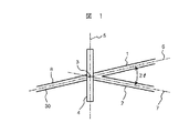
図1は上記記事1に示されたフィルタ型光合分波器である。この光合分波器は直線光導波路、1及び2を交差させ、その交差部に光学フィルタ4を設けている。この例では、光学フィルタ4の波長に対する透過および反射特性を利用してWDM信号を反射光と透過光に合分波する。即ち、本構造は、2θの角度で交差する2つの光導波路1と2の光軸の交点3が光学フィルタ4の等価的な反射中心面5上に合うように設計する必要がある。尚、図1において、光導波路1、2、および3の中心軸が各々符号6、7、及び8として示されている。
【0005】
【発明が解決しようとする課題】
本願発明が解決すべき課題の第1は、マルチモード干渉型光導波路内に反射手段、例えば代表的には光学フィルタを設置し、その反射光を利用する光システムにおける、前記反射手段の設置位置のずれに対するトレランスを小さくすることである。即ち、反射手段の設置位置のずれに基づく、当該マルチモード干渉型光導波路の光の伝達特性の変化を極力小さなものとすることである。反射手段による反射光を用いる場合、反射手段の位置のずれは、少なくとも入射光の当該反射手段までの距離の2倍の光路となる。この為、十分な伝搬特性を確保するに、この反射手段の設置位置のずれに対するトレランスを小さくすることが重要である。
【0006】
本願発明が解決すべき課題の第2は、マルチモード干渉型光導波路の相対する端面に設けた光導波路相互での光の漏れ光を防止することである。
【0007】
【課題を解決するための手段】
本願発明の第1の課題を解決する代表的な形態は、例えば、平面基板上に形成された複数の波長を有する信号光を合波または分波する光合分波器に供することが出来る。そして、本願発明によれば、前記第1および第2の課題を合わせて解決することを可能とする。
【0008】
本願発明の代表的な形態は、第1、第2、及び第3の光導波路と、マルチモードでの光の伝搬が可能な第4の光導波路と、前記第4の光導波路内の光の進行方向に交差して設けられた光学フィルタとを少なくとも有し、前記第1の光導波路が前記第4の光導波路の第1の端面に接続され、前記第2及び第3の各光導波路が前記第4の光導波路の前記第1の端面に対向する第2の端面の所定の個別位置に接続され、前記第4の光導波路の第1の端面および第2の端面は各々当該第4の光導波路内の光の進行方向と交差する端面であり、前記第4の光導波路は、前記第2および第3の光導波路のいずれかの光導波路からの第1の波長の光入力が前記第4の光導波路内の光の伝搬によって、前記光学フィルタを透過した上で前記第1の光導波路内に前記第1の波長の光入力に対応する光の伝搬を可能となし、且つ前記第2および第3の光導波路のいずれかの光導波路からの第2の波長の光入力が前記光学フィルタでの反射を介して、前記第2および第3の光導波路の内の光入力のない光導波路内に前記第2の波長の光入力に対応する光の伝搬を可能となす、マルチモードでの光の伝搬が可能な光導波路である光導波路を有する光システムである。
【0009】
以下に本願発明の原理を説明する。図7はマルチモード干渉型導波路における光の伝搬の状態を模式的に示したものである。マルチモード干渉型導波路10では、例えば第2の光導波路12から入射した信号光は前記マルチモード干渉型光導波路10において多モード光に分解される。図7には0次、1次及び2次のモードのみが示されて、より高次のモードは図示が省略されている。さらに励起された高次モード光はモード間で干渉し、前記マルチモード干渉型光導波路内に強度分布(干渉縞)を生じる。本願発明は、この現象を利用し、第2の光導波路12よりの入射光に対して、第1の光導波路11の入り口近傍での光の強度分布が山となるようにする。この構成によって、第2の光導波路12からの入射光に対してほとんど損失を生じずに再び光導波路11を導波させることができる。
【0010】
フィルタに関しての鏡像を考えれば、光学フィルタ15により反射した光についても、前述の構造と同様となり、同じ原理で信号光の伝播の様子が説明される。即ち、光導波路12からの入射光があった場合、マルチモード干渉型光導波路の設定によって、第1の光導波路13の入り口近傍の光の強度分布の山となるようにすれば、光導波路12からの入射光に対してほとんど損失を生じずに再び光導波路11を導波させることができる。
【0011】
なお、この場合2つの光導波路12と13は間隔を有しており、反射戻り光は十分に小さくできる。
【0012】
本例のように、本発明の光合分波器もしくは光導波路素子は、前記第1から第3のうちいずれか1つ以上の光導波路から入射した信号光が、それぞれ前記マルチモード干渉型光導波路でマルチモード光として伝播した後、所定の波長を有する信号光が前記第1から第3のうちいずれか1つ以上の光導波路と結合するように、前記マルチモード干渉型光導波路の長さ及び幅と、前記マルチモード干渉型光導波路と前記第1から第3の光導波路の接続部を調整する。
【0013】
本発明の光合分波器もしくは光導波路素子は、前記マルチモード干渉型光導波路の長さLが1mmないし5mm、幅Wが25μmないし70μmの範囲が好ましい。
【0014】
また、本願発明の光合分波器もしくは光導波路素子は、第4の光導波路が前記マルチモード干渉型導波路と前記第1の光導波路側で接続する、もしくは前記第1から第4の光導波路以外に複数の光導波路が前記マルチモード干渉型導波路と接続してもよい。
【0015】
あるいは、前記光合分波器もしくは光導波路素子において、前記第1から第4の光導波路の全てもしくは一部の端面に、それぞれ発光素子もしくは受光素子もしくは光ファイバもしくは光ファイバとの接続手段を設けることを特徴とする、光送信モジュールもしくは光受信モジュールもしくは光送受信モジュールもしくは光合分波モジュールとしてもよい。
【0016】
更に、前記第2の課題である光クロストークの問題を解決するため、次の方策を加味することが有用である。
【0017】
第1に、本願発明の光合分波器もしくは光導波路素子は、前記第2及び第3の光導波路の光軸の延長線が前記マルチモード干渉型光導波路の外に交点を持つ、もしくは互いに平行であることを特徴とする。このような光合分波器もしくは光導波路素子を用いた光送受信モジュールは、前記光合分波器もしくは光導波路素子と、前記第1もしくは第4の光導波路の両方もしくは片方の端面に受光手段として設けた受光素子もしくは光ファイバもしくは光ファイバの接続手段と、前記第2もしくは第3の光導波路の両方もしくは片方の端面に送信手段として設けた発光素子もしくは光ファイバもしくは光ファイバとの接続手段で構成される。本光送受信モジュールにおいて、光学フィルタは前記第2及び第3の光導波路を導波する入射角度が0度に近い送信信号を反射するように調整する為、前記漏れ光の入射角は遮断される。
【0018】
第2に、漏れ光は送信手段の端面と垂直な方向を中心とした分布を有するが、本発明では各光導波路を任意の方向に曲げていることが出来るので、第1もしくは第4の光導波路の両方もしくは片方を前記漏れ光の分布中心方向から離れた方向へ曲げることにより漏れ光の影響を小さくすることが出来る。
【0019】
さらには、前記光合分波器もしくは光導波路素子に、発光素子もしくは受光素子もしくは光スイッチもしくは光学フィルタもしくは光増幅器もしくは光変調器等の光素子を組み合わせた、光導波路モジュールとしてもよい。
【0020】
あるいは、本発明の光導波路モジュールは、前記光合分波器もしくは光導波路素子を複数用いて、発光素子もしくは受光素子もしくは光スイッチもしくは光フィルタもしくは光増幅器もしくは光変調器等の複数の光素子と組み合わせ、複数の信号を同時に処理するもしくは複数の波長を有する信号光を多段階で処理してもよい。
【0021】
あるいは、これらの光モジュールに、集積回路もしくはプリアンプ等の電気信号処理手段を組み合わせた、光通信モジュールとしてもよい。
【0022】
【発明の実施の形態】
本願発明の具体的実施例を示すに先だって、以下に本願発明と従来技術の比較を略述する。本願発明の優位が十分理解されるであろう。次いで、本願発明の主な諸形態を以下に列挙する。
【0023】
従来技術と本願発明
本願発明は、これまで述べてきような幾何学的に反射を利用する光システムの構造が有する、反射手段の作製誤差に基づく反射光の損失の発生という難点を改善するものである。
【0024】
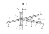
以下、図2を用いて、反射光での損失増加について詳細を説明する。図2は従来構造の光システムを示す図である。基本構造は図1のものと同様である。光導波路、1及び2を交差させ、その交差部に光学フィルタ4を設けている。本構造は、2θの角度で交差する2つの光導波路1と2の光軸の交点3が光学フィルタ4の等価的な反射中心面5上に合うように設計する必要がある。尚、図2において、光導波路1、2、および3の中心軸が各々符号6、7、及び8として示されている。
【0025】
今、光導波路の入射・反射角をθとする。光学フィルタ4がその法線方向にa移動すると、反射光の光軸は反射側の光導波路の軸7から2|a|sinθだけずれて7′となる。位置5は正しく設置された場合の光学フィルタの位置、位置5′はずれて設置された場合の光学フィルタの位置である。その結果、反射光は、光学フィルタの位置ずれに相当する光導波路30の一部を伝搬し、この為、反射側の位置7′にある光導波路31とうまく結合しない。従って、反射光は、散乱されて大きな損失が生じる。
【0026】
光学フィルタの位置ずれに対する反射光の損失増加の計算例を図3に示す。横軸がフィルタの所定位置からのずれ、縦軸は損失の増加分を示している。この結果によれば、光学フィルタ位置ずれのトレランスは、例えば0.2 dBの損失増加に抑えるには±2μmと非常に小さいことがわかる。
【0027】
ところが、光学フィルタの設置には溝入れもしくは切断等の機械的加工を用いる為に、加工精度の向上が困難で、光導波路径に比べて光学フィルタの作製誤差は無視できない程の大きさとなるのが実状である。この実際上の困難性が低損失な光合分波器の製造歩留りを低下させる要因となっている。そこで、光学フィルタ付光導波路を用いた光合分波器の製造歩留りの向上には、フィルタ位置ずれのトレランスを増加させるような光合分波器の構造が求められるのである。
【0028】
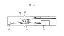
次に、光のクロストークの問題について言及する。図4はこうした例を示す光送受信モジュールの平面配置図である。図1に示した光合分波器16にフォトダイオード50とレーザーダイオード(LD)51を設置した構成を有する。光学フィルタ15は送信信号が有する波長の光を反射し、送信信号波長よりも長い受信信号が有する波長の光を透過するものを用いている。光送受信モジュールとする場合、LD等送信部で発生した漏れ光9が受信信号に影響を及ぼす光クロストークという問題が生じる。
【0029】
LD 51で発生した光は全てが導波路を伝播するわけではなく、LD−導波路結合損失が生じてLDが出す光のうち一部は導波路と結合せすに導波路の外に散乱される。またLD−光合分波器間の曲がり導波路においても導波光の一部が放射光19として導波路外を伝播する。これらが漏れ光9となるが、その多くは光学フィルタ15に達し、また光学フィルタへの入射角度はθとは異なる。
【0030】
図5に光学フィルタの透過特性の例を、その入射角度θが0の場合と、0より大きい場合を例示した。図5の特性において、透過損失の大きい領域が、反射に用いられる領域に対応する。一般に光学フィルタは、図5の例に見られるように、入射光の入射角度が異なると反射帯域が変化しまたアイソレーションも劣化する。前記図4の例では、本来導波路を導波する光を反射させる為に入射角θの光を反射するように設計した光学フィルタを用いる。従って、前記漏れ光の多くは入射角が前記のフィルタへの入射角θと異なる為に、これらの漏れ光の内、光学フィルタで遮断されずに透過する光も発生する。この透過した漏れ光がPD50に届くと、本来の受光信号にとっての雑音となって受信特性を劣化させる。
【0031】
この対策としてフィルタへの入射角θを0度に近づけることが考えられる。この対策は、フィルタの位置ずれによる反射光の光軸と導波路軸のずれも0に近いと、それに基づく損失増加は低減できる。また、逆に、漏れ光の入射角がθ程度となりフィルタで遮断できる。
【0032】
しかし、この対策を図1の光合分波器に適用すると、反射光が入射側の光導波路に戻るやすくなるという、いわゆる反射戻り光の問題が新たに生じる。図6はこの問題を示す説明図である。 前記の対策の実施は、2つの光導波路1と2が重なる部分17を増加させる。この為、入射角θの低減には限界がある。従って、入射角の低減の方策は、有効な実際的な解決策とはなり得なかった。
【0033】
本願発明はこうした諸問題を解決する。、前述したように、本願発明のマルチモード干渉型光導波路は、入射側の光導波路より入射光があった場合、出射側の光導波路の入り口近傍の光の強度分布の山となる為、前記入射光に対してほとんど損失を生じない。
【0034】
また、マルチモード干渉型光導波路に並置して設けられる入射側、及び反射光を射出側に導波する光導波路は、所定の個別位置に設置されるので、透過すべき光のフィルタでの反射戻り光が、射出側に導波する光導波路に混入し雑音となる問題は避けることが出来る。
【0035】
更に、後述するように、光学フィルタが、マルチモード干渉型光導波路に並置して設けられる光導波路を導波する入射角が0度に近い光信号を反射するようになされるので、本構造において、更に漏れ光として発生する光の入射角は、透過を許さない角度となり、漏れ光のフィルタを通しての透過は阻止される。
【0036】
以下に本願発明の主な発明の形態を列挙する。
【0037】
光学フィルタを有する本願発明の諸形態
本願の第1の形態は、第1、第2、及び第3の光導波路と、マルチモードでの光の伝搬が可能な第4の光導波路と、前記第4の光導波路内の光の進行方向に交差して設けられた光学フィルタとを少なくとも有し、前記第4の光導波路の第1の端面に前記第1の光導波路が接続され、前記第4の光導波路の第2の端面の所定の個別位置に前記第2及び第3の各光導波路が接続され、前記第4の光導波路は、前記第2および第3の光導波路のいずれかの光導波路からの第1の波長の光入力が前記第4の光導波路内の光の伝搬によって、前記第1の光導波路内に前記第1の波長の光入力に対応する光の伝搬を可能となし、且つ前記第2および第3の光導波路のいずれかの光導波路からの第2の波長の光入力が前記光学フィルタでの反射を介して、前記第2および第3の光導波路の内の光入力のない光導波路内に前記第2の波長の光入力に対応する光の伝搬を可能となすマルチモードでの光の伝搬が可能である光導波路であることを特徴とする光導波路を有する光システムである。
【0038】
前記第1、第2、及び第3の各光導波路は、シングルモード、あるいはマルチモードでの光の伝播が可能な光導波路を用いることが出来る。光多重通信においては、多くはシングルモードの光を用いており、本願発明はこの目的に供してわけても有用である。
【0039】
しかし、マルチモードの光を用いる場合においても、本願発明を用いることによって、好都合な光合分波器機能を実現することが出来る。それは、本願発明に係るマルチモード干渉型光導波路が、マルチモードあるいはシングルモードでの光に対して同様の機能を果たすからである。このマルチモード干渉型光導波路の機能は、本願発明の基本的事項であり、以下、特にことわらない場合においても、本願明細書に示される発明の諸形態に考慮されることである。
【0040】
従って、この形態を本願の第2の形態として例示すれば、それは、シングルモードでの光の伝搬が可能な第1、第2、及び第3の光導波路と、マルチモードでの光の伝搬が可能な第4の光導波路と、前記第4の光導波路内の光の進行方向に交差して設けられた光学フィルタとを少なくとも有し、前記第1の光導波路が前記第4の光導波路の第1の端面に接続され、前記第2及び第3の各光導波路が前記第4の光導波路の前記第1の端面に対向する第2の端面の所定の個別位置に接続され、前記第4の光導波路の第1の端面および第2の端面は各々当該第4の光導波路内の光の進行方向と交差する端面であり、前記第4の光導波路は、前記第2および第3の光導波路のいずれかの光導波路からの第1の波長の光入力が前記第4の光導波路内の光の伝搬によって、前記光学フィルタを透過した上で前記第1の光導波路内に前記第1の波長の光入力に対応するシングルモードでの光の伝搬を可能となし、且つ前記第2および第3の光導波路のいずれかの光導波路からの第2の波長の光入力が前記光学フィルタでの反射を介して、前記第2および第3の光導波路の内の光入力のない光導波路内に前記第2の波長の光入力に対応するシングルモードでの光の伝搬を可能となす、マルチモードでの光の伝搬が可能な光導波路である光導波路を有する光システムである。
【0041】
本願発明の第4の形態は、第1、第2、及び第3の光導波路と、マルチモードでの光の伝搬が可能な第4の光導波路と、前記第4の光導波路内の光の進行方向に交差して設けられた光学フィルタと、を少なくとも有し、前記第1の光導波路が前記第4の光導波路の第1の端面に接続され、前記第2及び第3の各光導波路が前記第4の光導波路の前記第1の端面に対向する第2の端面の所定の個別位置に接続され、前記第4の光導波路は、前記第1及び第2の端面から所定距離離れた2つの平面における光強度分布の規格化された各形状を重ねた場合、前記各形状が相互に前記第4の光導波路の光の進行方向に沿う中心軸に対して線対称ないしは略線対称となっている光導波路である光導波路を有する光システムである。
【0042】
本願発明の第5の形態は、第1の光導波路が、マルチモードでの光の伝搬が可能な第4の光導波路の第1の端面に接続され、前記第4の光導波路の前記第1の端面に対向する第2の端面に第2、及び第3の光導波路がその接続位置において所定間隔で接続され、前記第4の光導波路内に光学フィルタが設置され、前記光学フィルタの入射面は、前記第1、第2、および第3の各光導波路の前記第4の光導波路への接続位置における当該第1、第2、および第3の各光導波路での光の波面と平行ないしは略平行であることを特徴とする光導波路を有する光システムである。
【0043】
ここで、本願発明のマルチモード干渉型光導波路が、入射側の光導波路より入射光があった場合、出射側の光導波路の入り口近傍の光の強度分布の山となす構成について補足説明する。このことによって、合わせて、マルチモード干渉型光導波路に並置して設けられる入射側、及び反射光を射出側に導波する光導波路は、所定の個別位置に設置されること、そして、このことによって、透過すべき光のフィルタでの反射戻り光が、射出側に導波する光導波路に混入し雑音となる問題は避けることが出来る旨が十分理解できるであろう。
【0044】
マルチモード干渉型光導波路における光の伝搬の状態を示す図7を参酌する。
【0045】
ここで、信号光の波長をλ、 マルチモード干渉型光導波路の屈折率をnとする。前記 マルチモード干渉型光導波路の長さL、幅W、及び接合部に設けられる光導波路の中心軸とマルチモード干渉型光導波路の中心軸よりの位置Dとの関係は次の式によって与えられる。尚、前記各光導波路の中心軸は光の進行方向に沿った中心軸である。
【0046】
L=α(4nW2)/3λ 式(1)
D=βW/6 式(2)
αおよびβは補正係数である。
【0047】
これらの関係を満たすことで、第1の光導波路11の入り口近傍が光の強度分布の山となり、光導波路12からの入射光に対してほとんど損失を生じずに再び光導波路11を導波させることが出来る。光学フィルタ15よりの反射に関しても鏡像を考えれば前記の光導波路11の場合と全く同様である。
【0048】
即ち、透過光(λ1)と反射光(λ2)に対する光の進行方向に沿うマルチモード干渉型光導波路の距離を、各々L及びL′とすれば、
L: L′=1/λ1:1/λ2 式(3)
の関係にある。
【0049】
更に、
L =α(4nW2)/3λ1 式(4)
L′=α(4nW2)/3λ2 式(5)
の関係にあることは容易に理解されるであろう。
【0050】
尚、この場合、光導波路のコア、クラッドの具体的材料、具体的構造の理論よりのずれ等によって理論的な関係を補正する必要が生ずる。前記αおよびβがこの補正係数である。この補正係数αおよびβは、通例、いずれも概ね、1.5倍以内である。しかし、いずれにしても前記式(1)、式(2)を満足する光導波路を実現することが出来る。尚、ここで、前記マルチモード光導波路の実際的な長さLが1.5mmないし2.0mmの範囲、実際的な幅Wが30μmないし40μmの範囲が多用される。更には、マルチモード干渉型光導波路の実際的な長さLが1mmないし5mmの範囲、実際的な幅Wが25μmないし70μmの範囲から選択されることがより実際的であり、好ましいことは前述した通りである。
【0051】
尚、このマルチモード干渉自体の理論は、例えばJOURNAL OF LIGHTWAVE TECHNOLOHGY、 Vol.13、NO.4、APRIL1995、pp.615−627を参酌することが出来る。本願発明はこの理論を用いて光システムを構築したことにある。
【0052】
本願の第6の形態は、平面基板上に形成された複数の波長を有する信号光を合波または分波する光合分波器において、マルチモード干渉型光導波路と、前記マルチモード干渉型光導波路の片側に接続した第1の光導波路と、前記マルチモード干渉型光導波路の前記第1の光導波路と反対側に接続した第2及び第3の光導波路と、前記マルチモード干渉型光導波路内に設置される光学フィルタで構成され、前記第2及び第3の光導波路が前記マルチモード干渉型光導波路との結合部において所定の間隔を有することを特徴とする、光合分波器である。
【0053】
本願の第7の形態は、本願発明の光合分波器もしくは光導波路素子において、光学フィルタがマルチモード干渉型光導波路を導波するマルチモード光の進行方向(通称、光軸)に対して垂直あるいは略垂直に設置されている形態である。
【0054】
本願発明においては、マルチモード干渉型光導波路の一方の端面に複数の光導波路、例えば、図7の光導波路12および13、が所定の個別位置に設置されている。従って、光学フィルタがマルチモード干渉型光導波路を導波するマルチモード光の進行方向に対して垂直あるいは略垂直に設置されている為、一方の光導波路、例えば、前記光導波路13から入射された光が前記光学フィルタに達しても、不必要な漏れ光として雑音を構成することはない。
【0055】
本願発明は、マルチモード干渉型光導波路に接続する複数の光導波路において、少なくとも前記第1から第3のうちいずれか1つ以上の光導波路から入射した信号光が、それぞれ前記マルチモード干渉型光導波路でマルチモード光として伝播した後、所定の波長を有する信号光が前記第1から第3のうちいずれか1つ以上の光導波路と結合するように、前記マルチモード干渉型光導波路の長さ及び幅と、前記マルチモード干渉型光導波路と前記第1から第3の光導波路の接続部が調整されていると言うことが出来る。
【0056】
本願の別な形態によれば、前記第2及び第3の光導波路の光軸、例えば、図7の光導波路12および13における光軸の延長線が前記マルチモード干渉型光導波路の外に交点を持つ、もしくは互いに平行あるいは略平行であることが、実用上、極めて好都合である。こうして、一方の光導波路、例えば、前記光導波路13から入射された光が前記光学フィルタに達しても、不必要な漏れ光として雑音を構成することはない。更に、各光導波路は任意の方向に曲げて用いることが出来る。これにより、各光導波路を漏れ光の分布する領域から反して、雑音の発生を抑制することが可能である。この利点は、より大きな光システムの構築の設計を容易にする。
【0057】
本願発明の別な形態によれば、前記第4の光導波路が前記マルチモード干渉型導波路と前記第1の光導波路側で接続する、もしくは前記第1から第4の光導波路以外に複数の光導波路が前記マルチモード干渉型導波路と接続するなど、具体的な用途の目的に応じて種々応用形態を考えることが出来る。
【0058】
更に、本願発明の別な形態によれば、前記第1から第4の光導波路の全てもしくは一部の端面に、それぞれ発光素子もしくは受光素子もしくは光ファイバもしくは光ファイバとの接続手段を設けることが出来る。こうして、所望の光送信モジュールもしくは光受信モジュール、光送受信モジュールもしくは光合分波モジュールを得ることが出来る。こうした、光受信モジュール、光送受信モジュールもしくは光合分波モジュールの具体例は後述される。又、こうした発光素子や受光素子は、前記第1から第4の各光導波路に代えて、直接マルチモード干渉型導波路に接続することが出来る。この方法は介在する光導波路による光の吸収を避ける点で好ましい。勿論、マルチモード干渉型導波路と、別異の光導波路を介してこれらの発光、受光素子とを接続することが出来る。
【0059】
本例の代表的な例を示せば、それは、第1、第2、及び第3の光導波路と、マルチモードでの光の伝搬が可能な第4の光導波路と、前記第4の光導波路内の光の進行方向に交差して設けられた光学フィルタとを少なくとも有し、前記第1の光導波路が前記第4の光導波路の第1の端面に接続され、前記第2及び第3の各光導波路が前記第4の光導波路の前記第1の端面に対向する第2の端面の所定の個別位置に接続され、前記第4の光導波路の第1の端面および第2の端面は各々当該第4の光導波路内の光の進行方向と交差する端面であり、前記第4の光導波路は、前記第2および第3の光導波路のいずれかの光導波路からの第1の波長の光入力が前記第4の光導波路内の光の伝搬によって、前記光学フィルタを透過した上で前記第1の光導波路内に前記第1の波長の光入力に対応する光の伝搬を可能となし、且つ前記第2および第3の光導波路のいずれかの光導波路からの第2の波長の光入力が前記光学フィルタでの反射を介して、前記第2および第3の光導波路の内の光入力のない光導波路内に前記第2の波長の光入力に対応する光の伝搬を可能となす、マルチモードでの光の伝搬が可能な光導波路であり、且つ前記第1より第3の光導波路の少なくとも一つに接続する発光部あるいは受光部の設置した、あるいは前記第1より第3の光導波路の少なくとも一つに代えて発光部あるいは受光部を設置したことを特徴とする光導波路を有する光システムであると言うことが出来る。
【0060】
こうした光合分波器もしくは光導波路素子を用いた光送受信モジュールの場合にも、次の構成によって、漏れ光の遮断を行うことが出来る。即ち、前記送信手段で作られ送信信号の一部で前記送信手段と接続した光導波路の外部を伝播する漏れ光の波面が前記光学フィルタの作る平面と平行あるいは略平行であることにより、前記漏れ光が遮断される。
【0061】
従って、このような例の代表な形態は、光合分波器もしくは光導波路素子と、前記第1もしくは第4の光導波路の両方もしくは片方の端面に受光手段として設けた受光素子もしくは光ファイバもしくは光ファイバの接続手段と、前記第2もしくは第3の光導波路の両方もしくは片方の端面に送信手段として設けた発光素子もしくは光ファイバもしくは光ファイバとの接続手段で構成され、前記送信手段で作られ送信信号の一部で前記送信手段と接続した光導波路の外部を伝播する漏れ光の波面が前記光学フィルタの作る平面と平行あるいは略平行であることにより、前記漏れ光が遮断されることを特徴とする光送受信モジュールであると言うことが出来る。
【0062】
更に、本願発明の別な形態によれば、次のような光送信モジュール、光受信モジュール、光送受信モジュールもしくは光合分波モジュールを実現することが出来る。即ち、これらの光送信モジュール、光受信モジュール、光送受信モジュールもしくは光合分波モジュールに、前記漏れ光を遮断する為に、前記光学フィルタ以外に1個以上の光学フィルタを設ける、もしくは前記第1から第4の光導波路及び前記複数の導波路以外に1個以上の導波路もしくは導波路層もしくはクラッドと屈折率の異なる部材を設けることがより有用である。
【0063】
更に、本願発明の係る諸光合分波器もしくは諸光導波路素子に、発光素子もしくは受光素子もしくは光スイッチもしくは光学フィルタもしくは光増幅器もしくは光変調器等の光素子を組み合わせて用いることが出来る。
【0064】
更には、本願発明に係る諸光合分波器もしくは諸光導波路素子を複数用いて、発光素子もしくは受光素子もしくは光スイッチもしくは光学フィルタもしくは光増幅器もしくは光変調器等の複数の光素子と組み合わせ、複数の信号を同時に処理するもしくは複数の波長を有する信号光を多段階で処理することが可能である。
【0065】
更には、本願発明に係る諸光モジュールに、集積回路もしくはプリアンプ等の電気信号処理手段を組み合わせ光通信モジュール、あるいは光通信装置に供することが出来る。
【0066】
光学フィルタを有さない本願発明の諸形態
次に、本願の別な形態として、これまで説明してきた光導波路を有する光システムにおいて、前記光学フィルタを設置する前の構成体も重要な形態である。勿論、光導波路を有する光システムを光合分波器あるいは光送信モジュール、光受信モジュール、光送受信モジュールとして用いる為には、所定の特性の光学フィルタを設置する必要があることは言うまでもない。しかし、本願に係る光導波路を有する光システムを、実際に用いるに当っては、頭初、光学フィルタを設けない形態でまず、準備し、それから光学フィルタを挿入設置することも実際的である。図20は、基板20に光学フィルタ15が設置された状態をしめす拡大断面図である。図20の例は、基板20上に第1及び第2のクラッド層21、23が形成され、フィルタ挿入用の溝24が設けられている。フィルタ15は接着層95で固定される。尚、この断面図はコア領域を含まない部分の断面図である。
【0067】
従って、本形態の代表的な形態は、第1、第2、及び第3の光導波路と、マルチモードでの光の伝搬が可能な第4の光導波路と、前記第4の光導波路内に光学フィルタを当該第4の光導波路内の光の進行方向に交差して設置する為の手段とを少なくとも有し、前記第4の光導波路の第1の端面に前記第1の光導波路が接続され、前記第4の光導波路の第2の端面の所定の個別位置に前記第2及び第3の各光導波路が接続され、前記第4の光導波路は、前記第2および第3の光導波路のいずれかの光導波路からの第1の波長の光入力が前記第4の光導波路内の光の伝搬によって、前記第1の光導波路内に前記第1の波長の光入力に対応する光の伝搬を可能となし、且つ前記第2および第3の光導波路のいずれかの光導波路からの第2の波長の光入力が前記光学フィルタでの反射を介して、前記第2および第3の光導波路の内の光入力のない光導波路内に前記第2の波長の光入力に対応する光の伝搬を可能となすマルチモードでの光の伝搬が可能である光導波路であることを特徴とする光導波路を有する光システムであると言うことが出来る。
【0068】
本願のこの光学フィルタを設置する以前の諸形態は、光学フィルタを設置した前記した全ての諸形態に考えることが可能である。従って、更なる説明および諸形態の列挙は省略する。
【0069】
発明の実施の諸形態
次に、本願発明の具体的な実施の諸形態する。
【0070】
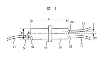
図8は本発明の第1の実施例である光合分波器の実施形態を示す斜視図である。図9はその合分波部の拡大平面図である。
【0071】
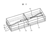
所定の基板、例えばシリコン(Si)基板20上に、屈折率の異なる2種類のフッ素化ポリイミド樹脂を用いて光導波路を形成する。この光導波路は、少なくとも、第1のクラッド層21、コア領域22、そして第2のクラッド層23を有して構成される。ここで、24はフィルタ挿入用の溝である。このとき、各層の厚さの例を示せば、下部クラッド層21の厚さは5μm、コア22の厚さは6.5μm、上部クラッド層23の厚さは15μmである。コアとクラッドとの屈折率比は0.3%とした。合分波部は、少なくともマルチモード干渉型導波路10と第1の光導波路11、第2の光導波路12、及び第3の光導波路13を有する。マルチモード干渉型導波路の幅Wは25μm、長さLは1200μm、光導波路の間隔Dは5μmである。又、3つの光導波路の幅は6.5μmとした。
【0072】
光学フィルタ15は入射角0度の光に対して波長1.3μmの光を反射し、且つ波長1.5μmの光を透過する誘電体多層膜フィルタ15が用いられた。その厚さは15μmである。この誘電体多層膜フィルタ自体を通例のものを用いて十分である。そして、マルチモード干渉型導波路の中央部に、幅15μmの溝24に挿入し、UV(Ultra―Violet)硬化材95を用いて固定した。この溝24は、例えばダイシングソーによって形成することが出来る。第2及び第3の光導波路12、13はマルチモード干渉型導波路との接続部32及び33において互いに平行あるいは略平行となっている。
【0073】
図19に光学フィルタ15が基板20に装着された状態の断面図を示す。符号24はこの反射手段を設置する為の溝である。符号21、23は各々当該光導波路のクラッド層を示している。反射手段15の固定には接着剤95が用いられた。
【0074】
尚、図10、図14、及び図15に図8と類似の光導波路の構成が示される。そして、この構造は図8と類似の積層構造を有する。しかし、こうした光導波路の構成自体は通例のもので十分である。従って、以下の図面は、個別の積層を詳細な図示を省略する。
【0075】
第2及び第3の光導波路12、13が接続部32、33で平行となることによって、マルチモード干渉型導波路内に励起されたマルチモード光の光軸が前記光学フィルタに対して垂直となる。その結果、フィルタ15に位置ずれが生じても、このフィルタ15の反射光の光軸と導波路軸のずれは全く生じない。
【0076】
ここで、前記光学フィルタは誘電体多層膜フィルタとは限らず、例えばダイシング溝24等の光学フィルタ設置手段のみを備えた図10のような光導波路素子であってもよい。図10では他の部材は図8と同様なので、詳細説明は省略する。
【0077】
本願発明の係る光導波路を有する光システムは、光合分波器への入力する複数の光導波路、及び光合分波器より出力される複数の光導波路をそれぞれ有する形態も取ることが出来る。上記複数の光導波路がいずれもシングル・モードの光導波路、又、光合分波器がマルチモード干渉型光導波路を有する光合分波器であることは言うまでもない。
【0078】
図11はこうした一例を示す光合分波器部分の平面図である。この例はマルチモード干渉型導波路10の入射側に複数、具体的には2つの光導波路12、13が設けられている。一方、マルチモード干渉型導波路10の出射側に複数、具体的には2つの光導波路11、14が設けられている。図11は第4の光導波路14が符号34の位置に設けられている外は、図9と同等であるので、同じ部位、部材は同じ符号を用いている。
【0079】
もちろん、さらに複数の光導波路がマルチモード干渉型導波路と接続して、複数の光合分波器であってもよいことは言うまでもない。
【0080】
本願発明に係わる構造と図1に示す従来構造の光合分波器について、フィルタ部に関する製造トレランスを比較した。
【0081】
図12はフィルタの位置ずれによる反射光の損失増加量を示す。横軸はフィルタの位置ずれの距離、縦軸は反射光の損失増加量の例を示す。曲線35は本実施例の場合また曲線36は従来構造の場合の特性を表す。設計上許容される損失として例えば0.2dB程度とすると、トレランスは従来構造が1μmであるのに対し本実施例では10μm程度となる。このように、従来構造に比較して、充分大きな製造トレランスを実現することが出来る。
【0082】
更に、ここで、本例におけるフィルタの位置ずれに対する損失増加は、反射光の光軸と導波路軸のずれによるのではなく、マルチモード干渉型導波路内でのマルチモード光の干渉による強度分布に起因することを指摘しておかなければならない。
【0083】
図13は、マルチモード干渉型導波路の長さLを変化させたときの強度(損失)変化を示す。横軸はマルチモード干渉型導波路の長さL、縦軸は損失を示している。ここで、曲線37と曲線38はそれぞれ図7において第2の光導波路12から入射させたシングルモード光の第1の光導波路11及び第4の光導波路14とマルチモード干渉型導波路10との接合部31及び34における損失量を表す。両者の強度のピークが2400μm程度で周期的に現れることがわかる。
【0084】
従って、前述の図12をもって示したフィルタの位置ずれに対する損失増加に対して、図13に例示したマルチモード干渉型導波路内でのマルチモード光の干渉による強度分布に起因する損失が含まれることとなる。その損失の周期によって、フィルタの位置ずれに対する損失増加に対する、マルチモード光の干渉による強度分布に起因する損失の割合が高くなる。わけても、本願発明の例では、反射光に基づく損失が基本的になく、フィルタの位置ずれに対する損失増加は、このマルチモード光の干渉による強度分布に起因する損失によるものである。
【0085】
次に、波長多重通信への、本願発明の光導波路を有する光システムの適用例を例示する。
【0086】
図14は本発明の第2の実施例である光合分波モジュールの実施形態を示す斜視図である。第1の実施例として例示した光合分波器に対して、その3つの光導波路の端面に光ファイバを設置するためのV溝41、42、43を形成した。このV溝41、42、43は、シリコン基板20に、通例の結晶面に対する異方性食刻の技術を用いて容易に形成することが出来る。そして、この溝は光ファイバの位置設定に極めて実用的である。
【0087】
本実施例は、例えば、次のように用いることが出来る。例えば、光学フィルタ15として、波長1.3μmの光を透過し波長1.5μmの光を反射する光学フィルタを用いた場合を検討する。光ファイバ46から波長1.3μmと1.5μmの波長多重光を入射する。この波長多重光は、光学フィルタ15で波長1.3μm の光が透過され、一方1.5μmの光は反射される。従って、波長1.3μm の光は光ファイバ44に入射する。他方、1.5μmの反射光は光ファイバ45に入射する。こうして、一つの波長多重光から、1.3μmもしくは1.5μmの各波長を有する信号光をそれぞれ光ファイバ44と45に分波することがと出来る。
【0088】
また、出入射を逆転すれば合波器としても機能することは言うまでもない。
【0089】
尚、光ファイバ接続はV溝に限らず、導波路基板に接続用の台を設けて光ファイバと接着剤により接着する等他の手段によるものであってもよい。
【0090】
図15は本発明の第3の実施例である光送受信モジュールの実施形態を示す斜視図である。即ち、本例は、本願の光導波路を有する光システムが、光の発光素子及び受光素子を一つの基板に搭載して設けた例を示す。この例は光の送受信器の実際的な形態として用い易く有用である。
【0091】
第1の実施例として例示した光合分波器のシリコン基板20に、受光素子であるフォトダイオード51及び発光素子であるレーザーダイオード52を設置した。即ち、シリコン基板20上にこれまでの例と同様に、光導波路の為のポリマーの多層膜を形成する。そして、その所定部分のポリマを除去してSi基板20を露出させる。このポリマーの除去は通例のドライエッチングを用いて十分である。このシリコン基板上の所定位置に当該発光、受光素子の各々の第1の電極、52、及び53を形成する。そして、第1の光導波路の端面にフォトダイオード51を搭載し、第3の光導波路の端面にレーザーダイオード52を搭載した。前記電極と発光、受光の各素子の相互の間は半田によって接続した。尚、図において、発光、受光の各素子の各第2の電極は省略されている。その他の構成は前記の第1の実施例と同様である。従って、同一部分、部材は同一符号をもって示されている。
【0092】
図16は、本発明の第4の実施例である光送受信モジュールの実施形態を示す斜視図である。本例は前記第3の実施例において、フォトダイオード51及び53をマルチモード導波路10に関して光導波路12側へ移動させ、更に光導波路11の曲がり方向を変更した例を示す。本変更によりレーザダイオード52で発生した光のうち光導波路13と結合出来なかった漏れ光の分布中心から、受信部が離れることにより漏れ光の影響を小さくすることが出来る。
【0093】
尚、フォトダイオード及びレーザーダイオードの設置の方法は本実施例の組み合わせは限定されない。勿論、発光、受光の各素子のいずれか一方だけを、前記シリコン基板に搭載した形態も、勿論目的によって用いることが出来ることは言うまでもない。更に、必要に応じて、3個以上の発光、受光の各素子を搭載した形態も取り得ることは言うまでもない。
【0094】
次に、本願の光導波路を有する光システムが、光増幅器に用いられた例を示す。
【0095】
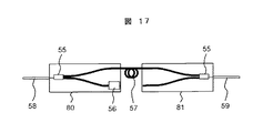
図17は本発明の第4の実施例である光増幅器の実施形態を示す平面構成図である。2つのSi基板、80、81上に光合分波器55を1つずつ形成した。そして、片方のシリコン基板80にはポンプ用レーザーダイオード56を設置した。尚、前記光合分波器55は、例えば前記実施例1に示した構成を用いて十分である。また2つの基板間は、例えば長さ1m程度のエルビウムドープファイバ(一般にファイバ増幅器とも称する)57でつないだ。
【0096】
光ファイバ58から入射した光は、波長の異なるレーザーダイオード56からの光と合波し、エルビウムドープファイバ57で増幅される。そして、この増幅された光は、再び、異なる波長成分に分波され、所望波長の光が光ファイバ59より出射する。こうして、ファイバー58より入射した光が増幅され、増幅された所望の波長の光を、ファイバ59より得ることが出来る。
【0097】
更に、本願の光導波路を有する光システムが、光受信モジュールに用いられた例を示す。
【0098】
図18は本発明の第5の実施例である光受信モジュールの実施形態を示す基本的な平面構成図である。本例は、本願発明を光受信モジュールに適用した例である。この光受信モジュールは、波長多重信号光を各波長毎に分波し、これらをおのおのその波長に適した受光素子で受光するものである。
【0099】
本例の基本構成は次の通りである。光ファイバー65からの光信号を2つのフィルタ63、64によって所望の波長に光を選択する。そして、この選択された波長の光は、そのフィルタの透過側に設けられた光受光素子62−1、62−2、62−3、62−4、62−5、62−6によって検知される。
【0100】
図18を参酌すれば、これまでの諸例と同様に、Si基板上に光合分波器60とそれらを結ぶ光導波路61を複数形成する。そして、各合分波器の透過側端面に複数のフォトダイオード62−1、62−2、62−3、62−4、62−5、62−6を配置した。光導波路61の一方の端面、即ち入射光導波路は光導波路65に接続され、この光導波路65、例えば光ファイバーは当該光受信モジュールへの光入力を導波する。前記光合分波器60は、例えば前記実施例1に示した構造を用いて十分である。この例では、マルチモード干渉型光導波路90に一方の端面に直接受光素子62−1が設けられている例である。マルチモード干渉型光導波路90とこの内部に設けた光学フィルタ63、マルチモード干渉型光導波路90の一方の端面に配置された光導波路91、92によって本願発明に係わる光システムの基本形態が構成される。従って、図17に示された例は、6つの本願発明に係わる光システムが縦に接続された形態である。尚、図17では、説明の都合上、光導波路91、92のみ個別の符号を付し、その他は符号61を付したが基本的に同様の光導波路である。
【0101】
尚、光学フィルタ63、おるいは64は複数の光システムに共通する物理的形態をもって構成されている。しかし、光学フィルタ63、64は位置によって反射・透過の波長特性が変化するものを用いる。この光学フィルタ63、64は、その光合分波器60に対応する位置の反射・透過特性が当該光システムでの所望の波長を透過するように設計されている。反射・透過特性が変化する光学フィルタの具体的な例はフィルタの入射、透過の面を構成する2つの面の間隔を変化させたものである。あるいは、所定の位置のフィルタ材料を別異の材料を用いることも可能である。尚、本例では、透過・反射特性が場所によって変化する光学フィルタを2枚用いるが、これら所望場所に対応する各特性を有する光フィルタを複数個用いることも当然可能である。この場合、光学フィルタの特性はその厚さを変化させることによっても達成することが出来る。
【0102】
本モジュールは、光ファイバから入射した波長多重信号光を各合分波器で1波長ずつ順に分波し、各フォトダイオードで受光することができる。
【0103】
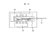
第6の実施例は、本願発明の光の送受信が可能な光通信モジュールへの適用例である。
【0104】
図19は本発明の第6の実施例である光通信モジュールの概略を示す平面配置図である。尚、図は主要部材の基本配置を示す。光送受信モジュール66には前記第3の実施例に示した構造を用いた。本光通信モジュールは、送信用IC67や受信用IC68、また温度を制御する為のペルチェ素子69を組み合わせて用いられた。本モジュールにより、光ファイバ70より受信した光信号をデジタル電気信号に変換し、また反対に生成した電気信号を同じ光ファイバより光信号として送信することができる。本実施例は送信用と受信用のICを別体としたが、一体としてもよいし逆に増幅器やAPC等を分けて設置してもよいことは言うまでもない。
【0105】
本発明の実施例は特に、Si基板上にフッ素化ポリイミドを用いて合分波器もしくは合分波器を含むモジュールを作製することについて述べたが、当然のことながら、基板はSiではなく石英等他の材料であってもよいし、光導波路はフッ素化ポリイミドではなく他のポリマーや石英等の材料であってもよいことは言うまでもない。
【0106】
本発明の実施例は特に、波長1.3μmの光を透過し波長1.5μmの光を反射する光学フィルタを用いた合分波器もしくは合分波器を含むモジュールを作製することについて述べたが、光学フィルタは波長特性の異なるものでもよく、その場合他の波長を有する波長多重光を合分波することも可能であることは言うまでもない。
【0107】
以上、本願発明を詳細に説明したが、本発明はマルチモード干渉型導波路を反射構造に用いた光合分波器もしくはそれらを用いた光送受信モジュールに関するものであり、光合分波器の入射・反射導波路はマルチモード干渉型導波路との接続部において平行であることを特徴としている。
【0108】
その結果、フィルタの位置ずれによる損失増加はマルチモード干渉型導波路における干渉の周期のみに起因し、フィルタ部の製造トレランスが大きくなる。従って歩留りが向上しコストを低減できる。また、反射角0度のフィルタを使用できることから漏れ光が充分に遮断され、光クロストークの問題が解決される。従って受光素子の受信感度等の損失設計に余裕が生まれる。
【0109】
【発明の効果】
本願発明によれば、安価に光導波路を有する光システムに十分安定した光伝達特性を与えることが出来る。
【0110】
本願発明によれば、製造歩留の高い光導波路を有する光システムを提供することが出来る。
【0111】
本願発明は、マルチモード干渉型光導波路の相対する端面に設けた光導波路相互での光の漏れ光を防止することが出来る。
【図面の簡単な説明】
【図1】図1は従来の技術による光合波器部分の概略平面図である。
【図2】図2は光学フィルタのずれた状態を説明する光合波器部分の概略平面図である。
【図3】図3は従来構造における、光学フィルタの位置ずれと反射光の損失増加の関係を示す図である。
【図4】図4は従来構成になる別な光システムを示す概略平面図である。
【図5】図5は入射角の異なる光に対する光学フィルタの透過特性を示す図である。
【図6】図6は従来構造の光合分波器におけるθを0度に近づけたときの構造を示す平面図である。
【図7】図7は本願発明の光合分波器部分のマルチモード干渉を模式的に示す平面図である。
【図8】図8は本願発明の第1の実施例である光合分波器部分を示す斜視図である。
【図9】図9は本願発明の第1の実施例である光合分波器部分の平面拡大図である。
【図10】図10は光学フィルタを設置する前の光システムの斜視図である。
【図11】図11は光学フィルタを設置する前の光システムの拡大平面図である。
【図12】図12は本願発明の第1の実施例と従来構造の光合分波器部分について、フィルタの位置ずれと反射光損失量の関係を示す図である。
【図13】図13はマルチモード干渉型導波路の長さと光強度の関係を示す図である。
【図14】図14は本願発明の第2の実施例である光合分波モジュールを示す斜視図である。
【図15】図15は本願発明の第3の実施例である光送受信モジュールを示す斜視図である。
【図16】図16は本願発明の第3の実施例である光送受信モジュールの別な例を示す斜視図である。
【図17】図17は本願発明の第4の実施例である光導波路モジュールを示す概略平面図である。
【図18】図18は本発明の第5の実施例である光受信モジュールを示す概略平面図である。
【図19】図18は本願発明の第6の実施例である光通信モジュールの各部材の配置を示す図である。
【図20】図20は光学フィルタの設置を説明する断面図である。
【符号の説明】
1:光導波路(入射側光導波路)、2:光導波路(反射側光導波路)、3:光導波路1及び2それぞれの光軸の交点、4:光学フィルタ、5:光学フィルタの等価的反射中心面、6:入射側光導波路の軸、7:反射側光導波路の軸、8:フィルタ位置がずれたときの反射光の光軸、9:漏れ光、10:マルチモード干渉型光導波路、11:第1の光導波路、12:第2の光導波路、13:第3の光導波路、14:第4の光導波路、15:光学フィルタ、16:従来構造の光合分波器、17:光導波路1及び2の重なり部分、18:反射戻り光、20:基板(例えば、Si基板)、21:下部クラッド層、22:コア層、23:上部クラッド層、24:マルチモード干渉型導波路と第1の光導波路の結合部、25:マルチモード干渉型導波路と第2の光導波路の結合部、26:マルチモード干渉型導波路と第3の光導波路の結合部、27:マルチモード干渉型導波路と第4の光導波路の結合部、28:本実施例におけるフィルタの位置ずれによる反射光の損失増加量、29:従来構造の光合分波器におけるフィルタの位置ずれによる反射光の損失増加量、30:第2の光導波路12からシングルモード光を入射した光の接合部31における損失、31:第2の光導波路12からシングルモード光を入射した光の接合部34における損失、32:光ファイバ設置用のV溝、33:光ファイバ設置用のV溝、34:光ファイバ設置用のV溝、35:フォトダイオード、36:レーザーダイオード、37:フォトダイオード用電極、38:レーザーダイオード用電極、39:第1の実施例である光合分波器、40:光合分波器間を結ぶ光導波路、41:複数のフォトダイオード、42:光学フィルタ、43:光学フィルタ、44:光ファイバ、45:光送受信モジュール、46:送信用IC、47:受信用IC、48:ペルチェ素子、49光ファイバ。[0001]
BACKGROUND OF THE INVENTION
The present invention relates to an optical system having an optical waveguide, and more particularly to an optical system having a so-called multi-mode interference (MMI) type optical waveguide. According to the present invention, an extremely good optical multiplexer / demultiplexer can be provided.
[0002]
[Prior art]
With the recent development of multimedia communication including the Internet, research on optical wavelength division multiplexing (WDM) technology for high-speed and large-capacity communication has become active. One of the optical components that is important in constructing a WDM communication system is an optical multiplexer / demultiplexer that multiplexes or demultiplexes light having a plurality of wavelengths. In particular, from the viewpoint of cost reduction, downsizing, and higher functionality, integration is achieved by forming an optical waveguide and optical multiplexer / demultiplexer made of quartz (glass) or polymer on a substrate and mounting an optical transceiver, etc. Attention has been focused on how to achieve this.
[0003]
As an optical multiplexer / demultiplexer, a filter type, a directional coupler type, a Mach-Zehnder interferometer type, or the like is known. Further, as a filter type that is advantageous for downsizing of a module, for example, a technique described in Japanese Patent Laid-Open No. 8-190026 (Article 1) is known.
[0004]
FIG. 1 shows the filter type optical multiplexer / demultiplexer shown in the
[0005]
[Problems to be solved by the invention]
The first problem to be solved by the present invention is that the reflection means, for example, typically an optical filter is installed in the multimode interference optical waveguide, and the reflection means is installed in an optical system using the reflection light. It is to reduce the tolerance for the deviation. That is, the change in the light transmission characteristics of the multimode interference optical waveguide based on the deviation of the installation position of the reflecting means is made as small as possible. When the reflected light from the reflecting means is used, the positional deviation of the reflecting means is an optical path that is at least twice the distance of the incident light to the reflecting means. For this reason, in order to ensure sufficient propagation characteristics, it is important to reduce the tolerance against the deviation of the installation position of the reflecting means.
[0006]
The second problem to be solved by the present invention is to prevent light leakage between the optical waveguides provided on the opposite end faces of the multimode interference optical waveguide.
[0007]
[Means for Solving the Problems]
A typical form for solving the first problem of the present invention can be used in, for example, an optical multiplexer / demultiplexer that multiplexes or demultiplexes signal light having a plurality of wavelengths formed on a flat substrate. According to the present invention, the first and second problems can be solved together.
[0008]
A representative form of the present invention includes first, second, and third optical waveguides, a fourth optical waveguide capable of propagating light in multimode, and the light in the fourth optical waveguide. An optical filter provided to intersect the traveling direction, the first optical waveguide is connected to a first end surface of the fourth optical waveguide, and the second and third optical waveguides are The fourth optical waveguide is connected to a predetermined individual position on the second end surface facing the first end surface, and the first end surface and the second end surface of the fourth optical waveguide are respectively connected to the fourth end surface. The fourth optical waveguide is an end face that intersects the traveling direction of light in the optical waveguide, and the fourth optical waveguide receives light of the first wavelength from one of the second and third optical waveguides. 4 is transmitted through the optical filter by propagation of light in the
[0009]
The principle of the present invention will be described below. FIG. 7 schematically shows the state of light propagation in a multimode interference waveguide. In the
[0010]
Considering the mirror image of the filter, the light reflected by the
[0011]
In this case, the two
[0012]
As in this example, in the optical multiplexer / demultiplexer or the optical waveguide element of the present invention, the signal light incident from any one or more of the first to third optical waveguides is transmitted to the multimode interference optical waveguide, respectively. The length of the multimode interference optical waveguide is such that signal light having a predetermined wavelength is coupled to any one or more of the first to third optical waveguides after being propagated as multimode light at The width and the connection portion between the multimode interference optical waveguide and the first to third optical waveguides are adjusted.
[0013]
In the optical multiplexer / demultiplexer or the optical waveguide device according to the present invention, the length L of the multimode interference optical waveguide is preferably 1 mm to 5 mm and the width W is 25 μm to 70 μm.
[0014]
In the optical multiplexer / demultiplexer or the optical waveguide device of the present invention, the fourth optical waveguide is connected to the multimode interference waveguide on the first optical waveguide side, or the first to fourth optical waveguides are used. In addition, a plurality of optical waveguides may be connected to the multimode interference waveguide.
[0015]
Alternatively, in the optical multiplexer / demultiplexer or the optical waveguide element, a connection means for connecting to the light emitting element, the light receiving element, the optical fiber, or the optical fiber is provided on all or a part of the end surfaces of the first to fourth optical waveguides, respectively. An optical transmission module, an optical reception module, an optical transmission / reception module, or an optical multiplexing / demultiplexing module, characterized by
[0016]
Furthermore, in order to solve the problem of optical crosstalk, which is the second problem, it is useful to consider the following measures.
[0017]
First, in the optical multiplexer / demultiplexer or the optical waveguide element of the present invention, the extension line of the optical axis of the second and third optical waveguides has an intersection point outside the multimode interference optical waveguide or parallel to each other. It is characterized by being. An optical transceiver module using such an optical multiplexer / demultiplexer or optical waveguide element is provided as a light receiving means on both or one or both end faces of the optical multiplexer / demultiplexer or optical waveguide element and the first or fourth optical waveguide. Light receiving element or optical fiber or optical fiber connecting means, and light emitting element or optical fiber or optical fiber connecting means provided as transmitting means on both or one end face of the second or third optical waveguide. The In the present optical transceiver module, the optical filter is adjusted so as to reflect a transmission signal whose incident angle guided through the second and third optical waveguides is close to 0 degrees, so that the incident angle of the leaked light is blocked. .
[0018]
Secondly, the leaked light has a distribution centered on a direction perpendicular to the end face of the transmitting means. In the present invention, each optical waveguide can be bent in an arbitrary direction. By bending both or one of the waveguides in a direction away from the direction of the distribution center of the leaked light, the influence of the leaked light can be reduced.
[0019]
Furthermore, the optical multiplexer / demultiplexer or the optical waveguide element may be combined with an optical element such as a light emitting element, a light receiving element, an optical switch, an optical filter, an optical amplifier, or an optical modulator.
[0020]
Alternatively, the optical waveguide module of the present invention is combined with a plurality of optical elements such as a light emitting element, a light receiving element, an optical switch, an optical filter, an optical amplifier, or an optical modulator, using a plurality of the optical multiplexer / demultiplexers or optical waveguide elements. A plurality of signals may be processed simultaneously or signal light having a plurality of wavelengths may be processed in multiple stages.
[0021]
Alternatively, these optical modules may be optical communication modules in which electric signal processing means such as integrated circuits or preamplifiers are combined.
[0022]
DETAILED DESCRIPTION OF THE INVENTION
Prior to showing specific examples of the present invention, a comparison between the present invention and the prior art will be outlined below. The superiority of the present invention will be fully understood. Next, main aspects of the present invention are listed below.
[0023]
Prior art and the present invention
The present invention improves the problem of the occurrence of a loss of reflected light based on the manufacturing error of the reflecting means, which the structure of the optical system using reflection geometrically as described above has.
[0024]
Hereinafter, details of the increase in the loss of the reflected light will be described with reference to FIG. FIG. 2 is a diagram showing an optical system having a conventional structure. The basic structure is the same as that of FIG. The
[0025]
Now, let θ be the incident / reflection angle of the optical waveguide. When the
[0026]
FIG. 3 shows a calculation example of the increase in the loss of reflected light with respect to the optical filter position shift. The horizontal axis indicates the deviation of the filter from the predetermined position, and the vertical axis indicates the increase in loss. According to this result, it can be seen that the tolerance of the optical filter positional deviation is as small as ± 2 μm, for example, to suppress an increase in loss of 0.2 dB.
[0027]
However, since mechanical processing such as grooving or cutting is used to install the optical filter, it is difficult to improve processing accuracy, and the optical filter manufacturing error is so large that it cannot be ignored compared to the optical waveguide diameter. Is real. This practical difficulty is a factor that lowers the manufacturing yield of a low-loss optical multiplexer / demultiplexer. Therefore, in order to improve the manufacturing yield of the optical multiplexer / demultiplexer using the optical waveguide with an optical filter, a structure of the optical multiplexer / demultiplexer that increases the tolerance of the filter position shift is required.
[0028]
Next, the problem of optical crosstalk will be mentioned. FIG. 4 is a plan view of an optical transceiver module showing such an example. The optical multiplexer /
[0029]
Not all of the light generated by the
[0030]
FIG. 5 illustrates an example of the transmission characteristics of the optical filter when the incident angle θ is 0 and larger than 0. In the characteristic of FIG. 5, the region where the transmission loss is large corresponds to the region used for reflection. In general, as shown in the example of FIG. 5, in the optical filter, when the incident angle of incident light is different, the reflection band is changed and the isolation is also deteriorated. In the example shown in FIG. 4, an optical filter designed to reflect light having an incident angle θ is used in order to reflect light that is originally guided through the waveguide. Therefore, since most of the leaked light has an incident angle different from the incident angle θ to the filter, the leaked light is transmitted without being blocked by the optical filter. When this transmitted leaked light reaches the
[0031]
As a countermeasure, it is conceivable to make the incident angle θ to the filter close to 0 degree. This measure can reduce an increase in loss based on the fact that the deviation between the optical axis of the reflected light and the waveguide axis due to the positional deviation of the filter is close to zero. Conversely, the incident angle of the leaked light is about θ and can be blocked by a filter.
[0032]
However, when this countermeasure is applied to the optical multiplexer / demultiplexer shown in FIG. 1, a so-called reflected return light problem that the reflected light easily returns to the incident-side optical waveguide arises. FIG. 6 is an explanatory diagram showing this problem. The implementation of the above measures increases the
[0033]
The present invention solves these problems. As described above, the multimode interference optical waveguide according to the present invention has a peak of the intensity distribution of light near the entrance of the exit-side optical waveguide when there is incident light from the incident-side optical waveguide. There is almost no loss for incident light.
[0034]
In addition, the incident side provided in parallel with the multi-mode interference type optical waveguide and the optical waveguide for guiding the reflected light to the emission side are installed at predetermined individual positions, so that the light to be transmitted is reflected by the filter. The problem that the return light is mixed into the optical waveguide guided to the exit side and becomes noise can be avoided.
[0035]
Further, as will be described later, since the optical filter reflects an optical signal having an incident angle of approximately 0 degrees guided through the optical waveguide provided in parallel with the multimode interference optical waveguide, Further, the incident angle of the light generated as leakage light is an angle that does not allow transmission, and transmission of the leakage light through the filter is blocked.
[0036]
The main invention modes of the present invention are listed below.
[0037]
Various embodiments of the present invention having an optical filter
The first form of the present application is the first, second, and third optical waveguides, the fourth optical waveguide capable of propagating light in multimode, and the propagation of light in the fourth optical waveguide. An optical filter provided so as to intersect the direction, the first optical waveguide is connected to the first end surface of the fourth optical waveguide, and the second end surface of the fourth optical waveguide is Each of the second and third optical waveguides is connected to a predetermined individual position, and the fourth optical waveguide is light of the first wavelength from one of the second and third optical waveguides. The propagation of light in the fourth optical waveguide enables the propagation of light corresponding to the light input of the first wavelength in the first optical waveguide, and the second and third The optical input of the second wavelength from any one of the optical waveguides is reflected by reflection on the optical filter. An optical waveguide capable of propagating light in a multimode that enables propagation of light corresponding to the optical input of the second wavelength in an optical waveguide having no optical input in the second and third optical waveguides. An optical system having an optical waveguide.
[0038]
As each of the first, second, and third optical waveguides, an optical waveguide capable of propagating light in a single mode or a multimode can be used. In optical multiplex communication, many use single mode light, and the present invention is useful for this purpose.
[0039]
However, even when multimode light is used, an advantageous optical multiplexer / demultiplexer function can be realized by using the present invention. This is because the multimode interference type optical waveguide according to the present invention fulfills the same function for multimode or single mode light. The function of the multi-mode interference type optical waveguide is a basic matter of the present invention, and is to be considered in various forms of the invention shown in the present specification even if not otherwise specified.
[0040]
Therefore, if this form is illustrated as the second form of the present application, it is the first, second and third optical waveguides capable of propagating light in single mode, and the propagation of light in multimode. At least a possible fourth optical waveguide and an optical filter provided so as to intersect with the traveling direction of the light in the fourth optical waveguide, and the first optical waveguide is the fourth optical waveguide. Connected to a first end face, and each of the second and third optical waveguides is connected to a predetermined individual position of a second end face facing the first end face of the fourth optical waveguide, and The first end face and the second end face of each of the optical waveguides are end faces that intersect the traveling direction of the light in the fourth optical waveguide, and the fourth optical waveguide is the second and third optical waveguides. The light input of the first wavelength from any one of the waveguides is light in the fourth optical waveguide. Propagation allows transmission of light in a single mode corresponding to the optical input of the first wavelength into the first optical waveguide after passing through the optical filter, and the second and third The second wavelength light input from any one of the optical waveguides is reflected by the optical filter and enters the second and third optical waveguides without light input into the first optical waveguide. It is an optical system having an optical waveguide, which is an optical waveguide capable of propagating light in a multimode, which enables the propagation of light in a single mode corresponding to an optical input of two wavelengths.
[0041]
According to a fourth aspect of the present invention, there are provided a first optical waveguide, a second optical waveguide, a third optical waveguide, a fourth optical waveguide capable of transmitting light in a multimode, and the light in the fourth optical waveguide. An optical filter provided so as to intersect the traveling direction, wherein the first optical waveguide is connected to a first end face of the fourth optical waveguide, and the second and third optical waveguides Is connected to a predetermined individual position on the second end surface opposite to the first end surface of the fourth optical waveguide, and the fourth optical waveguide is separated from the first and second end surfaces by a predetermined distance. When the normalized shapes of the light intensity distributions in the two planes are overlapped, the shapes are line-symmetrical or substantially line-symmetric with respect to the central axis along the light traveling direction of the fourth optical waveguide. An optical system having an optical waveguide that is an optical waveguide.
[0042]
According to a fifth aspect of the present invention, the first optical waveguide is connected to the first end face of the fourth optical waveguide capable of propagating light in multimode, and the first optical waveguide has the first optical waveguide. The second and third optical waveguides are connected to the second end surface opposite to the end surfaces of the optical filter at a predetermined interval at the connection position, an optical filter is installed in the fourth optical waveguide, and the incident surface of the optical filter Is parallel to the wavefront of light in each of the first, second, and third optical waveguides at the connection position of the first, second, and third optical waveguides to the fourth optical waveguide. An optical system having an optical waveguide characterized by being substantially parallel.
[0043]
Here, when the multimode interference optical waveguide of the present invention receives incident light from the incident-side optical waveguide, a supplementary description will be given of the configuration that forms a peak of the light intensity distribution near the entrance of the output-side optical waveguide. Accordingly, the incident side provided in parallel with the multimode interference type optical waveguide and the optical waveguide for guiding the reflected light to the emission side are installed at predetermined individual positions. Thus, it can be fully understood that the problem that the return light reflected by the filter of the light to be transmitted enters the optical waveguide guided to the emission side and becomes noise can be avoided.
[0044]
Reference is made to FIG. 7 showing the state of light propagation in the multimode interference type optical waveguide.
[0045]
Here, the wavelength of the signal light is λ, and the refractive index of the multimode interference optical waveguide is n. The length L and width W of the multimode interference optical waveguide and the relationship between the central axis of the optical waveguide provided at the joint and the position D from the central axis of the multimode interference optical waveguide are given by the following equations. . The central axis of each optical waveguide is a central axis along the traveling direction of light.
[0046]
L = α (4 nW 2 ) / 3λ Formula (1)
D = βW / 6 Formula (2)
α and β are correction coefficients.
[0047]
By satisfying these relationships, the vicinity of the entrance of the first
[0048]
That is, the transmitted light (λ 1 ) And reflected light (λ 2 If the distances of the multimode interference type optical waveguide along the traveling direction of the light with respect to) are respectively L and L ′,
L: L ′ = 1 / λ 1 : 1 / λ 2 Formula (3)
Are in a relationship.
[0049]
Furthermore,
L = α (4 nW 2 ) / 3λ 1 Formula (4)
L ′ = α (4 nW 2 ) / 3λ 2 Formula (5)
It will be easily understood that
[0050]
In this case, it is necessary to correct the theoretical relationship due to a deviation from the theory of the concrete material and the concrete structure of the core and cladding of the optical waveguide. The α and β are correction factors. The correction coefficients α and β are generally within 1.5 times for both. However, in any case, an optical waveguide that satisfies the expressions (1) and (2) can be realized. Here, the practical length L of the multi-mode optical waveguide is frequently used in the range of 1.5 mm to 2.0 mm, and the practical width W is in the range of 30 μm to 40 μm. Furthermore, it is more practical that the practical length L of the multimode interference optical waveguide is selected from the range of 1 mm to 5 mm and the actual width W is selected from the range of 25 μm to 70 μm. That's right.
[0051]
The theory of the multimode interference itself is described in, for example, JOURNAL OF LIGHTWAVE TECHNOLOHGY, Vol. 13, NO. 4, APRIL 1995, pp. 615-627 can be considered. The present invention resides in the construction of an optical system using this theory.
[0052]
According to a sixth aspect of the present application, there is provided an optical multiplexer / demultiplexer for multiplexing or demultiplexing signal light having a plurality of wavelengths formed on a flat substrate, a multimode interference optical waveguide, and the multimode interference optical waveguide. A first optical waveguide connected to one side of the multimode interference optical waveguide, second and third optical waveguides connected to the opposite side of the first optical waveguide of the multimode interference optical waveguide, and in the multimode interference optical waveguide In the optical multiplexer / demultiplexer, the second and third optical waveguides have a predetermined interval at a coupling portion with the multimode interference optical waveguide.
[0053]
According to a seventh aspect of the present application, in the optical multiplexer / demultiplexer or the optical waveguide element of the present invention, the optical filter is perpendicular to the traveling direction of the multimode light (commonly referred to as the optical axis) guided through the multimode interference optical waveguide. Or it is the form installed substantially perpendicularly.
[0054]
In the present invention, a plurality of optical waveguides, for example, the
[0055]
In the present invention, in the plurality of optical waveguides connected to the multimode interference type optical waveguide, at least signal light incident from any one or more of the first to third optical waveguides is respectively input to the multimode interference type optical waveguide. The length of the multimode interference optical waveguide is such that signal light having a predetermined wavelength is coupled to any one or more of the first to third optical waveguides after being propagated as multimode light in the waveguide. It can be said that the connection portion between the multimode interference optical waveguide and the first to third optical waveguides is adjusted.
[0056]
According to another aspect of the present application, the optical axes of the second and third optical waveguides, for example, the extension lines of the optical axes in the
[0057]
According to another aspect of the present invention, the fourth optical waveguide is connected to the multimode interference waveguide on the first optical waveguide side, or there are a plurality of other than the first to fourth optical waveguides. Various application forms can be considered according to the purpose of the specific application, such as an optical waveguide connected to the multi-mode interference waveguide.
[0058]
Further, according to another aspect of the present invention, a light emitting element, a light receiving element, an optical fiber or an optical fiber can be provided on all or a part of the end faces of the first to fourth optical waveguides. I can do it. Thus, a desired optical transmission module or optical reception module, optical transmission / reception module, or optical multiplexing / demultiplexing module can be obtained. Specific examples of such an optical receiver module, an optical transceiver module, or an optical multiplexing / demultiplexing module will be described later. Further, such a light emitting element or light receiving element can be directly connected to a multimode interference type waveguide instead of the first to fourth optical waveguides. This method is preferable in that absorption of light by the intervening optical waveguide is avoided. Of course, these light-emitting and light-receiving elements can be connected via a multimode interference waveguide and a different optical waveguide.
[0059]
If the typical example of this example is shown, it will be the 1st, 2nd, and 3rd optical waveguide, the 4th optical waveguide in which the propagation of light in multimode, and the 4th optical waveguide will be mentioned. An optical filter provided so as to intersect with the traveling direction of the light, and the first optical waveguide is connected to the first end surface of the fourth optical waveguide, and the second and third Each optical waveguide is connected to a predetermined individual position of a second end surface facing the first end surface of the fourth optical waveguide, and the first end surface and the second end surface of the fourth optical waveguide are respectively The fourth optical waveguide is an end face that intersects the traveling direction of light in the fourth optical waveguide, and the fourth optical waveguide is light having a first wavelength from one of the second and third optical waveguides. The input passes through the optical filter by the propagation of light in the fourth optical waveguide, and then the first optical waveguide Propagation of light corresponding to the optical input of the first wavelength in the path is possible, and optical input of the second wavelength from any one of the second and third optical waveguides is the optical In multimode, the light corresponding to the optical input of the second wavelength can be propagated in the optical waveguide without the optical input in the second and third optical waveguides through the reflection at the filter. A light-emitting unit or a light-receiving unit connected to at least one of the first to third optical waveguides, or at least one of the first to third optical waveguides. It can be said that this is an optical system having an optical waveguide characterized in that a light emitting portion or a light receiving portion is provided instead of one.
[0060]
Also in the case of an optical transceiver module using such an optical multiplexer / demultiplexer or an optical waveguide element, leakage light can be blocked by the following configuration. That is, the wavefront of the leaked light propagating outside the optical waveguide connected to the transmitter by a part of the transmission signal made by the transmitter is parallel or substantially parallel to the plane formed by the optical filter, so that the leak Light is blocked.
[0061]
Therefore, a typical form of such an example is an optical multiplexer / demultiplexer or an optical waveguide element, and a light receiving element or an optical fiber or an optical fiber provided as a light receiving means on both or one end face of the first or fourth optical waveguide. It is composed of a fiber connecting means and a light emitting element or an optical fiber or an optical fiber connecting means provided as a transmitting means on both or one of the second or third optical waveguides. The leaked light is blocked by a wavefront of leaked light propagating outside the optical waveguide connected to the transmitting means as a part of the signal being parallel or substantially parallel to a plane formed by the optical filter. It can be said that this is an optical transceiver module.
[0062]
Furthermore, according to another aspect of the present invention, the following optical transmission module, optical reception module, optical transmission / reception module, or optical multiplexing / demultiplexing module can be realized. That is, in order to block the leakage light, the optical transmission module, the optical reception module, the optical transmission / reception module, or the optical multiplexing / demultiplexing module is provided with one or more optical filters in addition to the optical filter, or from the first In addition to the fourth optical waveguide and the plurality of waveguides, it is more useful to provide a member having a refractive index different from that of one or more waveguides, waveguide layers, or claddings.
[0063]
Furthermore, a light emitting element, a light receiving element, an optical switch, an optical filter, an optical amplifier, an optical modulator or the like can be used in combination with the various optical multiplexer / demultiplexers or various optical waveguide elements according to the present invention.
[0064]
Further, a plurality of optical multiplexers / demultiplexers or optical waveguide elements according to the present invention are used in combination with a plurality of optical elements such as a light emitting element, a light receiving element, an optical switch, an optical filter, an optical amplifier, an optical modulator, etc. Can be processed simultaneously, or signal light having a plurality of wavelengths can be processed in multiple stages.
[0065]
Furthermore, various optical modules according to the present invention can be combined with an electric signal processing means such as an integrated circuit or a preamplifier to provide an optical communication module or an optical communication device.
[0066]
Various embodiments of the present invention having no optical filter
Next, as another form of the present application, in an optical system having an optical waveguide as described above, a structure before the optical filter is installed is also an important form. Of course, in order to use an optical system having an optical waveguide as an optical multiplexer / demultiplexer, an optical transmission module, an optical reception module, or an optical transmission / reception module, it goes without saying that an optical filter having a predetermined characteristic needs to be installed. However, when the optical system having the optical waveguide according to the present application is actually used, it is practical to first prepare the optical filter without providing an optical filter and then insert and install the optical filter. FIG. 20 is an enlarged cross-sectional view showing a state where the
[0067]
Therefore, a representative form of the present embodiment includes the first, second, and third optical waveguides, the fourth optical waveguide capable of multi-mode light propagation, and the fourth optical waveguide. Means for installing an optical filter crossing the light traveling direction in the fourth optical waveguide, and the first optical waveguide is connected to the first end face of the fourth optical waveguide. The second and third optical waveguides are connected to predetermined individual positions on the second end face of the fourth optical waveguide, and the fourth optical waveguide is connected to the second and third optical waveguides. The light input of the first wavelength from any one of the optical waveguides is caused by the propagation of the light in the fourth optical waveguide, and the light corresponding to the light input of the first wavelength is input into the first optical waveguide. Propagation is possible, and light of the second wavelength from one of the second and third optical waveguides Force can propagate light corresponding to the light input of the second wavelength in the optical waveguide without light input in the second and third optical waveguides through reflection at the optical filter. It can be said that this is an optical system having an optical waveguide characterized by being an optical waveguide capable of multi-mode light propagation.
[0068]
Various forms of the present application before installing the optical filter can be considered as all the forms described above in which the optical filter is installed. Therefore, further explanation and enumeration of various forms are omitted.
[0069]
Embodiments of the Invention
Next, specific embodiments of the present invention will be described.
[0070]
FIG. 8 is a perspective view showing an embodiment of an optical multiplexer / demultiplexer according to the first embodiment of the present invention. FIG. 9 is an enlarged plan view of the multiplexing / demultiplexing portion.
[0071]
An optical waveguide is formed on a predetermined substrate, for example, a silicon (Si)
[0072]
As the
[0073]
FIG. 19 shows a cross-sectional view of the
[0074]
10, 14, and 15 show a configuration of an optical waveguide similar to that in FIG. 8. This structure has a laminated structure similar to that shown in FIG. However, the usual configuration of the optical waveguide itself is sufficient. Accordingly, in the following drawings, detailed illustration of individual laminations is omitted.
[0075]
Since the second and third
[0076]
Here, the optical filter is not limited to the dielectric multilayer filter, and may be, for example, an optical waveguide element as shown in FIG. 10 provided only with optical filter installation means such as a dicing
[0077]
The optical system having the optical waveguide according to the present invention can take a form having a plurality of optical waveguides input to the optical multiplexer / demultiplexer and a plurality of optical waveguides output from the optical multiplexer / demultiplexer. Needless to say, each of the plurality of optical waveguides is a single mode optical waveguide, and the optical multiplexer / demultiplexer is an optical multiplexer / demultiplexer having a multimode interference optical waveguide.
[0078]
FIG. 11 is a plan view of an optical multiplexer / demultiplexer portion showing such an example. In this example, a plurality of, specifically, two
[0079]
Of course, it is needless to say that a plurality of optical waveguides may be connected to the multimode interference type waveguide to be a plurality of optical multiplexers / demultiplexers.
[0080]
The manufacturing tolerance of the filter portion was compared between the structure according to the present invention and the conventional optical multiplexer / demultiplexer shown in FIG.
[0081]
FIG. 12 shows the amount of increase in the loss of reflected light due to the displacement of the filter. The abscissa indicates the distance of the filter displacement, and the ordinate indicates an example of the increase in the loss of reflected light. A
[0082]
Further, here, the increase in loss due to the positional deviation of the filter in this example is not due to the deviation between the optical axis of the reflected light and the waveguide axis, but the intensity distribution due to the interference of the multimode light in the multimode interference type waveguide. It must be pointed out that it is caused by
[0083]
FIG. 13 shows a change in intensity (loss) when the length L of the multimode interference waveguide is changed. The horizontal axis represents the length L of the multimode interference waveguide, and the vertical axis represents the loss. Here, the curve 37 and the curve 38 are respectively the first and fourth
[0084]
Therefore, the loss due to the intensity distribution due to the interference of the multimode light in the multimode interference waveguide illustrated in FIG. 13 is included with respect to the increase in loss due to the positional deviation of the filter shown in FIG. It becomes. Depending on the period of the loss, the ratio of the loss due to the intensity distribution due to the interference of the multimode light with respect to the increase in loss due to the positional deviation of the filter increases. In particular, in the example of the present invention, there is basically no loss based on the reflected light, and the increase in loss due to the displacement of the filter is due to the loss due to the intensity distribution due to the interference of the multimode light.
[0085]
Next, an application example of the optical system having the optical waveguide of the present invention to wavelength division multiplexing communication will be exemplified.
[0086]
FIG. 14 is a perspective view showing an embodiment of an optical multiplexing / demultiplexing module according to the second embodiment of the present invention. In the optical multiplexer / demultiplexer exemplified as the first embodiment, V-
[0087]
This embodiment can be used as follows, for example. For example, consider the case where an optical filter that transmits light having a wavelength of 1.3 μm and reflects light having a wavelength of 1.5 μm is used as the
[0088]
Needless to say, it also functions as a multiplexer if the incident and output are reversed.
[0089]
The optical fiber connection is not limited to the V-groove, but may be by other means such as providing a connection base on the waveguide substrate and bonding the optical fiber with an adhesive.
[0090]
FIG. 15 is a perspective view showing an embodiment of an optical transceiver module according to the third embodiment of the present invention. That is, this example shows an example in which an optical system having an optical waveguide of the present application is provided with a light emitting element and a light receiving element mounted on one substrate. This example is easy to use and useful as a practical form of an optical transceiver.
[0091]
A
[0092]
FIG. 16: is a perspective view which shows embodiment of the optical transmission / reception module which is the 4th Example of this invention. This example shows an example in which the
[0093]
Note that the method of installing the photodiode and the laser diode is not limited to the combination of this embodiment. Of course, it goes without saying that a mode in which only one of the light emitting and light receiving elements is mounted on the silicon substrate can be used depending on the purpose. Furthermore, it goes without saying that a configuration in which three or more light-emitting and light-receiving elements are mounted can be taken as required.
[0094]
Next, an example in which the optical system having the optical waveguide of the present application is used in an optical amplifier will be described.
[0095]
FIG. 17 is a plan view showing an optical amplifier according to a fourth embodiment of the present invention. One optical multiplexer /
[0096]
Light incident from the
[0097]
Further, an example in which the optical system having the optical waveguide of the present application is used in an optical receiving module will be described.
[0098]
FIG. 18 is a basic plan view showing an embodiment of an optical receiver module according to the fifth embodiment of the present invention. In this example, the present invention is applied to an optical receiving module. This optical receiver module demultiplexes wavelength-division multiplexed signal light for each wavelength and receives them by a light receiving element suitable for each wavelength.
[0099]
The basic configuration of this example is as follows. The light signal from the
[0100]
Referring to FIG. 18, as in the examples so far, a plurality of optical multiplexers / demultiplexers 60 and a plurality of
[0101]
Note that the
[0102]
This module can demultiplex wavelength-multiplexed signal light incident from an optical fiber one wavelength at a time by each multiplexer / demultiplexer and receive it by each photodiode.
[0103]
The sixth embodiment is an application example of the present invention to an optical communication module capable of transmitting and receiving light.
[0104]
FIG. 19 is a plan layout view showing an outline of an optical communication module according to a sixth embodiment of the present invention. The figure shows the basic arrangement of the main members. The structure shown in the third embodiment is used for the
[0105]
Although the embodiments of the present invention have specifically described the fabrication of a multiplexer / demultiplexer or a module including a multiplexer / demultiplexer using fluorinated polyimide on a Si substrate, it is understood that the substrate is not Si but quartz. Needless to say, the optical waveguide may be a material other than fluorinated polyimide, such as polymer or quartz.
[0106]
Embodiments of the present invention specifically described the fabrication of a multiplexer / demultiplexer or a module including an multiplexer / demultiplexer using an optical filter that transmits light having a wavelength of 1.3 μm and reflecting light having a wavelength of 1.5 μm. However, the optical filters may have different wavelength characteristics, and in that case, it is needless to say that wavelength multiplexed light having other wavelengths can be multiplexed / demultiplexed.
[0107]
Although the present invention has been described in detail above, the present invention relates to an optical multiplexer / demultiplexer using a multi-mode interference type waveguide as a reflection structure or an optical transceiver module using the same. The reflective waveguide is characterized in that it is parallel at the connection with the multimode interference waveguide.
[0108]
As a result, the increase in loss due to the displacement of the filter is caused only by the period of interference in the multimode interference type waveguide, and the manufacturing tolerance of the filter portion increases. Therefore, the yield can be improved and the cost can be reduced. In addition, since a filter having a reflection angle of 0 degrees can be used, leakage light is sufficiently blocked, and the problem of optical crosstalk is solved. Therefore, there is a margin in the loss design such as the reception sensitivity of the light receiving element.
[0109]
【The invention's effect】
According to the present invention, a sufficiently stable light transmission characteristic can be given to an optical system having an optical waveguide at low cost.
[0110]
According to the present invention, an optical system having an optical waveguide with a high manufacturing yield can be provided.
[0111]
The present invention can prevent light leakage between the optical waveguides provided on the opposite end faces of the multimode interference optical waveguide.
[Brief description of the drawings]
FIG. 1 is a schematic plan view of a conventional optical multiplexer portion.
FIG. 2 is a schematic plan view of an optical multiplexer portion for explaining a state in which an optical filter is displaced.
FIG. 3 is a diagram showing the relationship between the positional shift of the optical filter and the increase in the loss of reflected light in the conventional structure.
FIG. 4 is a schematic plan view showing another optical system having a conventional configuration.
FIG. 5 is a diagram showing transmission characteristics of an optical filter for light having different incident angles.
FIG. 6 is a plan view showing a structure when θ is brought close to 0 degrees in a conventional optical multiplexer / demultiplexer.
FIG. 7 is a plan view schematically showing multimode interference in the optical multiplexer / demultiplexer portion of the present invention.
FIG. 8 is a perspective view showing an optical multiplexer / demultiplexer portion according to the first embodiment of the present invention.
FIG. 9 is an enlarged plan view of an optical multiplexer / demultiplexer portion according to the first embodiment of the present invention.
FIG. 10 is a perspective view of an optical system before an optical filter is installed.
FIG. 11 is an enlarged plan view of an optical system before an optical filter is installed.
FIG. 12 is a diagram showing the relationship between the positional deviation of the filter and the amount of reflected light loss for the optical multiplexer / demultiplexer portion of the first embodiment of the present invention and the conventional structure.
FIG. 13 is a diagram illustrating the relationship between the length of a multimode interference waveguide and the light intensity.
FIG. 14 is a perspective view showing an optical multiplexing / demultiplexing module according to a second embodiment of the present invention.
FIG. 15 is a perspective view showing an optical transceiver module according to a third embodiment of the present invention.
FIG. 16 is a perspective view showing another example of the optical transceiver module according to the third embodiment of the present invention.
FIG. 17 is a schematic plan view showing an optical waveguide module according to a fourth embodiment of the present invention.
FIG. 18 is a schematic plan view showing an optical receiver module according to a fifth embodiment of the present invention.
FIG. 18 is a diagram showing the arrangement of members of an optical communication module according to a sixth embodiment of the present invention.
FIG. 20 is a cross-sectional view illustrating installation of an optical filter.
[Explanation of symbols]
1: optical waveguide (incident side optical waveguide), 2: optical waveguide (reflection side optical waveguide), 3: intersection of optical axes of optical waveguides 1 and 2, 4: optical filter, 5: equivalent reflection center of optical filter 6: axis of incident side optical waveguide, 7: axis of reflection side optical waveguide, 8: optical axis of reflected light when the filter position is shifted, 9: leaking light, 10: multimode interference type optical waveguide, 11 : 1st optical waveguide, 12: 2nd optical waveguide, 13: 3rd optical waveguide, 14: 4th optical waveguide, 15: Optical filter, 16: Optical multiplexer / demultiplexer of conventional structure, 17: Optical waveguide 1 and 2 overlapping portions, 18: reflected return light, 20: substrate (for example, Si substrate), 21: lower clad layer, 22: core layer, 23: upper clad layer, 24: multimode interference waveguide and first 1 optical waveguide coupling part, 25: multimode interference waveguide 26: coupling portion of the multimode interference type waveguide and the third optical waveguide, 27: coupling portion of the multimode interference type waveguide and the fourth optical waveguide, 28: in the present embodiment Increase in loss of reflected light due to position shift of filter, 29: Increase in loss of reflected light due to position shift of filter in optical multiplexer / demultiplexer having conventional structure, 30: Light incident on single mode light from second optical waveguide 12 Loss at the junction 31, 31: loss at the junction 34 of light incident on the single mode light from the second optical waveguide 12, 32: V-groove for optical fiber installation, 33: V-groove for optical fiber installation, 34: V groove for installing an optical fiber, 35: photodiode, 36: laser diode, 37: electrode for photodiode, 38: electrode for laser diode, 39: in the first embodiment 40: optical waveguide connecting the optical multiplexer / demultiplexers, 41: plural photodiodes, 42: optical filter, 43: optical filter, 44: optical fiber, 45: optical transceiver module, 46: for transmission IC, 47: IC for reception, 48: Peltier element, 49 optical fiber.
Claims (8)
前記第1の光導波路が前記第4の光導波路の第1の端面に接続され、前記第2及び第3の各光導波路が前記第4の光導波路の前記第1の端面に対向する第2の端面の所定の個別位置に接続され、
前記第4の光導波路の第1の端面および第2の端面は各々当該第4の光導波路内の光の進行方向と交差する端面であり、
前記第4の光導波路は、前記第2および第3の光導波路のいずれかの光導波路からの第1の波長の光入力が前記第4の光導波路内の光の伝搬によって、前記光学フィルタを透過した上で前記第1の光導波路内に前記第1の波長の光入力に対応する光の伝搬を可能となし、且つ前記第2および第3の光導波路のいずれかの光導波路からの第2の波長の光入力が前記光学フィルタでの反射を介して、前記第2および第3の光導波路の内の光入力のない光導波路内に前記第2の波長の光入力に対応する光の伝搬を可能となす、マルチモード干渉型光導波路であり、
前記光学フィルタは、前記第4の光導波路に設けられた溝に設置された板状光学フィルタであることを特徴とする光合分波器。The first, second, and third optical waveguides, the fourth optical waveguide capable of multi-mode light propagation, and the crossing of the light traveling direction in the fourth optical waveguide are provided. And at least an optical filter,
The first optical waveguide is connected to a first end surface of the fourth optical waveguide, and the second and third optical waveguides are opposed to the first end surface of the fourth optical waveguide. Connected to a predetermined individual position on the end face of
The first end surface and the second end surface of the fourth optical waveguide are end surfaces that intersect the traveling direction of light in the fourth optical waveguide, respectively.
In the fourth optical waveguide, the optical input of the first wavelength from one of the second and third optical waveguides is caused to propagate the optical filter by propagation of light in the fourth optical waveguide. It is possible to transmit light corresponding to the optical input of the first wavelength into the first optical waveguide after being transmitted, and the first optical waveguide from any one of the second and third optical waveguides. The light input of the second wavelength is reflected by the optical filter, and the light corresponding to the light input of the second wavelength is input to the optical waveguide without the light input of the second and third optical waveguides. Multimode interference optical waveguide that enables propagation ,
The optical multiplexer / demultiplexer , wherein the optical filter is a plate-like optical filter installed in a groove provided in the fourth optical waveguide .
前記第1の光導波路が前記第4の光導波路の第1の端面に接続され、前記第2及び第3の各光導波路が前記第4の光導波路の前記第1の端面に対向する第2の端面の所定の個別位置に接続され、
前記第4の光導波路の第1の端面および第2の端面は各々当該第4の光導波路内の光の進行方向と交差する端面であり、
前記第4の光導波路は、前記第2および第3の光導波路のいずれかの光導波路からの第1の波長の光入力が前記第4の光導波路内の光の伝搬によって、前記光学フィルタを透過した上で前記第1の光導波路内に前記第1の波長の光入力に対応する光の伝搬を可能となし、且つ前記第2および第3の光導波路のいずれかの光導波路からの第2の波長の光入力が前記光学フィルタでの反射を介して、前記第2および第3の光導波路の内の光入力のない光導波路内に前記第2の波長の光入力に対応する光の伝搬を可能となす、マルチモード干渉型光導波路であり、
前記光学フィルタは、前記第4の光導波路に設けられた溝に設置された板状光学フィルタであり、
且つ前記第2の波長の光入力に対応する光の伝搬を可能となす第2および第3の光導波路のいずれかに接続される光受光器が、前記光入力を行う光素子よりの漏れ光の分布の中心位置からずれて設置されたことを特徴とする光導波路モジュール。The first, second, and third optical waveguides, the fourth optical waveguide capable of multi-mode light propagation, and the crossing of the light traveling direction in the fourth optical waveguide are provided. And at least an optical filter,
The first optical waveguide is connected to a first end surface of the fourth optical waveguide, and the second and third optical waveguides are opposed to the first end surface of the fourth optical waveguide. Connected to a predetermined individual position on the end face of
The first end surface and the second end surface of the fourth optical waveguide are end surfaces that intersect the traveling direction of light in the fourth optical waveguide, respectively.
In the fourth optical waveguide, the optical input of the first wavelength from one of the second and third optical waveguides is caused to propagate the optical filter by propagation of light in the fourth optical waveguide. It is possible to transmit light corresponding to the optical input of the first wavelength into the first optical waveguide after being transmitted, and the first optical waveguide from any one of the second and third optical waveguides. The light input of the second wavelength is reflected by the optical filter, and the light corresponding to the light input of the second wavelength is input to the optical waveguide without the light input of the second and third optical waveguides. Multimode interference optical waveguide that enables propagation,
The optical filter is a plate-like optical filter installed in a groove provided in the fourth optical waveguide;
In addition, a light receiver connected to one of the second and third optical waveguides that enables propagation of light corresponding to the light input of the second wavelength is leaked from the optical element that performs the light input. an optical waveguide module, characterized in that disposed offset from the center of the distribution.
前記第1の光導波路が前記第4の光導波路の第1の端面に接続され、前記第2及び第3の各光導波路が前記第4の光導波路の前記第1の端面に対向する第2の端面の所定の個別位置に接続され、
前記第4の光導波路の第1の端面および第2の端面は各々当該第4の光導波路内の光の進行方向と交差する端面であり、
前記第4の光導波路は、前記第2および第3の光導波路のいずれかの光導波路からの第1の波長の光入力が前記第4の光導波路内の光の伝搬によって、前記光学フィルタを透過した上で前記第1の光導波路内に前記第1の波長の光入力に対応する光の伝搬を可能となし、且つ前記第2および第3の光導波路のいずれかの光導波路からの第2の波長の光入力が前記光学フィルタでの反射を介して、前記第2および第3の光導波路の内の光入力のない光導波路内に前記第2の波長の光入力に対応する光の伝搬を可能となす、マルチモード干渉型光導波路であり、
前記光学フィルタは、前記第4の光導波路に設けられた溝に設置された板状光学フィルタであり、
且つ前記第1より第3の光導波路の少なくとも一つに接続する発光部あるいは受光部の設置した、あるいは前記第1より第3の光導波路の少なくとも一つに代えて発光部あるいは受光部を設置した、あるいは光スイッチもしくは光学フィルタもしくは光増幅器もしくは光変調器等の光素子を組み合わせたことを特徴とする光導波路モジュール。The first, second, and third optical waveguides, the fourth optical waveguide capable of multi-mode light propagation, and the crossing of the light traveling direction in the fourth optical waveguide are provided. And at least an optical filter,
The first optical waveguide is connected to a first end surface of the fourth optical waveguide, and the second and third optical waveguides are opposed to the first end surface of the fourth optical waveguide. Connected to a predetermined individual position on the end face of
The first end surface and the second end surface of the fourth optical waveguide are end surfaces that intersect the traveling direction of light in the fourth optical waveguide, respectively.
In the fourth optical waveguide, the optical input of the first wavelength from one of the second and third optical waveguides is caused to propagate the optical filter by propagation of light in the fourth optical waveguide. It is possible to transmit light corresponding to the optical input of the first wavelength into the first optical waveguide after being transmitted, and the first optical waveguide from any one of the second and third optical waveguides. The light input of the second wavelength is reflected by the optical filter, and the light corresponding to the light input of the second wavelength is input to the optical waveguide without the light input of the second and third optical waveguides. Multimode interference optical waveguide that enables propagation,
The optical filter is a plate-like optical filter installed in a groove provided in the fourth optical waveguide;
In addition, a light emitting unit or a light receiving unit connected to at least one of the first to third optical waveguides is installed, or a light emitting unit or a light receiving unit is installed instead of at least one of the first to third optical waveguides. An optical waveguide module characterized by combining optical elements such as an optical switch, an optical filter, an optical amplifier, or an optical modulator.
Priority Applications (3)
| Application Number | Priority Date | Filing Date | Title |
|---|---|---|---|
| JP2000187539A JP3749652B2 (en) | 2000-06-19 | 2000-06-19 | Optical multiplexer / demultiplexer, optical waveguide module, and optical communication device |
| US09/809,254 US6445849B2 (en) | 2000-06-19 | 2001-03-16 | Wavelength multiplexer and optical unit |
| US10/216,843 US6744945B2 (en) | 2000-06-19 | 2002-08-13 | Wavelength multiplexer and optical unit |
Applications Claiming Priority (1)
| Application Number | Priority Date | Filing Date | Title |
|---|---|---|---|
| JP2000187539A JP3749652B2 (en) | 2000-06-19 | 2000-06-19 | Optical multiplexer / demultiplexer, optical waveguide module, and optical communication device |
Publications (3)
| Publication Number | Publication Date |
|---|---|
| JP2002006155A JP2002006155A (en) | 2002-01-09 |
| JP2002006155A5 JP2002006155A5 (en) | 2005-02-17 |
| JP3749652B2 true JP3749652B2 (en) | 2006-03-01 |
Family
ID=18687501
Family Applications (1)
| Application Number | Title | Priority Date | Filing Date |
|---|---|---|---|
| JP2000187539A Expired - Fee Related JP3749652B2 (en) | 2000-06-19 | 2000-06-19 | Optical multiplexer / demultiplexer, optical waveguide module, and optical communication device |
Country Status (2)
| Country | Link |
|---|---|
| US (2) | US6445849B2 (en) |
| JP (1) | JP3749652B2 (en) |
Families Citing this family (37)
| Publication number | Priority date | Publication date | Assignee | Title |
|---|---|---|---|---|
| JP3749652B2 (en) * | 2000-06-19 | 2006-03-01 | 株式会社日立製作所 | Optical multiplexer / demultiplexer, optical waveguide module, and optical communication device |
| US6580844B2 (en) * | 2001-04-24 | 2003-06-17 | Lucent Technologies Inc. | Broadband wavelength-division multiplexer/demultiplexer |
| JP2002341165A (en) * | 2001-05-15 | 2002-11-27 | Furukawa Electric Co Ltd:The | Optical wavelength multiplexing and demultiplexing device, and method for using the same |
| JP2003114336A (en) * | 2001-10-04 | 2003-04-18 | Matsushita Electric Ind Co Ltd | Optical filter module and method for manufacturing the same |
| GB0201969D0 (en) * | 2002-01-29 | 2002-03-13 | Qinetiq Ltd | Integrated optics devices |
| JP2003255195A (en) * | 2002-02-27 | 2003-09-10 | Sumitomo Electric Ind Ltd | Wavelength multiplex connector, and device and system for optical communication |
| US20060126306A1 (en) * | 2002-04-05 | 2006-06-15 | Blair Thomas H | Multi-power optoelectric packages |
| JP2003329986A (en) * | 2002-05-15 | 2003-11-19 | Fujitsu Ltd | Light modulator and optical waveguide device |
| JP2004177882A (en) | 2002-11-29 | 2004-06-24 | Hitachi Ltd | Optical waveguide device |
| KR100441139B1 (en) * | 2002-12-10 | 2004-07-21 | 학교법인 인하학원 | Optical beam splitter based on the quasi-state multi-mode interference |
| JP2004271803A (en) | 2003-03-07 | 2004-09-30 | Hitachi Ltd | Optical waveguide device and optical system using the device |
| GB0306008D0 (en) | 2003-03-15 | 2003-04-23 | Qinetiq Ltd | Optical device |
| US20060215954A1 (en) * | 2004-03-22 | 2006-09-28 | Jenkins Richard M | Optical routing device comprising hollow waveguides and mems reflective elements |
| GB0306634D0 (en) * | 2003-03-22 | 2003-04-30 | Qinetiq Ltd | Optical wavelength division multiplexer/demultiplexer device |
| JP4123049B2 (en) * | 2003-05-15 | 2008-07-23 | オムロン株式会社 | Optical multiplexer / demultiplexer |
| JP2005049821A (en) * | 2003-07-11 | 2005-02-24 | Omron Corp | Optical multiplexer/demultiplexer, optical integrated circuit and optical transmitter-receiver using them |
| US7492992B1 (en) * | 2003-08-08 | 2009-02-17 | Neophotonics Corporation | Bi-directional PLC transceiver device |
| US20050111777A1 (en) * | 2003-10-14 | 2005-05-26 | Stenger Vincent E. | Monolithic integrated photonic interconnect device |
| DE10361879A1 (en) * | 2003-12-19 | 2005-03-10 | Infineon Technologies Ag | Optical component with multimode interference coupler, has mirror layer to allow MMI coupler to be operated in reflection mode |
| WO2005116703A1 (en) * | 2004-05-28 | 2005-12-08 | Hitachi Chemical Company, Ltd. | Optical system including optical waveguide |
| JP2006139269A (en) * | 2004-10-15 | 2006-06-01 | Hitachi Chem Co Ltd | Optical system having optical waveguide and optical multiplexer/demultiplexer |
| JPWO2006051981A1 (en) * | 2004-11-15 | 2008-05-29 | 日立化成工業株式会社 | Optical reflector, optical multiplexer / demultiplexer, and optical system |
| KR20060055606A (en) * | 2004-11-18 | 2006-05-24 | 한국전자통신연구원 | Athermal external cavity lasers based on planar lightwave circuit platforms |
| JP2006178252A (en) * | 2004-12-24 | 2006-07-06 | Yokogawa Electric Corp | Optical switch |
| JP2008275653A (en) * | 2005-08-19 | 2008-11-13 | Hitachi Chem Co Ltd | Optical reflector and optical system |
| US20090046977A1 (en) * | 2007-08-16 | 2009-02-19 | Fuji Xerox Co., Ltd. | Waveguide device and optical network system |
| EP2191770B1 (en) * | 2008-05-02 | 2016-04-13 | Olympus Corporation | Optical inspection device, electromagnetic wave detection method, electromagnetic wave detection device, organism observation method, microscope, endoscope, and optical tomographic image generation device |
| US7969001B2 (en) * | 2008-06-19 | 2011-06-28 | Broadcom Corporation | Method and system for intra-chip waveguide communication |
| US8532447B1 (en) * | 2011-04-19 | 2013-09-10 | Emcore Corporation | Multi-mode interference splitter/combiner with adjustable splitting ratio |
| JP5561305B2 (en) * | 2012-03-30 | 2014-07-30 | 沖電気工業株式会社 | Optical element |
| US9195127B1 (en) | 2012-06-18 | 2015-11-24 | Amazon Technologies, Inc. | Rear projection screen with infrared transparency |
| US9262983B1 (en) * | 2012-06-18 | 2016-02-16 | Amazon Technologies, Inc. | Rear projection system with passive display screen |
| RU2529447C2 (en) * | 2012-12-18 | 2014-09-27 | Российская Федерация, от имени которой выступает Государственная корпорация по атомной энергии "Росатом" | Method of determining ionising radiation characteristics and apparatus therefor |
| WO2014205636A1 (en) * | 2013-06-24 | 2014-12-31 | 华为技术有限公司 | Optical module and optical network system |
| CN107092056B (en) * | 2017-06-12 | 2019-07-05 | 北京大学 | A kind of Wavelength division multiplexer/demultiplexer and preparation method thereof |
| ES2722753A1 (en) | 2018-02-13 | 2019-08-16 | Consejo Superior Investigacion | INTEGRATED POLARIZATION DIVIDER (Machine-translation by Google Translate, not legally binding) |
| JP7396304B2 (en) * | 2019-01-24 | 2023-12-12 | ソニーグループ株式会社 | Optical communication equipment, optical communication method, and optical communication system |
Family Cites Families (4)
| Publication number | Priority date | Publication date | Assignee | Title |
|---|---|---|---|---|
| JP3344446B2 (en) | 1995-01-12 | 2002-11-11 | 日本電信電話株式会社 | Optical transceiver module |
| US5889900A (en) * | 1997-05-16 | 1999-03-30 | Ramar Corporation | Integrated optic tunable filters and their methods of fabrication and use |
| US6445857B1 (en) * | 1999-09-21 | 2002-09-03 | Matsushita Electric Industrial Co., Ltd. | Optical waveguide part, its manufacturing method, connection member, optical part, method for connecting optical waveguide part, and optical element |
| JP3749652B2 (en) * | 2000-06-19 | 2006-03-01 | 株式会社日立製作所 | Optical multiplexer / demultiplexer, optical waveguide module, and optical communication device |
-
2000
- 2000-06-19 JP JP2000187539A patent/JP3749652B2/en not_active Expired - Fee Related
-
2001
- 2001-03-16 US US09/809,254 patent/US6445849B2/en not_active Expired - Fee Related
-
2002
- 2002-08-13 US US10/216,843 patent/US6744945B2/en not_active Expired - Fee Related
Also Published As
| Publication number | Publication date |
|---|---|
| US20020191907A1 (en) | 2002-12-19 |
| US6744945B2 (en) | 2004-06-01 |
| US6445849B2 (en) | 2002-09-03 |
| JP2002006155A (en) | 2002-01-09 |
| US20010053262A1 (en) | 2001-12-20 |
Similar Documents
| Publication | Publication Date | Title |
|---|---|---|
| JP3749652B2 (en) | Optical multiplexer / demultiplexer, optical waveguide module, and optical communication device | |
| JP3092499B2 (en) | Waveguide type optical multiplexing / demultiplexing module | |
| JP4010012B2 (en) | Optical system including an optical waveguide | |
| US7113674B2 (en) | Method of manufacturing a fiber-type optical coupler with slanting bragg diffraction gratings | |
| JP5290534B2 (en) | Optical integrated circuit and optical integrated circuit module | |
| JP2867859B2 (en) | Optical transceiver module for bidirectional transmission | |
| US7142740B2 (en) | Planar lightwave circuit type optical transceiver module | |
| CA2175886C (en) | Optical wavelength division multiplexer device | |
| US7577328B2 (en) | Optical reflector, optical system and optical multiplexer/demultiplexer device | |
| JP3344446B2 (en) | Optical transceiver module | |
| KR20090025953A (en) | Hybrid integration structure between optical active devices and planar lightwave circuit using fiber array | |
| JP3703401B2 (en) | Lightwave circuit module | |
| JP7356048B2 (en) | Optical waveguide parts | |
| JP2004271803A (en) | Optical waveguide device and optical system using the device | |
| KR101501140B1 (en) | Planar Lightwave Circuit Module Having an Improved Structure of an Optical Power Monitor | |
| JP3357979B2 (en) | Optical wavelength multiplexer / demultiplexer | |
| JP2005024914A (en) | Optical wavelength multiplexer/demultiplexer and method of connecting optical wavelength multiplexer/demultiplexer and an optical fiber array | |
| JP3257785B2 (en) | Manufacturing method of optical transceiver module | |
| JP2000111750A (en) | Optical waveguide element and optical waveguide module | |
| JP2005062505A (en) | Bidirectional optical module, device for performing bidirectional optical communication therewith, and bidirectional optical transmission system | |
| JP2005201952A (en) | Optical coupling and branching device, adjusting method of optical transmitter/receiver and optical coupling and branching device | |
| JP2006072316A (en) | Optical multiplexer/demultiplexer, optical communication system, and method of manufacturing the optical multiplexer/demultiplexer | |
| JP2007017520A (en) | Optical multiplexer/demultiplexer and optical system | |
| JP2004264739A (en) | Optical filter and optical filter module | |
| JP2005043786A (en) | Optical coupling structure |
Legal Events
| Date | Code | Title | Description |
|---|---|---|---|
| A521 | Request for written amendment filed |
Free format text: JAPANESE INTERMEDIATE CODE: A523 Effective date: 20040308 |
|
| A621 | Written request for application examination |
Free format text: JAPANESE INTERMEDIATE CODE: A621 Effective date: 20040308 |
|
| A977 | Report on retrieval |
Free format text: JAPANESE INTERMEDIATE CODE: A971007 Effective date: 20041025 |
|
| A131 | Notification of reasons for refusal |
Free format text: JAPANESE INTERMEDIATE CODE: A131 Effective date: 20050906 |
|
| A521 | Request for written amendment filed |
Free format text: JAPANESE INTERMEDIATE CODE: A523 Effective date: 20051107 |
|
| RD02 | Notification of acceptance of power of attorney |
Free format text: JAPANESE INTERMEDIATE CODE: A7422 Effective date: 20051107 |
|
| TRDD | Decision of grant or rejection written | ||
| A01 | Written decision to grant a patent or to grant a registration (utility model) |
Free format text: JAPANESE INTERMEDIATE CODE: A01 Effective date: 20051129 |
|
| A61 | First payment of annual fees (during grant procedure) |
Free format text: JAPANESE INTERMEDIATE CODE: A61 Effective date: 20051202 |
|
| R150 | Certificate of patent or registration of utility model |
Free format text: JAPANESE INTERMEDIATE CODE: R150 |
|
| FPAY | Renewal fee payment (event date is renewal date of database) |
Free format text: PAYMENT UNTIL: 20091209 Year of fee payment: 4 |
|
| FPAY | Renewal fee payment (event date is renewal date of database) |
Free format text: PAYMENT UNTIL: 20101209 Year of fee payment: 5 |
|
| FPAY | Renewal fee payment (event date is renewal date of database) |
Free format text: PAYMENT UNTIL: 20101209 Year of fee payment: 5 |
|
| FPAY | Renewal fee payment (event date is renewal date of database) |
Free format text: PAYMENT UNTIL: 20111209 Year of fee payment: 6 |
|
| LAPS | Cancellation because of no payment of annual fees |