EP1187200A2 - Semiconductor device with an improved bonding pad structure - Google Patents
Semiconductor device with an improved bonding pad structure Download PDFInfo
- Publication number
- EP1187200A2 EP1187200A2 EP01120591A EP01120591A EP1187200A2 EP 1187200 A2 EP1187200 A2 EP 1187200A2 EP 01120591 A EP01120591 A EP 01120591A EP 01120591 A EP01120591 A EP 01120591A EP 1187200 A2 EP1187200 A2 EP 1187200A2
- Authority
- EP
- European Patent Office
- Prior art keywords
- bonding
- layer
- barrier layer
- thickness
- nanometers
- Prior art date
- Legal status (The legal status is an assumption and is not a legal conclusion. Google has not performed a legal analysis and makes no representation as to the accuracy of the status listed.)
- Withdrawn
Links
Images






Classifications
-
- H—ELECTRICITY
- H10—SEMICONDUCTOR DEVICES; ELECTRIC SOLID-STATE DEVICES NOT OTHERWISE PROVIDED FOR
- H10W—GENERIC PACKAGES, INTERCONNECTIONS, CONNECTORS OR OTHER CONSTRUCTIONAL DETAILS OF DEVICES COVERED BY CLASS H10
- H10W72/00—Interconnections or connectors in packages
- H10W72/01—Manufacture or treatment
- H10W72/019—Manufacture or treatment of bond pads
-
- H—ELECTRICITY
- H10—SEMICONDUCTOR DEVICES; ELECTRIC SOLID-STATE DEVICES NOT OTHERWISE PROVIDED FOR
- H10W—GENERIC PACKAGES, INTERCONNECTIONS, CONNECTORS OR OTHER CONSTRUCTIONAL DETAILS OF DEVICES COVERED BY CLASS H10
- H10W72/00—Interconnections or connectors in packages
- H10W72/071—Connecting or disconnecting
-
- H—ELECTRICITY
- H10—SEMICONDUCTOR DEVICES; ELECTRIC SOLID-STATE DEVICES NOT OTHERWISE PROVIDED FOR
- H10W—GENERIC PACKAGES, INTERCONNECTIONS, CONNECTORS OR OTHER CONSTRUCTIONAL DETAILS OF DEVICES COVERED BY CLASS H10
- H10W20/00—Interconnections in chips, wafers or substrates
- H10W20/40—Interconnections external to wafers or substrates, e.g. back-end-of-line [BEOL] metallisations or vias connecting to gate electrodes
-
- B—PERFORMING OPERATIONS; TRANSPORTING
- B82—NANOTECHNOLOGY
- B82Y—SPECIFIC USES OR APPLICATIONS OF NANOSTRUCTURES; MEASUREMENT OR ANALYSIS OF NANOSTRUCTURES; MANUFACTURE OR TREATMENT OF NANOSTRUCTURES
- B82Y30/00—Nanotechnology for materials or surface science, e.g. nanocomposites
-
- H—ELECTRICITY
- H10—SEMICONDUCTOR DEVICES; ELECTRIC SOLID-STATE DEVICES NOT OTHERWISE PROVIDED FOR
- H10W—GENERIC PACKAGES, INTERCONNECTIONS, CONNECTORS OR OTHER CONSTRUCTIONAL DETAILS OF DEVICES COVERED BY CLASS H10
- H10W72/00—Interconnections or connectors in packages
- H10W72/071—Connecting or disconnecting
- H10W72/0711—Apparatus therefor
- H10W72/07141—Means for applying energy, e.g. ovens or lasers
-
- H—ELECTRICITY
- H10—SEMICONDUCTOR DEVICES; ELECTRIC SOLID-STATE DEVICES NOT OTHERWISE PROVIDED FOR
- H10W—GENERIC PACKAGES, INTERCONNECTIONS, CONNECTORS OR OTHER CONSTRUCTIONAL DETAILS OF DEVICES COVERED BY CLASS H10
- H10W72/00—Interconnections or connectors in packages
- H10W72/071—Connecting or disconnecting
- H10W72/075—Connecting or disconnecting of bond wires
- H10W72/07521—Aligning
-
- H—ELECTRICITY
- H10—SEMICONDUCTOR DEVICES; ELECTRIC SOLID-STATE DEVICES NOT OTHERWISE PROVIDED FOR
- H10W—GENERIC PACKAGES, INTERCONNECTIONS, CONNECTORS OR OTHER CONSTRUCTIONAL DETAILS OF DEVICES COVERED BY CLASS H10
- H10W72/00—Interconnections or connectors in packages
- H10W72/071—Connecting or disconnecting
- H10W72/075—Connecting or disconnecting of bond wires
- H10W72/07531—Techniques
- H10W72/07532—Compression bonding, e.g. thermocompression bonding
-
- H—ELECTRICITY
- H10—SEMICONDUCTOR DEVICES; ELECTRIC SOLID-STATE DEVICES NOT OTHERWISE PROVIDED FOR
- H10W—GENERIC PACKAGES, INTERCONNECTIONS, CONNECTORS OR OTHER CONSTRUCTIONAL DETAILS OF DEVICES COVERED BY CLASS H10
- H10W72/00—Interconnections or connectors in packages
- H10W72/071—Connecting or disconnecting
- H10W72/075—Connecting or disconnecting of bond wires
- H10W72/07531—Techniques
- H10W72/07532—Compression bonding, e.g. thermocompression bonding
- H10W72/07533—Ultrasonic bonding, e.g. thermosonic bonding
-
- H—ELECTRICITY
- H10—SEMICONDUCTOR DEVICES; ELECTRIC SOLID-STATE DEVICES NOT OTHERWISE PROVIDED FOR
- H10W—GENERIC PACKAGES, INTERCONNECTIONS, CONNECTORS OR OTHER CONSTRUCTIONAL DETAILS OF DEVICES COVERED BY CLASS H10
- H10W72/00—Interconnections or connectors in packages
- H10W72/071—Connecting or disconnecting
- H10W72/075—Connecting or disconnecting of bond wires
- H10W72/07551—Connecting or disconnecting of bond wires characterised by changes in properties of the bond wires during the connecting
- H10W72/07555—Connecting or disconnecting of bond wires characterised by changes in properties of the bond wires during the connecting changes in materials
-
- H—ELECTRICITY
- H10—SEMICONDUCTOR DEVICES; ELECTRIC SOLID-STATE DEVICES NOT OTHERWISE PROVIDED FOR
- H10W—GENERIC PACKAGES, INTERCONNECTIONS, CONNECTORS OR OTHER CONSTRUCTIONAL DETAILS OF DEVICES COVERED BY CLASS H10
- H10W72/00—Interconnections or connectors in packages
- H10W72/50—Bond wires
- H10W72/531—Shapes of wire connectors
- H10W72/536—Shapes of wire connectors the connected ends being ball-shaped
-
- H—ELECTRICITY
- H10—SEMICONDUCTOR DEVICES; ELECTRIC SOLID-STATE DEVICES NOT OTHERWISE PROVIDED FOR
- H10W—GENERIC PACKAGES, INTERCONNECTIONS, CONNECTORS OR OTHER CONSTRUCTIONAL DETAILS OF DEVICES COVERED BY CLASS H10
- H10W72/00—Interconnections or connectors in packages
- H10W72/50—Bond wires
- H10W72/531—Shapes of wire connectors
- H10W72/5363—Shapes of wire connectors the connected ends being wedge-shaped
-
- H—ELECTRICITY
- H10—SEMICONDUCTOR DEVICES; ELECTRIC SOLID-STATE DEVICES NOT OTHERWISE PROVIDED FOR
- H10W—GENERIC PACKAGES, INTERCONNECTIONS, CONNECTORS OR OTHER CONSTRUCTIONAL DETAILS OF DEVICES COVERED BY CLASS H10
- H10W72/00—Interconnections or connectors in packages
- H10W72/50—Bond wires
- H10W72/551—Materials of bond wires
- H10W72/552—Materials of bond wires comprising metals or metalloids, e.g. silver
- H10W72/5522—Materials of bond wires comprising metals or metalloids, e.g. silver comprising gold [Au]
-
- H—ELECTRICITY
- H10—SEMICONDUCTOR DEVICES; ELECTRIC SOLID-STATE DEVICES NOT OTHERWISE PROVIDED FOR
- H10W—GENERIC PACKAGES, INTERCONNECTIONS, CONNECTORS OR OTHER CONSTRUCTIONAL DETAILS OF DEVICES COVERED BY CLASS H10
- H10W72/00—Interconnections or connectors in packages
- H10W72/50—Bond wires
- H10W72/551—Materials of bond wires
- H10W72/552—Materials of bond wires comprising metals or metalloids, e.g. silver
- H10W72/5524—Materials of bond wires comprising metals or metalloids, e.g. silver comprising aluminium [Al]
-
- H—ELECTRICITY
- H10—SEMICONDUCTOR DEVICES; ELECTRIC SOLID-STATE DEVICES NOT OTHERWISE PROVIDED FOR
- H10W—GENERIC PACKAGES, INTERCONNECTIONS, CONNECTORS OR OTHER CONSTRUCTIONAL DETAILS OF DEVICES COVERED BY CLASS H10
- H10W72/00—Interconnections or connectors in packages
- H10W72/50—Bond wires
- H10W72/551—Materials of bond wires
- H10W72/552—Materials of bond wires comprising metals or metalloids, e.g. silver
- H10W72/5528—Intermetallic compounds
-
- H—ELECTRICITY
- H10—SEMICONDUCTOR DEVICES; ELECTRIC SOLID-STATE DEVICES NOT OTHERWISE PROVIDED FOR
- H10W—GENERIC PACKAGES, INTERCONNECTIONS, CONNECTORS OR OTHER CONSTRUCTIONAL DETAILS OF DEVICES COVERED BY CLASS H10
- H10W72/00—Interconnections or connectors in packages
- H10W72/50—Bond wires
- H10W72/59—Bond pads specially adapted therefor
-
- H—ELECTRICITY
- H10—SEMICONDUCTOR DEVICES; ELECTRIC SOLID-STATE DEVICES NOT OTHERWISE PROVIDED FOR
- H10W—GENERIC PACKAGES, INTERCONNECTIONS, CONNECTORS OR OTHER CONSTRUCTIONAL DETAILS OF DEVICES COVERED BY CLASS H10
- H10W72/00—Interconnections or connectors in packages
- H10W72/90—Bond pads, in general
- H10W72/921—Structures or relative sizes of bond pads
- H10W72/923—Bond pads having multiple stacked layers
-
- H—ELECTRICITY
- H10—SEMICONDUCTOR DEVICES; ELECTRIC SOLID-STATE DEVICES NOT OTHERWISE PROVIDED FOR
- H10W—GENERIC PACKAGES, INTERCONNECTIONS, CONNECTORS OR OTHER CONSTRUCTIONAL DETAILS OF DEVICES COVERED BY CLASS H10
- H10W72/00—Interconnections or connectors in packages
- H10W72/90—Bond pads, in general
- H10W72/931—Shapes of bond pads
- H10W72/934—Cross-sectional shape, i.e. in side view
-
- H—ELECTRICITY
- H10—SEMICONDUCTOR DEVICES; ELECTRIC SOLID-STATE DEVICES NOT OTHERWISE PROVIDED FOR
- H10W—GENERIC PACKAGES, INTERCONNECTIONS, CONNECTORS OR OTHER CONSTRUCTIONAL DETAILS OF DEVICES COVERED BY CLASS H10
- H10W72/00—Interconnections or connectors in packages
- H10W72/90—Bond pads, in general
- H10W72/951—Materials of bond pads
- H10W72/952—Materials of bond pads comprising metals or metalloids, e.g. PbSn, Ag or Cu
-
- H—ELECTRICITY
- H10—SEMICONDUCTOR DEVICES; ELECTRIC SOLID-STATE DEVICES NOT OTHERWISE PROVIDED FOR
- H10W—GENERIC PACKAGES, INTERCONNECTIONS, CONNECTORS OR OTHER CONSTRUCTIONAL DETAILS OF DEVICES COVERED BY CLASS H10
- H10W72/00—Interconnections or connectors in packages
- H10W72/90—Bond pads, in general
- H10W72/981—Auxiliary members, e.g. spacers
- H10W72/983—Reinforcing structures, e.g. collars
-
- H—ELECTRICITY
- H10—SEMICONDUCTOR DEVICES; ELECTRIC SOLID-STATE DEVICES NOT OTHERWISE PROVIDED FOR
- H10W—GENERIC PACKAGES, INTERCONNECTIONS, CONNECTORS OR OTHER CONSTRUCTIONAL DETAILS OF DEVICES COVERED BY CLASS H10
- H10W90/00—Package configurations
- H10W90/701—Package configurations characterised by the relative positions of pads or connectors relative to package parts
- H10W90/751—Package configurations characterised by the relative positions of pads or connectors relative to package parts of bond wires
- H10W90/754—Package configurations characterised by the relative positions of pads or connectors relative to package parts of bond wires between a chip and a stacked insulating package substrate, interposer or RDL
-
- H—ELECTRICITY
- H10—SEMICONDUCTOR DEVICES; ELECTRIC SOLID-STATE DEVICES NOT OTHERWISE PROVIDED FOR
- H10W—GENERIC PACKAGES, INTERCONNECTIONS, CONNECTORS OR OTHER CONSTRUCTIONAL DETAILS OF DEVICES COVERED BY CLASS H10
- H10W90/00—Package configurations
- H10W90/701—Package configurations characterised by the relative positions of pads or connectors relative to package parts
- H10W90/751—Package configurations characterised by the relative positions of pads or connectors relative to package parts of bond wires
- H10W90/756—Package configurations characterised by the relative positions of pads or connectors relative to package parts of bond wires between a chip and a stacked lead frame, conducting package substrate or heat sink
Definitions
- the present invention relates to a semiconductor device, and more particularly to a bonding pad structure of a semiconductor device and a method of bonding a bonding wire to a bonding pad.
- a semiconductor substrate is mounted on a printed circuit board, wherein bonding pads of the semiconductor substrate are bonded through bonding wires to lead frames of the printed circuit board.
- the bonding pads are made of the same metal as internal wirings or interconnections of the semiconductor substrate.
- Al or Al-Cu alloy are available.
- the bonding wires are usually made of Al or Al-Si alloy.
- Both the bonding pads and the bonding wires made of the Al-base materials provide an advantage in reduction of the manufacturing cost. If, however, the semiconductor device is applied to the high out device, then the bonding wires receive a high density current, resulting in a possibility of disconnection of the bonding wires. In order to avoid this problem, it is effective to increase a sectioned area or a diameter of the bonding wires. This increase in sectioned area or diameter of the bonding wires is, however, unsuitable for the increase in the density of the integration of the semiconductor device.
- Au or Au alloy is also available for the bonding pads and the bonding wires.
- These Au-base materials are superior in anti-corrosion, and also lower in resistivity than Al, for which reason the Au-based bonding wires have a relatively high reliability without disconnection due to the high density current application.
- a disadvantage with use of the Au-base materials is that the Au-based bonding pads results in the increase of the manufacturing cost.
- the Al-base material is used for the bonding pads, and the Au-base material is used for the bonding wires. Since the Au-based bonding wires have a low resistance, it is possible to reduce the diameter or the sectioned area of the wires to take a large inductance. This means it easy to take an impedance matching.
- the bonding is carried out by an Al-Au alloy bonding, thereby providing advantages in a low manufacturing cost and a good impedance matching due to reduction in diameter of the bonding wires and an enlarged inductance.
- a disadvantage is that a bonding resistance is increased at a high temperature. If Au is used for both the bonding pads and the bonding wires, then the bonding is carried out by a thermal compression bonding, thereby providing an advantage in a high thermal stability and also a disadvantage in high manufacturing cost.
- the bonding is carried out by a thermal compression bonding, thereby providing advantages in a high thermal stability and low manufacturing cost and also a disadvantage in a large diametcr of the bonding wires in view of avoiding the disconnection of the high density current application.
- the combined use of the Al-base material for the bonding pads and the Au-base material for the bonding wires provides a disadvantage in that a brittle Al-Au alloy is formed on a junction interface of the Al-based bonding pads and the Au-based bonding wires at a relative low temperature, for example, in the range of 150-200°C.
- a brittle Al-Au alloy is grown up on the junction interface, whereby a resistance of the junction between the Al-based bonding pads and the Au-based bonding wires is increased and the bonding strength is weaken.
- the temperature in the normal use of the semiconductor device is only about 80-90°C. Under this low temperature condition, the brittle Al-Au alloy is not grown after the Al-based bonding pads and the Au-based bonding wires have been bonded.
- the temperature in the high output use of the semiconductor device is sometimes over 150°C. Under this high temperature condition, the brittle Al-Au alloy is grown up even after the Al-based bonding pads and the Au-based bonding wires have been bonded. As a result, the junction resistance is remarkably increased. The bonding strength is weaken. This problem will further be described in detail.
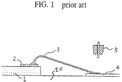
- FIG. 1 is a side view of a conventional wire-bonding structure between a bonding pad on a semiconductor device and a lead frame on a printed circuit board.
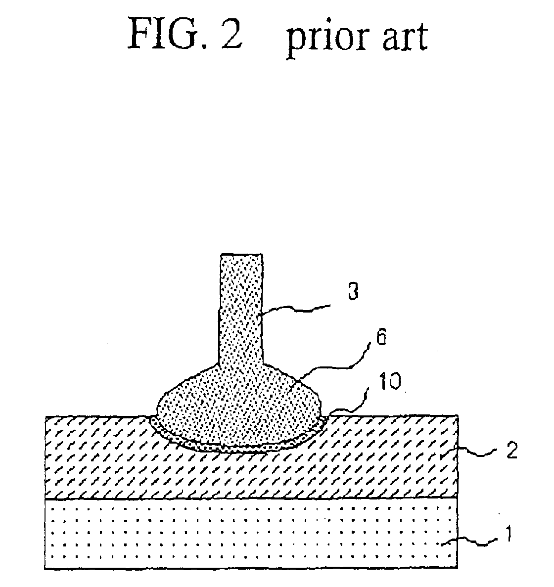
- FIG. 2 is a fragmentary cross sectional view of a bonding interface between a bonding wire and a bonding pad immediately after the bonding process and before the high output driving of the semiconductor device.
- FIG. 3 is a fragmentary cross sectional view of a bonding interface between a bonding wire and a bonding pad after the high output driving of the semiconductor device.
- bonding pads 2 having a thickness of about 1 micrometer are provided on a surface of a semiconductor device which is placed on a printed circuit board 10.
- the bonding pads 2 are bonded through bonding wires 3 to leads frames 4 of the printed circuit board 10.
- the bonding pads 2 are made of an Al-base material.
- the bonding wire 3 are made of an Au-base material.
- the bonding wire 3 has a ball 6 which is bonded with the bonding pad 2 by a thermal compression bonding.
- the bonding wire 3 is further bonded to the lead frame 4 by use of a bonding tool 5.
- the ball 6 of the bonding wire 3 digs into the bonding pad 2 by the thermal compression bonding, whereby an Au-Al alloy layer 10 is formed on a bonding interface between the ball 6 of the bonding wire 3 and the bonding pad 2.
- FIG. 3 illustrates the grown Au-Al alloy layer 10 on the bonding interface after the high output driving of the semiconductor device at a high temperature for a long time.
- the Au-Al alloy layer 10 is grown up to increase the thickness uniformly.
- the Au-Al alloy layer 10 is higher in resistivity than the bonding pad 2 and the bonding wire 3.
- the current flows through the Au-Al alloy layer 10 in the thickness direction, for which reasons the increase in thickness of the Au-Al alloy layer 10 incrcases the resistance, to which the current senses. Namely, the increase in thickness of the Au-Al alloy layer 10 increases the bonding resistance between the bonding pad 2 and the bonding wire 3. Further, a bonding deterioration also increases the bonding resistance between the bonding pad 2 and the bonding wire 3.
- the present invention provides a bonding structure between a bonding pad and a bonding portion of a bonding wire made of an Au-base material, wherein said bonding pad further comprises : a base layer; at least a barrier layer overlying said base layer ; and a bonding layer overlying said at least barrier layer, said bonding layer including an Al-base material, and wherein said bonding portion of said bonding wire is buried in said bonding layer, and an Au-Al alloy layer extends on an interface between said bonding portion and said bonding layer, and a bottom of said Au-Al alloy layer is in contact with or adjacent to an upper surface of said barrier layer.
- FIG. 1 is a side view of a conventional wire-bonding structure between a bonding pad on a semiconductor device and a lead frame on a printed circuit board.
- FIG. 2 is a fragmentary cross sectional view of a bonding interface between a bonding wire and a bonding pad immediately after the bonding process and before the high output driving of the semiconductor device.
- FIG. 3 is a fragmentary cross sectional view of a bonding interface between a bonding wire and a bonding pad after the high output driving of the semiconductor device.
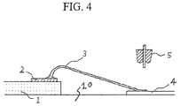
- FIG. 4 is a side view of a conventional wire-bonding structure between a bonding pad on a semiconductor device and a lead frame on a printed circuit board in a preferred embodiment in accordance with the present invention.
- FIG. 5 is a fragmentary cross sectional view of a bonding interface between a bonding wire and a bonding pad immediately after the bonding process and before the high output driving of the semiconductor device in a preferred embodiment in accordance with the present invention.
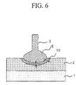
- FIG. 6 is a fragmentary cross sectional view of a bonding interface between a bonding wire and a bonding pad after the high output driving of the semiconductor device in a preferred embodiment in accordance with the present invention.
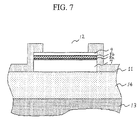
- FIG. 7 is a fragmentary cross sectional elevation view illustrative of a novel bonding pad over a semiconductor device in a preferred embodiment in accordance with the present invention.
- FIGS. 8A through 8F are fragmentary cross sectional elevation views illustrative of the bonding pad structures in sequential steps involved in the method of forming the bonding pad of FIG. 7 in a preferred embodiment in accordance with the present invention.
- FIG. 9 is a diagram showing respective resistance variations over times of six samples of the semiconductor devices with the different novel bonding pad structures in accordance with the present invention and one example of the semiconductor device with the conventional bonding pad structure of the prior art.
- FIG. 10 is a diagram showing respective resistance variation rates over times of six samples of the semiconductor devices with the different novel bonding pad structures in accordance with the present invention and a single comparative sample of the semiconductor device with the conventional bonding pad structure of the prior art.
- a first aspect of the present invention is a bonding structure between a bonding pad and a bonding portion of a bonding wire made of an Au-base material, wherein said bonding pad further comprises : a base layer ; at least a barrier layer overlying said base layer ; and a bonding layer overlying said at least barrier layer, said bonding layer including an Al-base material, and wherein said bonding portion of said bonding wire is buried in said bonding layer, and an Au-Al alloy layer extends on an interface between said bonding portion and said bonding layer, and a bottom of said Au-Al alloy layer is in contact with or adjacent to an upper surface of said barrier layer.
- a bottom portion of said Au-Al alloy layer under a bottom of said bonding portion is thinner than side portions of said Au-Al alloy layer adjacent to side portions of said bonding portion.
- said at least barrier layer includes at least one of Ti, W, Pt, Ta, Ni, and alloys thereof.
- said at least barrier layer has a thickness of at least 200 nanometers.
- said at least barrier layer comprises a bottom barrier layer made of Ti and a top barrier layer made of TiN.
- said bottom barrier layer and said top barrier layer have respective thicknesses which are at least 100 nanometers.
- said bonding layer has a thickness of at most 600 nanometers.
- a second aspect of the present invention is a bonding pad comprising : a base layer; at least a barrier layer overlying said base layer ; and a bonding layer overlying said at least barrier layer, said bonding layer including an Al-base material, and wherein said at least barrier layer comprises a martial which suppresses a formation of an Al-Au alloy.
- said at least barrier layer includes at least one of Ti, W, Pt, Ta, Ni, and alloys thereof.
- said at least barrier layer has a thickness of at least 200 nanometers.
- said at least barrier layer comprises a bottom barrier layer made of Ti and a top barrier layer made of TiN.
- said bottom barrier layer and said top barrier layer have respective thicknesses which are at least 100 nanometers.
- said bonding layer has a thickness of at most 600 nanometers.
- a third aspect of the present invention is a semiconductor device having at least a bonding pad which is bonded through a bonding wire of an Au-base material to a lead frame of a printed circuit board, on which said semiconductor device is mounted, wherein said bonding pad further comprises : a base layer ; at least a barrier layer overlying said base layer; and a bonding layer overlying said at least barrier layer, said bonding layer including an Al-base material, and wherein a bonding portion of said bonding wire is buried in said bonding layer, and an Au-Al alloy layer extends on an interface between said bonding portion and said bonding layer, and a bottom of said Au-Al alloy layer is in contact with or adjacent to an upper surface of said barrier layer.
- a bottom portion of said Au-Al alloy layer under a bottom of said bonding portion is thinner than side portions of said Au-Al alloy layer adjacent to side portions of said bonding portion.
- said at least barrier layer includes at least one of Ti, W, Pt, Ta, Ni, and alloys thereof.
- said at least barrier layer has a thickness of at least 200 nanometers.
- said at least barrier layer comprises a bottom barrier layer made of Ti and a top barrier layer made of TiN.
- said bottom barrier layer and said top barrier layer have respective thicknesses which are at least 100 nanometers.
- said bonding layer has a thickness of at most 600 nanometers.
- a fourth aspect of the present invention is a method of bonding a bonding portion of a bonding wire made of an Au-base material to a bonding pad, said bonding pad further comprising : a base layer ; at least a barrier layer overlying said base layer ; and a bonding layer overlying said at least barrier layer, said bonding layer including an Al-base material, said method comprising the step of : placing said bonding portion of said bonding wire over said bonding pad ; and carrying out a thermal compression bonding, so that said bonding portion of said bonding wire is buried in said bonding layer, and an Au-Al alloy layer is formed on an interface between said bonding portion and said bonding layer, wherein a bottom of said Au-Al alloy layer is in contact with or adjacent to an upper surface of said barrier layer.
- a bottom portion of said Au-Al alloy layer under a bottom of said bonding portion is thinner than side portions of said Au-Al alloy layer adjacent to side portions of said bonding portion.
- said at least barrier layer includes at least one of Ti, W, Pt, Ta, Ni, and alloys thereof.
- said at least barrier layer has a thickness of at least 200 nanometers.
- said at least barrier layer comprises a bottom barrier layer made of Ti and a top barrier layer made of TiN.
- said bottom barrier layer and said top barrier layer have respective thicknesses which are at least 100 nanometers.
- said bonding layer has a thickness of at most 600 nanometers.
- FIG. 4 is a side view of a conventional wire-bonding structure between a bonding pad on a semiconductor device and a lead frame on a printed circuit board in a preferred embodiment in accordance with the present invention.
- FIG. 5 is a fragmentary cross sectional view of a bonding interface between a bonding wire and a bonding pad immediately after the bonding process and before the high output driving of the semiconductor device in a preferred embodiment in accordance with the present invention.
- FIG. 6 is a fragmentary cross sectional view of a bonding interface between a bonding wire and a bonding pad after the high output driving of the semiconductor device in a preferred embodiment in accordance with the present invention.
- bonding pads 2 having a thickness of about 1 micrometer are provided on a surface of a semiconductor device which is placed on a printed circuit board 10.
- the bonding pads 2 are bonded through bonding wires 3 to leads frames 4 of the printed circuit board 10.
- the bonding pads 2 are made of an Al-base material.
- the bonding wire 3 are made of an Au-base material.
- the bonding wire 3 has a ball 6 which is bonded with the bonding pad 2 by a thermal compression bonding or a ultrasonic vibration.
- the bonding wire 3 is further bonded to the lead frame 4 by use of a bonding tool 5.
- the ball 6 of the bonding wire 3 digs into the bonding pad 2 by the thermal compression bonding, whereby an Au-Al alloy layer 10 is formed on a bonding interface between the ball 6 of the bonding wire 3 and the bonding pad 2.
- the bonding pad 2 has a triple-layered structure which comprises laminations of a base layer 7 on a top surface of the semiconductor device 1, a barrier layer 8 on the base layer 7, and a bonding layer 9 on the barrier layer 8. As illustrated in FIG. 5, the ball 6 of the bonding wire 3 digs into the bonding layer 9, wherein an Au-Al alloy layer 10 is formed on the bonding interface between the ball 6 and the bonding layer 9.
- the base layer 7 may be made of an Al-base material such as Al, Al-alloy
- a thickness of the base layer 7 may be substantially the same as a thickness of interconnections of the semiconductor device 1.
- the thickness of the base layer 7 may, for example, be about 1.4 micrometers.
- the base layer 7 does not provide any influences to the bonding resistance and the bonding strength, for which reason the material ad the thickness are optional.
- the barrier layer 8 may be made of a Ti-base material.
- the barrier layer 8 may comprise a titanium layer.
- the barrier layer 8 may comprise a titanium alloy layer, such as a Ti-N alloy layer.
- the barrier layer 8 may comprise laminations of a titanium layer and a titanium alloy layer.
- the barrier layer 8 is provided to contact an erosion of the Au-Al alloy layer 10 toward the base layer 7.
- a thickness of the barrier layer 8 is decided to be sufficient for suppressing or controlling the erosion of the Au-Al alloy layer 10 toward the base layer 7.
- the barrier layer 8 comprises laminations of a top Ti layer and a bottom TiN layer, then it is possible that the top Ti layer has a thickness in the range of about 100-200 nanometers and the bottom TiN layer has a thickness of about 100 nanometers. Titanium and titanium compounds are known materials for preventing impurity diffusions.
- the thickness of the barrier layer 8 is sufficient for keeping the barrier function even after the barrier layer 8 received a mechanical shock in the bonding process, for which reason the thickness of the barrier layer 8 is thicker than the minimum thickness necessary for controlling the impurity diffusion to the base layer 7.
- the thickness of the barrier layer 8 is thicker by at least about 200 nanometers than when the minimum necessary thickness of the barrier layer 8 for preventing or controlling the impurity diffusion to the base layer 7.
- the bonding layer 9 may be made of the same material as the base layer in view of a possible reduction of the manufacturing cost. Namely, the bonding layer 9 may be made of Al-base material. A thickness of the bonding layer 9 is decided so that a bottom of the ball 6 digging into the bonding layer 9 is positioned near a top surface the barrier layer 8, and a bottom of the Au-Al alloy layer 10 is in contact with or adjacent to the top surface the barrier layer 8. This thickness may depend on the diameter of the bonding wire, and the thermal compression bonding condition.
- the thickness of the bonding layer 9 is at most about 600 nanometers.
- FIG. 6 illustrates the grown Au-Al alloy layer 10 on the bonding interface between the bonding layer 9 and the ball 6 after the high output driving of the semiconductor device at a high temperature for a long time.
- the Au-Al alloy layer 10 is grown up to increase the thickness non-uniformly, because the growth in the downward direction of the Au-Al alloy layer 10 is prevented or controlled by the barrier layer 8.
- the Au-Al alloy layer 10 is limited by the top surface of the barrier layer 8.
- the Au-Al alloy layer 10 is grown up in lateral directions through the bonding layer 9 but the downward growth of the bottom portion of the Au-Al alloy layer 10 is strictly limited by the top surface of the barrier layer 8.
- the Au-Al alloy layer 10 is different in thickness, wherein the Au-Al alloy layer 10 under the bottom of the ball 6 is very thin but the Au-Al alloy layer 10 on the side portions of the ball 6 is relatively thick.
- the extremely thin thickness of the Au-Al alloy layer 10 under the bottom of the ball 6 provides a very low resistance, to which the current senses. Namely, the extremely thin thickness of the Au-Al alloy layer 10 under the bottom of the ball 6 provides a very low bonding resistance between the bonding pad 2 and the bonding wire 3. Further, a bonding deterioration also increases the bonding resistance between the bonding pad 2 and the bonding wire 3.
- the barrier layer 9 provides an extremely lowly resistive current path through the Au-Al alloy layer 10 between the bonding pad 2 and the bonding wire 3. Since the thickness of the Au-Al alloy layer 10 under the bottom of the ball 6 remains unchanged, then the bonding resistance by the Au-Al alloy layer 10 also substantially remains unchanged.
- the barrier layer 8 also provides an additional advantage in increasing the bonding strength between the bonding pad 2 and the bonding wire 3.
- the Ti-base material for the barrier layer 8 is higher in hardness than the Al-base materials and the Au-base material. Further, as described above, the thickness of the barrier layer 8 is thicker than the minimum necessary thickness for preventing that the Au-Al alloy is formed to reach the base layer 7. For these reasons, the applied ultrasonic power is likely to be propagated to the ball 6 in the thermal compression bonding process.
- the thick Ti-based layer is likely to have a micro-irregularity or a small roughness on its surface.
- the micro-irregularity or the small roughness of the surface of the thick Ti-based layer causes that the overlying bonding layer 9 also has the micro-irregularity or the small roughness on its surface. This provides a desirable effect of increasing the bonding strength between the bonding layer 9 and the ball 6.
- the surface roughness of the barrier layer 8 depends on the condition for forming the barrier layer 8, such as sputtering process conditions. It is preferable that the thickness of the barrier layer 8 is decided in consideration of both the bonding conditions and the deposition conditions.
- the above described novel structure of the bonding pads 2 may be applicable to various cases, provided that the bonding pads are bonded with the Au-based bonding wires by the thermal compression bonding process.
- the above described novel structure of the bonding pads 2 is suitable for the high output devices, particularly microwave amplifying devices such as Si-MOSFET and GaAs-MESFET.
- FIG. 7 is a fragmentary cross sectional elevation view illustrative of a novel bonding pad over a semiconductor device in a preferred embodiment in accordance with the present invention.
- a semiconductor device having a high output performance is formed over a silicon substrate 13.
- a silicon dioxide film 14 having a thickness of 3 micrometers overlies a top surface of the silicon substrate 13.
- a plurality of bonding pads are provided on a top surface of the silicon dioxide film 14.
- a passivation film 11 of SiON having a thickness of 900 nanometers is provided on the top surface of the silicon dioxide film 14 and also on side walls and top surface peripheral regions of each of the bonding pads 2.
- a center region of the top surface of each of the bonding pads 2 is exposed to an opening of the passivation film 11.
- the bonding pad 2 comprises a base layer 7, a bottom barrier layer 8a, a top barrier layer 8b and a bonding layer 9.
- the base layer 7 is provided on the silicon dioxide film 14.
- the base layer 7 is made of AlCu, wherein Al is a base material and Cu is added into the Al-base material.
- the base layer 7 has a thickness of 1.4 micrometers.
- the bottom barrier layer 8a overlies the base layer 7.
- the bottom barrier layer 8a is made of TiN.
- the bottom barrier layer 8a has a thickness of 100 nanometers.
- the top barrier layer 8b overlies the bottom barrier layer 8a.
- the top barrier layer 8b is made of Ti.
- the top barrier layer 8b has a thickness of 300 nanometers.
- the bonding layer 9 overlies the top barrier layer 8b.
- the bonding layer 9 is made of AlCu, wherein Al is a base material and Cu is added into the Al-base material.
- the bonding layer 9 has a thickness of 350 nanometers.
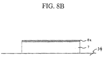
- FIGS. 8A through 8F are fragmentary cross sectional elevation views illustrative of the bonding pad structures in sequential steps involved in the method of forming the bonding pad of FIG. 7 in a preferred embodiment in accordance with the present invention.
- the base layer 7 made of AlCu is deposited on a top surface of the silicon dioxide layer 14 by a sputtering process for sputtering an AlCu-sputter target.
- the sputlering process is carried out under conditions of an Ar-gas flow rate of 75 sccm, a sputter power of 16.5kW, a deposition rate 225 angstroms per second. The deposition is discontinued until the thickness of the base layer 7 becomes 1.4 micrometers.
- the bottom barrier layer 8a made of TiN is deposited on a top surface of the base layer 7 by a subsequent sputtering process for sputtering a TiN-sputter target.
- the sputtering process is carried out under conditions of an Ar-gas flow rate of 34 sccm, a sputter power of 9.0kW, a deposition rate 22 angstroms per second. The deposition is discontinued until the thickness of the bottom barrier layer 8a becomes 100 nanometers.
- the top barrier layer 8b made of Ti is deposited on a top surface of the bottom barrier layer 8a by a subsequent sputtering process for sputtering a Ti-sputter target.
- the sputtering process is carried out under conditions of an Ar-gas flow rate of 29 sccm, a sputter power of 1.7kW, a deposition rate 18 angstroms per second. The deposition is discontinued until the thickness of the top barrier layer 8b becomes 300 nanometers.
- the bonding layer 9 made of AlCu is deposited on a top surface of the top barrier layer 8b by a subsequent sputtering process for sputtering an AlCu-sputter target.
- the sputtering process is carried out under conditions of an Ar-gas flow rate of 75 sccm, a sputter power of 16.5kW, a deposition rate 225 angstroms per second.
- the deposition is discontinued until the thickness of the bonding layer 9 becomes 350 nanometers. As a result, the lamination stricture of the bonding pad 2 is completed.
- the passivation film 11 made of SiON is deposited by a chemical vapor deposition method, so that the passivation film 11 covers the side walls and the top surface of the bonding pad 2 and the top surface of the silicon dioxide layer 14. The deposition is discontinued until the thickness of the passivation film 11 becomes 900 nanometers.
- a selective dry etching to the passivation film 11 is carried out to form an opening over a center region of the top surface of the bonding layer 9, thereby obtaining the structure as shown in FIG. 7.
- FIG. 9 is a diagram showing respective resistance variations over times of six samples of the semiconductor devices with the different novel bonding pad structures in accordance with the present invention and one example of the semiconductor device with the conventional bonding pad structure of the prior art.
- FIG. 10 is a diagram showing respective resistance variation rates over times of six samples of the semiconductor devices with the different novel bonding pad structures in accordance with the present invention and a single comparative sample of the semiconductor device with the conventional bonding pad structure of the prior art.
- the first to sixth samples of the improved bonding pad structures in accordance with the present invention and the comparative sample of the prior art have the following different lamination structures.
- the first sample of the improved bond pad has a three-layered structure which comprises an AlCu base layer having a thickness of 1400 nanometers, a TiN single barrier layer having a thickness of 100 nanometers, and an AlCu bonding layer having a thickness of 350 nanometers.
- the measured resistance values and the measured resistance variation rate values of the first sample are represented by a mark "- ⁇ -".
- the second sample of the improved bond pad has a four-layered structure which comprises an AlCu basc layer having a thickness of 1400 nanometers, a TiN bottom barrier layer having a thickness of 100 nanometers, a Ti top barrier layer having a thickness of 50 nanometers, and an AlCu bonding layer having a thickness of 350 nanometers.
- the measured resistance values and the measured resistance variation rate values of the second sample are represented by a mark "- ⁇ -".
- the third sample of the improved bond pad has a four-layered structure which comprises an AlCu base layer having a thickness of 1400 nanometers, a TiN bottom barrier layer having a thickness of 100 nanometers, a Ti top barrier layer having a thickness of 100 nanometers, and an AlCu bonding layer having a thickness of 100 nanometers.
- the measured resistance values and the measured resistance variation rate values of the third sample are represented by a mark "- ⁇ -".
- the fourth sample of the improved bond pad has a four-layered structure which comprises an AlCu base layer having a thickness of 1400 nanometers, a TiN bottom barrier layer having a thickness of 100 nanometers, a Ti top barrier layer having a thickness of 100 nanometers, and an AlCu bonding layer having a thickness of 350 nanometers.
- the measured resistance values and the measured resistance variation rate values of the fourth sample are represented by a mark "- ⁇ -".
- the fifth sample of the improved bond pad has a four-layered structure which comprises an AlCu base layer having a thickness of 1400 nanometers, a TiN bottom barrier layer having a thickness of 100 nanometers, a Ti top barrier layer having a thickness of 100 nanometers, and an AlCu bonding layer having a thickness of 600 nanometers.
- the measured resistance values and the measured resistance variation rate values of the fifth sample are represented by a mark "- ⁇ -".
- the sixth sample of the improved bond pad has a four-layered structure which comprises an AlCu base layer having a thickness of 1400 nanometers, a TiN bottom barrier layer having a thickness of 100 nanometers, a Ti top barrier layer having a thickness of 300 nanometers, and an AlCu bonding layer having a thickness of 350 nanometers.
- the measured resistance values and the measured resistance variation rate values of the sixth sample are represented by a mark "-•-".
- the comparative sample of the conventional bond pad has a single-layered structure which comprises an AlCu layer having a thickness of 1400 nanometers.
- the measured resistance values and the measured resistance variation rate values of the comparative sample are represented by a mark "- -".
- the resistance value gradually increases until the time reaches 500 hours.
- the resistance value remarkably increases as the time passes over 500 hours.
- the resistance variation rate value gradually increases until the time reaches 340 hours.
- the resistance variation rate value remarkably increases as the time passes over 340 hours.
- the resistance value substantially remains unchanged over times.
- the resistance variation rate value also substantially remains unchanged until the time reaches 168 hours, and gradually increases as the time passes over 168 hours.
- the resistance value substantially remains unchanged over times.
- the resistance variation rate value also substantially remains unchanged until the time reaches 500 hours, and slightly increases as the time passes over 500 hours.
- the resistance value substantially remains unchanged over times.
- the resistance variation rate value also substantially remains unchanged over times.
- the resistance value substantially remains unchanged over times.
- the resistance variation rate value also substantially remains unchanged over times.
- the resistance value substantially remains unchanged over times.
- the resistance variation rate value also substantially remains unchanged over times.
- the resistance value substantially remains unchanged over times.
- the resistance variation rate value also substantially remains unchanged over times.
- the total thickness of the top and bottom barrier layers is 200 nanometers. In the sixth sample, the total thickness of the top and bottom barrier layers is 400 nanometers. As the total thickness of the barrier layers is large, the increment of the resistance value is low. Namely, the increase in the total thickness of the barrier layers keeps the resistance value to be low.
- the total thickness of the top and bottom barrier layers is 200 nanometers. In the sixth sample, the total thickness of the top and bottom barrier layers is 400 nanometers. As the total thickness of the barrier layers is large, the resistance variation rate value is low. Namely, the increase in the total thickness of the barrier layers keeps the resistance variation rate value to be low.
- the third, fourth and fifth samples have the same total thickness of the barrier layers, for which reason these three samples are compared to each other. Over times, the third, fourth and fifth samples represented by the marks "- ⁇ -" "- ⁇ -" and "- ⁇ -" have almost the same resistance values.
- the thickness of the bonding layer is 100 nanometers.
- the thickness of the bonding layer is 350 nanometers.
- the thickness of the bonding layer is 600 nanometers. In the range of the bonding layer thickness from 100 nanometers to 600 nanometers, the resistance value is independent from the bonding layer thickness.
- the third, fourth and fifth samples have the same total thickness of the barrier layers, for which reason these three samples are compared to each other. Over times, the third, fourth and fifth samples represented by the marks "- ⁇ -" "- ⁇ -" and "- ⁇ -" have almost the same resistance values.
- the thickness of the bonding layer is 100 nanometers.
- the thickness of the bonding layer is 350 nanometers.
- the thickness of the bonding layer is 600 nanometers. In the range of the bonding layer thickness from 100 nanometers to 600 nanometers, the resistance variation rate value is independent from the bonding layer thickness.
- the respective bonding strengths of the first to fifth samples and the comparative sample were investigated by a tensile strength test.
- four products were prepared to measure the tensile strengths.
- three products were prepared to measure the tensile strengths.
- the disconnection of the loop-top of the bonding wire means that the bonding wire is very well and securely bonded with the bonding pad. This further means that the lamination structure of the bonding pad is suitable very much for securely bonding the bonding wire with the bonding pad.
- the measured tensile strength value is high, this means that the bonding strength between the bonding wire and the bonding pad is high, and also the tensile strength of the bonding wire is also high and the tensile strength at the position near the ball-shaped expanded portion of the bonding wire is also high. If the measured tensile strength value is low, this means that the tensile strength of the bonding wire is also low, but does not means that the bonding strength between the bonding wire and the bonding pad is low.
- the disconnection of the bonding wire near its expanded portion having the ball-shape means that the bonding wire is well bonded with the bonding pad.
- the lamination structure of the bonding pad is suitable for securely bonding the bonding wire with the bonding pad.
- the measured tensile strength value is high, this means that the bonding strength between the bonding wire and the bonding pad is high, and also the tensile strength at the position near the ball-shaped expanded portion of the bonding wire is also high.
- the measured tensile strength value is low, this means that the tensile strength at the position near the ball-shaped expanded portion of the bonding wire is low, but does not means that the bonding strength between the bonding wire and the bonding pad is low.
- the peel of the bonding wire from the surface of the bonding pad means that the bonding wire is not good bonded with the bonding pad. This further means that the lamination structure of the bonding pad is unsuitable for securely bonding the bonding wire with the bonding pad.
- the fourth and fifth samples showed the better performances in the bonding strength between the bonding wire and the bonding pad.
- the first sample showed the non-good performance in the bonding strength between the bonding wire and the bonding pad.
- the bonding strength between the bonding wire and the bonding pad well depends on the thickness of the barrier layer. A large bonding strength between the bonding wire and the bonding pad well is likely to depend on the large thickness of the barrier layer.
- a preferable thickness of the barrier layer may be at least 200 nanometers in view of the sufficient bonding strength between the bonding wire and the bonding pad.
- the bonding pad has the lamination structure comprising the base layer 7, the barrier layer 8 and the bonding layer 9, wherein the thickness of the barrier layer 8 is sufficiently thick for preventing that the Au-Al alloy layer 10 is grown to reach the base layer 7, and also the bonding layer 9 has such a thickness that the bottom of the Au-Al alloy layer 10 is in contact with or adjacent to the upper surface of the barrier layer 8, whereby the barrier layer may prevents a further vertical growth of the Au-Al alloy layer 10 in a direction vertical to the upper surface of the barrier layer 8 under a high temperature condition, and the Au-Al alloy layer 10 has a thin portion which underlies the bottom of the ball 6 of the bonding wire 3 and overlies the upper surface of the barrier layer 8.
- the increase in the bonding resistance of the thin portion of the Au-Al alloy layer 10 between the bonding wire 3 and the bonding pad 2 is prevented. This allows the semiconductor device to have a high reliability for a long term.
- barrier layer 8 is so deposited as to have a large thickness with a rough surface and also to allow an efficient application of the thermal compression force to the ball 6 of the bonding wire 3, thereby to obtain a large bonding strength between the bonding wire 3 and the bonding pad 2.
- the barrier layer 8 is made of the Ti-base material. Any other materials may also be available if preventing that the Au-Al alloy layer 10 is grown to reach the base layer 7 and also having a sufficient hardness for allowing the efficient application of the thermal compression force to the ball 6 of the bonding wire 3.
- W-base materials, Pt-base materials, Ta-base materials, and Ni-base materials are also available.
Landscapes
- Wire Bonding (AREA)
- Internal Circuitry In Semiconductor Integrated Circuit Devices (AREA)
Abstract
Description
Claims (27)
- A bonding structure between a bonding pad and a bonding portion of a bonding wire made of an Au-base material,
characterized in that said bonding pad further comprises :a base layer;at least a barrier layer overlying said base layer ; anda bonding layer overlying said at least barrier layer, said bonding layer including an Al-base material, andthat said bonding portion of said bonding wire is buried in said bonding layer, and an Au-Al alloy layer extends on an interface between said bonding portion and said bonding layer, and a bottom of said Au-Al alloy layer is in contact with or adjacent to an upper surface of said barrier layer. - The bonding structure as claimed in claim 1, characterized in that a bottom portion of said Au-Al alloy layer under a bottom of said bonding portion is thinner than side portions of said Au-Al alloy layer adjacent to side portions of said bonding portion.
- The bonding structure as claimed in claim 1, characterized in that said at least barrier laycr includes at least one of Ti, W, Pt, Ta, Ni, and alloys thereof.
- The bonding structure as claimed in claim 1, characterized in that said at least barrier layer has a thickness of at least 200 nanometers.
- The bonding structure as claimed in claim 1, characterized in that said at least barrier layer comprises a bottom barrier layer made of Ti and a top barrier layer made of TiN.
- The bonding structure as claimed in claim 5, characterized in that said bottom barrier layer and said top barrier layer have respective thicknesses which are at least 100 nanometers.
- The bonding structure as claimed in claim 1, characterized in that said bonding layer has a thickness of at most 600 nanometers.
- A bonding pad comprising :characterized in that said at least barrier layer comprises a martial which suppresses a formation of an Al-Au alloy.a base layer;at least a barrier layer overlying said base layer; anda bonding layer overlying said at least barrier layer, said bonding layer including an Al-base material, and
- The bonding structure as claimed in claim 8, characterized in that said at least barrier layer includes at least one of Ti, W, Pt, Ta, Ni, and alloys thereof.
- The bonding structure as claimed in claim 8, characterized in that said at least barrier layer has a thickness of at least 200 nanometers.
- The bonding structure as claimed in claim 8, characterized in that said at least barrier layer comprises a bottom barrier layer made of Ti and a top barrier layer made of TiN.
- The bonding structurc as claimed in claim 11, characterized in that said bottom barrier layer and said top barrier layer have respective thicknesses which are at least 100 nanometers.
- The bonding structure as claimed in claim 8, characterized in that said bonding layer has a thickness of at most 600 nanometers.
- A semiconductor device having at least a bonding pad which is bonded through a bonding wire of an Au-base material to a lead frame of a printed circuit board, on which said semiconductor device is mounted,
characterized in that said bonding pad further comprises :a base layer;at least a barrier layer overlying said base layer; anda bonding layer overlying said at least barrier layer, said bonding layer including an Al-base material, andthat a bonding portion of said bonding wire is buried in said bonding layer, and an Au-Al alloy layer extends on an interface between said bonding portion and said bonding layer, and a bottom of said Au-Al alloy layer is in contact with or adjacent to an upper surface of said barrier layer. - The semiconductor device as claimed in claim 14, characterized in that a bottom portion of said Au-Al alloy layer under a bottom of said bonding portion is thinner than side portions of said Au-Al alloy layer adjacent to side portions of said bonding portion.
- The semiconductor device as claimed in claim 14, characterized in that said at least barrier layer includes at least one of Ti, W, Pt, Ta, Ni, and alloys thereof.
- The semiconductor device as claimed in claim 14, characterized in that said at least barrier layer has a thickness of at least 200 nanometers.
- The semiconductor device as claimcd in claim 14, characterized in that said at least barrier layer comprises a bottom barrier layer made of Ti and a top barrier layer made of TiN.
- The semiconductor device as claimed in claim 18, characterized in that said bottom barrier layer and said top barrier layer have respective thicknesses which are at least 100 nanometers.
- The semiconductor device as claimed in claim 14, characterized in that said bonding layer has a thickness of at most 600 nanometers.
- A method of bonding a bonding portion of a bonding wire made of an Au-base material to a bonding pad, said bonding pad further comprising : a base layer ; at least a barrier layer overlying said base layer; and a bonding layer overlying said at least barrier layer, said bonding layer including an Al-base material,characterized in that a bottom of said Au-Al alloy layer is in contact with or adjacent to an upper surface of said barrier layer.said method comprising the step of:placing said bonding portion of said bonding wire over said bonding pad; andcarrying out a thermal compression bonding, so that said bonding portion of said bonding wire is buried in said bonding layer, and an Au-Al alloy layer is formed on an interface between said bonding portion and said bonding layer,
- The method as claimed in claim 21, characterized in that a bottom portion of said Au-Al alloy layer under a bottom of said bonding portion is thinner than side portions of said Au-Al alloy layer adjacent to side portions of said bonding portion.
- The method as claimed in claim 21, characterized in that said at least barrier layer includes at least one of Ti, W, Pt, Ta, Ni, and alloys thereof.
- The method as claimed in claim 21, characterized in that said at least barrier layer has a thickness of at least 200 nanometers.
- The method as claimed in claim 21, characterized in that said at least barrier layer comprises a bottom barrier layer made of Ti and a top barrier layer made of TiN.
- The method as claimed in claim 25, characterized in that said bottom barrier layer and said top barrier layer have respective thicknesses which are at least 100 nanometers.
- The method as claimed in claim 21, characterized in that said bonding layer has a thickness of at most 600 nanometers.
Applications Claiming Priority (2)
| Application Number | Priority Date | Filing Date | Title |
|---|---|---|---|
| JP2000264808A JP2002076051A (en) | 2000-09-01 | 2000-09-01 | Bonding pad structure and bonding method for semiconductor device |
| JP2000264808 | 2000-09-01 |
Publications (2)
| Publication Number | Publication Date |
|---|---|
| EP1187200A2 true EP1187200A2 (en) | 2002-03-13 |
| EP1187200A3 EP1187200A3 (en) | 2004-03-31 |
Family
ID=18752169
Family Applications (1)
| Application Number | Title | Priority Date | Filing Date |
|---|---|---|---|
| EP01120591A Withdrawn EP1187200A3 (en) | 2000-09-01 | 2001-08-29 | Semiconductor device with an improved bonding pad structure |
Country Status (4)
| Country | Link |
|---|---|
| US (2) | US20020027289A1 (en) |
| EP (1) | EP1187200A3 (en) |
| JP (1) | JP2002076051A (en) |
| KR (1) | KR20020018628A (en) |
Cited By (1)
| Publication number | Priority date | Publication date | Assignee | Title |
|---|---|---|---|---|
| EP2685511A4 (en) * | 2011-03-10 | 2014-08-13 | Dowa Electronics Materials Co Ltd | SEMICONDUCTOR LIGHT-EMITTING ELEMENT, AND MANUFACTURING METHOD THEREOF |
Families Citing this family (33)
| Publication number | Priority date | Publication date | Assignee | Title |
|---|---|---|---|---|
| EP1025217B1 (en) * | 1997-10-24 | 2006-10-04 | Invitrogen Corporation | Recombinational cloning using nucleic acids having recombination sites |
| JP3943416B2 (en) * | 2002-03-07 | 2007-07-11 | 株式会社ルネサステクノロジ | Manufacturing method of semiconductor device |
| JP2003303848A (en) | 2002-04-12 | 2003-10-24 | Nec Compound Semiconductor Devices Ltd | Semiconductor device |
| US8896397B2 (en) * | 2003-04-16 | 2014-11-25 | Intellectual Ventures Fund 77 Llc | Surface acoustic wave device and method of adjusting LC component of surface acoustic wave device |
| JP4381714B2 (en) * | 2003-04-16 | 2009-12-09 | Okiセミコンダクタ株式会社 | Surface acoustic wave device, surface acoustic wave device, and method of manufacturing surface acoustic wave device |
| JP2005086118A (en) * | 2003-09-11 | 2005-03-31 | Renesas Technology Corp | Semiconductor device |
| US7015580B2 (en) * | 2003-11-25 | 2006-03-21 | International Business Machines Corporation | Roughened bonding pad and bonding wire surfaces for low pressure wire bonding |
| JP4513440B2 (en) * | 2004-07-15 | 2010-07-28 | 住友ベークライト株式会社 | Semiconductor device |
| US7183656B2 (en) * | 2005-01-25 | 2007-02-27 | International Business Machines Corporation | Bilayer aluminum last metal for interconnects and wirebond pads |
| JP4639138B2 (en) * | 2005-10-28 | 2011-02-23 | パナソニック株式会社 | Semiconductor device |
| US7656045B2 (en) * | 2006-02-23 | 2010-02-02 | Freescale Semiconductor, Inc. | Cap layer for an aluminum copper bond pad |
| US7598164B2 (en) * | 2006-10-12 | 2009-10-06 | Technion Research & Development Foundation Ltd. | Method for direct bonding of metallic conductors to a ceramic substrate |
| KR100860445B1 (en) | 2007-07-05 | 2008-09-25 | 주식회사 케이이씨 | Semiconductor device and manufacturing method of bond pad |
| TWI372453B (en) * | 2008-09-01 | 2012-09-11 | Advanced Semiconductor Eng | Copper bonding wire, wire bonding structure and method for processing and bonding a wire |
| TW201030916A (en) * | 2009-02-11 | 2010-08-16 | Advanced Semiconductor Eng | Pad and package structure using the same |
| US8531022B2 (en) * | 2009-03-06 | 2013-09-10 | Atmel Corporation | Routable array metal integrated circuit package |
| US8101871B2 (en) * | 2009-05-26 | 2012-01-24 | Lsi Corporation | Aluminum bond pads with enhanced wire bond stability |
| JP5072948B2 (en) * | 2009-06-03 | 2012-11-14 | 三菱電機株式会社 | Semiconductor device |
| US8455304B2 (en) * | 2010-07-30 | 2013-06-04 | Atmel Corporation | Routable array metal integrated circuit package fabricated using partial etching process |
| KR101195265B1 (en) | 2010-09-09 | 2012-11-14 | 에스케이하이닉스 주식회사 | Method for wire bonding |
| JP5882014B2 (en) * | 2011-10-04 | 2016-03-09 | エスアイアイ・セミコンダクタ株式会社 | Semiconductor device |
| JP6074984B2 (en) | 2012-09-28 | 2017-02-08 | ローム株式会社 | Semiconductor device |
| US8767351B1 (en) * | 2013-01-31 | 2014-07-01 | Seagate Technology Llc | Ambient temperature ball bond |
| US20150048509A1 (en) * | 2013-08-16 | 2015-02-19 | Globalfoundries Singapore Pte. Ltd. | Cmos compatible wafer bonding layer and process |
| US20150057602A1 (en) * | 2013-08-26 | 2015-02-26 | Roger Alan Mason | System and Method for Administering Peritoneal Dialysis |
| JP6420721B2 (en) | 2014-07-09 | 2018-11-07 | ルネサスエレクトロニクス株式会社 | Semiconductor device and manufacturing method thereof |
| JP2016028417A (en) | 2014-07-11 | 2016-02-25 | ローム株式会社 | Electronic equipment |
| JP6377981B2 (en) | 2014-07-11 | 2018-08-22 | ローム株式会社 | Electronic equipment |
| US9960130B2 (en) * | 2015-02-06 | 2018-05-01 | UTAC Headquarters Pte. Ltd. | Reliable interconnect |
| JP6607771B2 (en) | 2015-12-03 | 2019-11-20 | ローム株式会社 | Semiconductor device |
| JP6931869B2 (en) * | 2016-10-21 | 2021-09-08 | 国立研究開発法人産業技術総合研究所 | Semiconductor device |
| JP2020072169A (en) | 2018-10-31 | 2020-05-07 | ルネサスエレクトロニクス株式会社 | Semiconductor device and method of manufacturing semiconductor device |
| JP7562953B2 (en) * | 2020-02-14 | 2024-10-08 | 富士電機株式会社 | Semiconductor Module |
Family Cites Families (11)
| Publication number | Priority date | Publication date | Assignee | Title |
|---|---|---|---|---|
| US3585461A (en) * | 1968-02-19 | 1971-06-15 | Westinghouse Electric Corp | High reliability semiconductive devices and integrated circuits |
| US4093110A (en) * | 1977-03-11 | 1978-06-06 | Olin Corporation | Noise and fouling reducer for powder-actuated tool |
| DE3641524A1 (en) * | 1985-12-10 | 1987-06-11 | Mitsubishi Electric Corp | Method of fabricating a semiconductor component |
| JPS63148646A (en) * | 1986-12-12 | 1988-06-21 | Toshiba Corp | Semiconductor device |
| JPH02285638A (en) * | 1989-04-27 | 1990-11-22 | Toshiba Corp | Semiconductor device |
| US5455195A (en) * | 1994-05-06 | 1995-10-03 | Texas Instruments Incorporated | Method for obtaining metallurgical stability in integrated circuit conductive bonds |
| US5661081A (en) * | 1994-09-30 | 1997-08-26 | United Microelectronics Corporation | Method of bonding an aluminum wire to an intergrated circuit bond pad |
| DE69706194T2 (en) * | 1997-01-16 | 2002-07-04 | Ford Motor Co. Ltd., Brentwood | METHOD FOR DOPING A METAL CONNECTING WIRE |
| US5976964A (en) * | 1997-04-22 | 1999-11-02 | Micron Technology, Inc. | Method of improving interconnect of semiconductor device by utilizing a flattened ball bond |
| TW426980B (en) * | 1999-01-23 | 2001-03-21 | Lucent Technologies Inc | Wire bonding to copper |
| JP2000223527A (en) * | 1999-01-28 | 2000-08-11 | Mitsubishi Electric Corp | Semiconductor device |
-
2000
- 2000-09-01 JP JP2000264808A patent/JP2002076051A/en active Pending
-
2001
- 2001-08-29 EP EP01120591A patent/EP1187200A3/en not_active Withdrawn
- 2001-08-30 US US09/941,622 patent/US20020027289A1/en not_active Abandoned
- 2001-08-31 US US09/942,729 patent/US6507112B1/en not_active Expired - Fee Related
- 2001-09-01 KR KR1020010053695A patent/KR20020018628A/en not_active Abandoned
Cited By (2)
| Publication number | Priority date | Publication date | Assignee | Title |
|---|---|---|---|---|
| EP2685511A4 (en) * | 2011-03-10 | 2014-08-13 | Dowa Electronics Materials Co Ltd | SEMICONDUCTOR LIGHT-EMITTING ELEMENT, AND MANUFACTURING METHOD THEREOF |
| US9172005B2 (en) | 2011-03-10 | 2015-10-27 | Dowa Electronics Materials Co., Ltd. | Semiconductor light emitting diode having a contact portion and a reflective portion |
Also Published As
| Publication number | Publication date |
|---|---|
| US6507112B1 (en) | 2003-01-14 |
| JP2002076051A (en) | 2002-03-15 |
| EP1187200A3 (en) | 2004-03-31 |
| KR20020018628A (en) | 2002-03-08 |
| US20020027289A1 (en) | 2002-03-07 |
Similar Documents
| Publication | Publication Date | Title |
|---|---|---|
| EP1187200A2 (en) | Semiconductor device with an improved bonding pad structure | |
| US7115985B2 (en) | Reinforced bond pad for a semiconductor device | |
| US7511363B2 (en) | Copper interconnect | |
| US20030119297A1 (en) | Metal redistribution layer having solderable pads and wire bondable pads | |
| KR100658547B1 (en) | Semiconductor device and manufacturing method thereof | |
| US5249728A (en) | Bumpless bonding process having multilayer metallization | |
| US8753972B2 (en) | Copper bonding compatible bond pad structure and method | |
| JP2003209134A (en) | Semiconductor device and manufacturing method thereof | |
| GB2362510A (en) | Wire bonding method for semiconductor devices | |
| JP2001015549A (en) | Semiconductor device and method of manufacturing the same | |
| JPH07114214B2 (en) | Semiconductor device | |
| US7656045B2 (en) | Cap layer for an aluminum copper bond pad | |
| US7327030B2 (en) | Apparatus and method incorporating discrete passive components in an electronic package | |
| JPH06177200A (en) | Formation of semiconductor integrated circuit device | |
| JPH11121458A (en) | Semiconductor device | |
| US6888258B2 (en) | Semiconductor device including copper interconnect line and bonding pad, and method of manufacturing the same | |
| JPH11163026A (en) | Wire bonding method | |
| JPH10163590A (en) | Stack-forming method for c-4 thin-film metallurgy | |
| JPH06333977A (en) | Semiconductor device and manufacturing method thereof | |
| JP2757780B2 (en) | Semiconductor device | |
| US6982493B2 (en) | Wedgebond pads having a nonplanar surface structure | |
| JP2000299349A (en) | Method for manufacturing semiconductor device | |
| JPH08124929A (en) | Semiconductor integrated circuit device and manufacturing method thereof | |
| JP2001244268A (en) | Integrated circuit | |
| JP2987905B2 (en) | Semiconductor device |
Legal Events
| Date | Code | Title | Description |
|---|---|---|---|
| PUAI | Public reference made under article 153(3) epc to a published international application that has entered the european phase |
Free format text: ORIGINAL CODE: 0009012 |
|
| AK | Designated contracting states |
Kind code of ref document: A2 Designated state(s): AT BE CH CY DE DK ES FI FR GB GR IE IT LI LU MC NL PT SE TR |
|
| AX | Request for extension of the european patent |
Free format text: AL;LT;LV;MK;RO;SI |
|
| RAP1 | Party data changed (applicant data changed or rights of an application transferred) |
Owner name: NEC COMPOUND SEMICONDUCTOR DEVICES, LTD. |
|
| PUAL | Search report despatched |
Free format text: ORIGINAL CODE: 0009013 |
|
| AK | Designated contracting states |
Kind code of ref document: A3 Designated state(s): AT BE CH CY DE DK ES FI FR GB GR IE IT LI LU MC NL PT SE TR |
|
| AX | Request for extension of the european patent |
Extension state: AL LT LV MK RO SI |
|
| 17P | Request for examination filed |
Effective date: 20040217 |
|
| 17Q | First examination report despatched |
Effective date: 20040510 |
|
| AKX | Designation fees paid |
Designated state(s): DE FI FR IT NL SE |
|
| STAA | Information on the status of an ep patent application or granted ep patent |
Free format text: STATUS: THE APPLICATION IS DEEMED TO BE WITHDRAWN |
|
| 18D | Application deemed to be withdrawn |
Effective date: 20041123 |