EP1184889A1 - Indexröhre - Google Patents
Indexröhre Download PDFInfo
- Publication number
- EP1184889A1 EP1184889A1 EP01000408A EP01000408A EP1184889A1 EP 1184889 A1 EP1184889 A1 EP 1184889A1 EP 01000408 A EP01000408 A EP 01000408A EP 01000408 A EP01000408 A EP 01000408A EP 1184889 A1 EP1184889 A1 EP 1184889A1
- Authority
- EP
- European Patent Office
- Prior art keywords
- conductor tracks
- cathode ray
- ray tube
- layer
- electrically insulating
- Prior art date
- Legal status (The legal status is an assumption and is not a legal conclusion. Google has not performed a legal analysis and makes no representation as to the accuracy of the status listed.)
- Withdrawn
Links
Images
Classifications
-
- H—ELECTRICITY
- H01—ELECTRIC ELEMENTS
- H01J—ELECTRIC DISCHARGE TUBES OR DISCHARGE LAMPS
- H01J31/00—Cathode ray tubes; Electron beam tubes
- H01J31/08—Cathode ray tubes; Electron beam tubes having a screen on or from which an image or pattern is formed, picked up, converted, or stored
- H01J31/10—Image or pattern display tubes, i.e. having electrical input and optical output; Flying-spot tubes for scanning purposes
- H01J31/20—Image or pattern display tubes, i.e. having electrical input and optical output; Flying-spot tubes for scanning purposes for displaying images or patterns in two or more colours
-
- H—ELECTRICITY
- H01—ELECTRIC ELEMENTS
- H01J—ELECTRIC DISCHARGE TUBES OR DISCHARGE LAMPS
- H01J9/00—Apparatus or processes specially adapted for the manufacture, installation, removal, maintenance of electric discharge tubes, discharge lamps, or parts thereof; Recovery of material from discharge tubes or lamps
- H01J9/20—Manufacture of screens on or from which an image or pattern is formed, picked up, converted or stored; Applying coatings to the vessel
-
- H—ELECTRICITY
- H01—ELECTRIC ELEMENTS
- H01J—ELECTRIC DISCHARGE TUBES OR DISCHARGE LAMPS
- H01J2231/00—Cathode ray tubes or electron beam tubes
- H01J2231/12—CRTs having luminescent screens
- H01J2231/121—Means for indicating the position of the beam, e.g. beam indexing
Definitions
- the invention relates to a cathode ray tube equipped with a color screen, an electron gun for emitting at least one electron beam and one Deflection device, the color screen comprising a first set of conductive traces and a second set of conductor tracks, a phosphor layer applied thereon, and further a means for receiving signals generated by the conductor tracks, and has a means for forwarding correction signals to the deflection device.
- a color cathode ray tube has a color screen, a neck and a color screen cone connecting to the neck and a cone provided inside the neck Electron gun for emitting at least one electron beam.
- the color screen has a phosphor layer in which the red, green or blue emitting phosphors are either vertical Strip triple or in the pattern of triangles arranged in a triangle To make sure that each of the three electron beams is only for him certain phosphors, there is a so-called shadow mask close to the color screen appropriate.
- Each triple of fluorescent is exactly one opening in the shadow mask, for example, a slot or a hole, assigned by the three at the same time Pass the electron beam through at slightly different angles.
- a disadvantage of such a shadow mask is that almost 80% of the electrons do not get through the shadow mask, but rather hit the shadow mask and are then removed.
- Another disadvantage of a shadow mask is that microphone effects can occur during operation.
- a shadow mask can warp during operation due to the resulting heating, and the openings of the shadow mask no longer sit in the correct positions.
- a cathode ray tube with an arrangement for electron beam control is known, in which the position of the electron beam is determined by arranging conductor tracks under each fluorescent strip. The position of the electron beam can be determined from the measured current difference between two adjacent conductor tracks and, if necessary, a correction can be made.
- Such cathode ray tubes are also referred to as index tubes.
- the color selection is independent of the diameter of the respective electron beam.
- a big disadvantage of the index tubes is that that the electron beam cannot be of any size and only excite a fluorescent line may, since otherwise no clear position of the electron beam can be determined.
- the electron beam diameter is at most equal to the width the fluorescent line plus the width of the areas of a black matrix that are on both Sides next to the fluorescent line.
- a cathode ray tube equipped with a color screen, an electron gun for emitting at least one electron beam and a deflection device, the color screen comprising a front plate, a first set of conductor tracks and a second set of conductor tracks, a phosphor layer applied thereon, and furthermore a means for Receiving signals generated by the conductor tracks and having a means for forwarding correction signals to the deflection device, the conductor tracks being partially covered with an electrically insulating layer. It is preferred that the electrically insulating layer is applied in strip-shaped sections on the conductor tracks.
- one Layer becomes a current equalization between two conductor tracks by electron conduction phenomena difficult or prevented in the phosphor layer.
- the strip-shaped sections on the conductor tracks have a minimum size.
- the portions not covered with an electrically insulating layer the conductor tracks are widened.
- the measured Current signal can be increased.
- the currents flowing through the phosphor layer get to the conductor tracks and generate a current signal there are reproducible. So for example, the current signal should not be too small to accommodate changes in the measured Being able to clearly identify and assign current differences.
- strip-shaped sections of the electrically insulating layer on a conductor track offset to the strip-shaped sections of the electrical insulating layer are arranged on an adjacent conductor track.
- the portions of the electrically insulating layer are two neighboring conductor tracks are not completely offset, but in one Area of length X are arranged to overlap.
- an aluminum layer is applied to the phosphor layer is.
- the thin aluminum layer on the fluorescent layer acts as a mirror and reflects Visible light radiated inwards into the tube towards the front plate wind increases the efficiency of the index tube.
- the color screen additionally has a dielectric layer between the aluminum layer and the conductor tracks.
- the dielectric layer prevents short circuits in which aluminum through the Fluorescent layer reaches the conductor tracks during the aluminization of the Form color screen and the entire color screen becomes unusable.
- the dielectric layer extends over the entire Extends inner surface of the color screen.
- the refractive index of the dielectric layer is lower than the refractive index of the Screen glass, can be applied by applying the dielectric layer over the entire Inner surface of the color screen reduces the amount of specularly reflected light become. This increases the luminance of the index tube and / or prevents the occurrence of disturbing external reflections.
- the dielectric layer is between the conductor tracks and the electrically insulating layer applied.
- the dielectric layer is applied between the phosphor layer and the aluminum layer.
- aluminum is prevented from coming into contact with the conductor tracks.
- the dielectric layer does not affect the current detection of the conductor tracks.
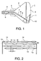
- the cathode ray tube shown in Fig. 1 is a color cathode ray tube 1 which has a color screen 2, a Neck 3 and a cone 4 which connects the color screen 2 and the neck 3 to one another, having. Inside the neck 3 there is an electron gun 6 which three electron beams 7, 8, 9 generated. The latter spread in this embodiment a color cathode ray tube 1 in one plane, the in-line plane, and on their way to the color screen 2 by a deflection device 5 horizontally and vertically deflected.
- the color screen 2 has a front panel 10 on which a first and a second set of conductor tracks, which are not shown in FIG. 1, applied are.
- a phosphor layer 11 is located on the conductor tracks.
- the phosphor layer 11 contains red, green and blue emitting phosphors, which in the form of horizontal strip triplets are applied.
- the color cathode ray tube 1, in particular the color screen 2 can have more Features such as a black matrix or an aluminum layer, which on the phosphor layer 11 is applied.
- the color screen 2 has an aluminum layer on, it can be advantageous that between the conductor tracks and the phosphor layer 11 or between phosphor layer 11 and the aluminum layer additionally one dielectric layer is applied. This dielectric layer can either only in the Area of the conductor tracks or over the entire inner surface area of the color screen 2 be applied.
- the dielectric layer is so thin that it is penetrated by fast electrons can be and so does not interfere with the current detection. In the places of dielectric Layer on which the electron beam is located is therefore conductive.
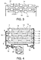
- the conductor tracks 12, 13 are horizontal and alternately applied to a front panel 10 of a color screen 2.
- the conductor tracks 12, 13 can be a metal such as Al and / or a conductive oxide such as for example ITO included.
- the respective conductor tracks 12, 13 are on sections covered with an electrically insulating layer 14.
- the striped sections of the electrically insulating layer 14 have a length L, for which the following applies: L> 3 x D, where D corresponds to the distance of the conductor tracks.
- the sections are wider than are the traces 12, 13 that cover them. As shown in Fig. 3, they cannot covered portions of the conductor tracks 12, 13 are widened to a larger current signal to obtain.
- the widenings are preferably optically transparent and contain for example ITO.
- the strip-shaped sections the electrically insulating layer 14 of a conductor track 12 offset from the strip-shaped Portions of the electrically insulating layer 14 on the adjacent conductor tracks 13 are arranged. It is advantageous that the strip-shaped sections of two Adjacent conductor tracks 12, 13 run parallel and overlap along an area. It is preferred for the length X of the area that X> D.
- the electrically insulating layer 14 can contain, for example, an oxide such as SiO 2 , MgO, Al 2 O 3 , TiO 2 or Ta 2 O 5 .
- the particles of the oxides mentioned preferably have a particle diameter between 0.5 and 5 ⁇ m and the layer thickness of the electrically insulating layer 14 is advantageously between 3 and 50 ⁇ m.
- a black pigment, for example carbon black, a ferrite or a spinel, with an approximately the same or smaller particle diameter can also be added to the oxides.
- An arrangement for determining the position of three electron beams is shown in FIG.
- the phosphor layer 11, which contains red, green and blue emitting phosphors in the form of individual fluorescent lines 15, 16, 17, is located on an arrangement of conductor tracks 12, 13.
- the phosphor layer 11 can also completely cover the conductor tracks 12, 13.
- Y 2 O 2 S: Eu can be used as the red-emitting phosphor
- ZnS: Ag as the blue-emitting phosphor
- ZnS: Cu gold
- Au can be used as the green-emitting phosphor.
- the individual fluorescent lines 15, 16 or 17 are each excited by an electron beam 7, 8 or 9. So that the electron beams 7, 8, 9 each excite only one fluorescent line 15, 16, 17 in a horizontal scan, the electron beams 7, 8, 9 are not arranged directly one below the other, but offset by a fluorescent line.
- a current signal 18 is generated on a conductor track 12 of the first set of conductor tracks and a current signal 19 on a conductor track 13 of the second set of conductor tracks.
- a means for receiving signals generated by the conductor tracks 12, 13 generates a differential current signal 20, by means of which the position of the electron beams 7, 8 and 9 can be determined. If the differential current signal 20 is zero, then the electron beams 7, 8 and 9 are exactly in the middle of the corresponding fluorescent line 15, 16, 17. If the differential current signal 20 has a positive or negative value, the electron beams 7, 8 and 9 are up or down shifted below in the fluorescent line 15, 16 and 17.
- the position of the electron beams 7, 8 or 9 can be corrected by a means for forwarding correction signals to the deflection device. Whether the electron beams 7, 8 and 9 in the fluorescent lines 15, 16 and 17 are shifted up or down with a positive value for the differential current signal 20 depends on the detector electronics used, which is used as a means for receiving signals.
- the detector electronics can be kept simple by simultaneously determining the position of all three electron beams 7, 8 and 9 by means of a signal.
- the measured current signals 18, 19 and therefore also the differential current signal 20 are larger and thus more reproducible. Furthermore, this prevents that if the displayed image has many black pixels, no differential current signal 20 is measured and thus no deviation in the electron beam positions can be detected.
- the color cathode ray tube 1 has a correction system which controls and corrects the position of the electron beams 7, 8 and 9 relative to one another. This correction system prevents the case in which only the position of an electron beam 7, 8 or 9 changes and all three electron beams 7, 8 and 9 as a whole are corrected by a measured differential current signal 20.
- the cathode ray tube works analogously in cathode ray tubes that use an electron beam, work with two or more electron beams.
- the procedure described can also be used in monochrome cathode ray tubes.
- a color screen 2 are first on a front panel 10 made of glass the conductor tracks 12, 13 by means of vapor deposition and subsequent structuring applied.
- the conductor tracks 12, 13 can, for example, on the underside, the side facing the front panel 10, black anodized aluminum and on the top Aluminum included. Through the blackened undersides of the conductor tracks 12, 13 points the color screen 2 also has a black matrix. Should the uncovered areas of the Conductor tracks 12, 13 will be widened, ITO will not be on and / or next to the electrically insulating layer 14 covered areas applied.
- the phosphor layer 11 is covered with a thin organic film, for example made of polyacrylate, and then an aluminum layer with a layer thickness between 100 and 300 nm is applied.
- the organic film can have holes through which aluminum is applied directly to the phosphor layer 11. The organic layer is removed without residue when the entire color screen 2 is heated.
- an aqueous suspension of an inorganic colloid such as Al 2 O 3 , SiO 2 , ZnO 2 or ZrO 2 , can be produced with an average particle diameter between 20 and 150 nm. This suspension is applied either to the conductor tracks 12, 13 or to the phosphor layer 11 such that the dielectric layer has a layer thickness between 100 nm and 1 ⁇ m after drying.
- the dielectric layer can also be printed using suitable colloid printing inks or pastes, vapor deposition or sputtering.
- Such a color screen 2 is then used to build a color cathode ray tube 1.
- a color screen 2 were made of glass on a front panel 10 Evaporation process and subsequent structuring of the conductor tracks 12, 13 as horizontal Strips applied.
- the distance D between two adjacent conductor tracks 12, 13 was 200 ⁇ m.
- the conductor tracks 12, 13 contained on the underside, the side of the Front plate 10 is facing, black anodized aluminum and aluminum on the top.
- the width of the conductor tracks 12, 13 was in each case 200 ⁇ m.
- An electrically insulating layer 14 made of Ta 2 O 5 was evaporated onto the conductor tracks 12, 13.
- the desired structuring of the electrically insulating layer 14 was achieved by using a mask.
- the average particle diameter of the Ta 2 O 5 was 1 ⁇ m and the layer thickness of the electrically insulating layer 14 was 5 ⁇ m.
- the electrically insulating layer 14 was applied as horizontal, strip-shaped sections, the length L of which was 700 ⁇ m, to the conductor tracks 12, 13.
- the strip-shaped sections of two adjacent conductor tracks 12, 13 were not applied completely offset from one another, but overlapped in an area with a length X of 300 ⁇ m.
- the phosphor layer 11 which contained ZnS: Cu, Au, ZnS: Ag and Y 2 O 2 S: Eu as phosphors, was applied by means of screen printing.
- the conductor tracks 12 have been electrically connected to one another and the conductor tracks 13 have been electrically connected to one another.
- the two sets of conductor tracks were connected to a means for receiving signals generated by the conductor tracks and detector electronics. The latter could also send correction signals to the deflection device 5.
- Such a color screen 2 was together with a neck 3, the color screen 2 with the neck 3 connecting cone 4, a deflection device 5 and one provided in the interior of the neck 3 electron gun 6 for the emission of three electron beams 7,8,9 used to build a color cathode ray tube 1.
- the diameter each electron beam 7, 8, 9 was 500 ⁇ m.
- a color screen 2 was produced in the same way as described in embodiment 1, except that a thin organic film made of poly ( isobutyl methacrylate) was applied to the phosphor layer 11 in such a way that individual phosphor particles were not covered with the film made of polyacrylate. A 100 nm thick aluminum layer was then evaporated.
- a color screen 2 of this type was described analogously to Example 1 used to build a color cathode ray tube 1.
- a color screen 2 was produced analogously to that described in exemplary embodiment 2, except that after the conductor tracks 12, 13 had been applied to the inside of the front plate 10 with the conductor tracks 12, 13, an aqueous suspension of colloidal SiO 2 with an average particle diameter of 80 nm and a non-ionic surfactant was poured. A uniformly distributed layer was obtained by rotating the front plate 1. After the entire front plate 10 had been dried at 200 ° C., a dielectric layer with a layer thickness of 300 nm was obtained. The electrically insulating layer 14 made of Ta 2 O 5 was then evaporated onto the dielectric layer in the region of the conductor tracks 12, 13 and the color screen 2 was produced as described in exemplary embodiment 2.
- a color screen 2 of this type was described analogously to Example 1 used to build a color cathode ray tube 1.
- a color screen 2 was produced analogously to that described in exemplary embodiment 1, only that after the application of the electrically insulating layer 14 to the conductor tracks 12, 13, the areas of the conductor tracks 12, 13 not covered by deposition of ITO have been broadened.
- a color screen 2 of this type was described analogously to Example 1 used to build a color cathode ray tube 1.
- a front panel 10 was made of glass Black matrix of soot applied as horizontal stripes.
- vapor deposition and subsequent structuring were congruent on the black matrix Printed conductors 12, 13 made of Al.
- the distance D between two neighboring ones Conductor paths 12, 13 was 300 ⁇ m and the width of a conductor path was 100 ⁇ m.
- the electrically insulating layer 14 made of MgO and carbon black was evaporated onto the conductor tracks 12, 13.
- the desired structuring of the electrically insulating layer 14 was achieved by using a mask.
- the electrically insulating layer 14 was applied as horizontal, strip-shaped sections, the length L of which was 1000 ⁇ m, to the conductor tracks 12, 13.
- the strip-shaped sections of two adjacent conductor tracks 12, 13 were not applied completely offset from one another, but overlapped in an area with a length X of 400 ⁇ m.
- a thin organic film made of poly ( isobutyl methacrylate) was applied to the phosphor layer 11 in such a way that individual phosphor particles were not covered with the film made of polyacrylate.
- a 200 nm thick aluminum layer was then evaporated.
- the conductor tracks 12 have been electrically connected to one another and the conductor tracks 13 have been electrically connected to one another.
- the two sets of conductor tracks were connected to a means for receiving signals generated by the conductor tracks and detector electronics. The latter could also send correction signals to the deflection device 5.
- Such a color screen 2 was together with a neck 3, the color screen 2 with the neck 3 connecting cone 4, a deflection device 5 and an electron gun 6 provided inside the neck 3 for emitting three Electron beams 7, 8, 9 used to build a color cathode ray tube 1.
- the diameter of each electron beam was 400 ⁇ m.
Landscapes
- Engineering & Computer Science (AREA)
- Manufacturing & Machinery (AREA)
- Cathode-Ray Tubes And Fluorescent Screens For Display (AREA)
Abstract
Description
Aus der WO 00/38212 ist eine Kathodenstrahlröhre mit einer Anordnung zur Elektronenstrahlkontrolle bekannt, bei der die Position des Elektronenstrahls dadurch bestimmt wird, dass Leiterbahnen unter jedem Leuchtstoffstreifen angeordnet sind. Aus der gemessenen Stromdifferenz zwischen zwei benachbarten Leiterbahnen kann die Position des Elektronenstrahls bestimmt und gegebenenfalls eine Korrektur vorgenommen werden. Derartige Kathodenstrahlröhren werden auch als Indexröhren bezeichnet.
Es ist bevorzugt, dass die elektrisch isolierende Schicht in streifenförmigen Abschnitten auf den Leiterbahnen aufgebracht ist.
In beiden Ausführungsformen wird verhindert, dass Aluminium in Kontakt mit den Leiterbahnen gelangt. Die dielektrische Schicht beeinträchtigt nicht die Stromdetektion der Leiterbahnen.
- Fig. 1
- den Aufbau einer Kathodenstrahlröhre,
- Fig. 2, Fig. 3
- jeweils eine mögliche Anordnung der Leiterbahnen und
- Fig. 4
- eine Anordnung zur Positionsbestimmung von drei Elektronenstrahlen.
In dieser Ausführung ist es von Vorteil, dass die Farbkathodenstrahlröhre 1 ein Korrektur-System aufweist, welches die Position der Elektronenstrahlen 7, 8 und 9 zueinander kontrolliert und korrigiert. Dieses Korrektur-System verhindert den Fall, dass sich nur die Position eines Elektronenstrahls 7, 8 oder 9 verändert und durch ein gemessenes Differenzstromsignal 20 alle drei Elektronenstrahlen 7,8 und 9 als Ganzes korrigiert werden.
Soll der Farbbildschirm 2 noch zusätzlich eine dielektrische Schicht aufweisen, kann eine wässrige Suspension eines anorganischen Kolloids, wie beispielsweise Al2O3, SiO2, ZnO2 oder ZrO2, mit einem mittleren Teilchendurchmesser zwischen 20 und 150 nm hergestellt werden. Diese Suspension wird entweder auf die Leiterbahnen 12, 13 oder auf die Leuchtstoffschicht 11 derart aufgebracht, dass die dielektrische Schicht nach dem Trocknen eine Schichtdicke zwischen 100 nm und 1 µm aufweist.
Claims (12)
- Kathodenstrahlröhre ausgestattet mit einem Farbbildschirm (2), einer Elektronenkanone (6) zur Emission mindestens eines Elektronenstrahls (7, 8, 9) und einer Ablenkungsvorrichtung (5), wobei der Farbbildschirm (2) eine Frontplatte (10), einen ersten Satz Leiterbahnen und einen zweiten Satz Leiterbahnen, darauf aufgebracht eine Leuchtstoffschicht (11), sowie weiterhin ein Mittel zum Empfang von Signalen, die von den Leiterbahnen generiert werden, und ein Mittel zur Weitergabe von Korrektursignalen an die Ablenkvorrichtung (5) aufweist, wobei die Leiterbahnen (12, 13) partiell mit einer elektrisch isolierenden Schicht (14) bedeckt sind.
- Kathodenstrahlröhre nach Anspruch 1,
dadurch gekennzeichnet, dass die elektrisch isolierende Schicht (14) in streifenförmigen Abschnitten auf den Leiterbahnen (12, 13) aufgebracht ist. - Kathodenstrahlröhre nach Anspruch 2,
dadurch gekennzeichnet, dass für einen streifenförmigen Abschnitt gilt, dass L > 3 x D, wobei L die Länge des jeweiligen Abschnitts ist und D der Abstand zwischen zwei benachbarten Leiterbahnen (12, 13). - Kathodenstrahlröhre nach Anspruch 2,
dadurch gekennzeichnet, dass die nicht mit einer elektrisch isolierenden Schicht (14) bedeckten Abschnitte der Leiterbahnen (12, 13) verbreitert sind. - Kathodenstrahlröhre nach Anspruch 2,
dadurch gekennzeichnet, dass die streifenförmigen Abschnitte der elektrisch isolierenden Schicht (14) auf einer Leiterbahn (12, 13) versetzt zu den streifenförmigen Abschnitten der elektrisch isolierenden Schicht (14) auf einer benachbarten Leiterbahn (12, 13) angeordnet sind. - Kathodenstrahlröhre nach Anspruch 2,
dadurch gekennzeichnet, dass die Abschnitte der elektrisch isolierenden Schicht (14) von zwei benachbarten Leiterbahnen (12, 13) nicht vollständig versetzt angeordnet sind, sondern in einem Bereich der Länge X überlappend angeordnet sind. - Kathodenstrahlröhre nach Anspruch 6,
dadurch gekennzeichnet, dass für die Länge X des Bereichs gilt, dass X>D ist. - Kathodenstrahlröhre nach Anspruch 1,
dadurch gekennzeichnet, dass auf der Leuchtstoffschicht (11) eine Aluminiumschicht aufgebracht ist. - Kathodenstrahlröhre nach Anspruch 8,
dadurch gekennzeichnet, dass der Farbbildschirm (2) zusätzlich eine dielektrische Schicht zwischen der Aluminiumschicht und den Leiterbahnen (12, 13) aufweist. - Kathodenstrahlröhre nach Anspruch 9,
dadurch gekennzeichnet, dass sich die dielektrische Schicht über die gesamte Innenfläche des Farbbildschirms (2) erstreckt. - Kathodenstrahlröhre nach Anspruch 9,
dadurch gekennzeichnet, dass die dielektrische Schicht zwischen den Leiterbahnen (12, 13) und der elektrisch isolierenden Schicht (14) aufgebracht ist. - Kathodenstrahlröhre nach Anspruch 8,
dadurch gekennzeichnet, dass die dielektrische Schicht zwischen den Leuchtstoffschicht (11) und der Aluminiumschicht aufgebracht ist.
Applications Claiming Priority (2)
| Application Number | Priority Date | Filing Date | Title |
|---|---|---|---|
| DE10042728A DE10042728A1 (de) | 2000-08-31 | 2000-08-31 | Indexröhre |
| DE10042728 | 2000-08-31 |
Publications (1)
| Publication Number | Publication Date |
|---|---|
| EP1184889A1 true EP1184889A1 (de) | 2002-03-06 |
Family
ID=7654389
Family Applications (1)
| Application Number | Title | Priority Date | Filing Date |
|---|---|---|---|
| EP01000408A Withdrawn EP1184889A1 (de) | 2000-08-31 | 2001-08-28 | Indexröhre |
Country Status (6)
| Country | Link |
|---|---|
| EP (1) | EP1184889A1 (de) |
| JP (1) | JP2002093341A (de) |
| KR (1) | KR20020018091A (de) |
| CN (1) | CN1341949A (de) |
| DE (1) | DE10042728A1 (de) |
| TW (1) | TW518629B (de) |
Cited By (1)
| Publication number | Priority date | Publication date | Assignee | Title |
|---|---|---|---|---|
| WO2003092034A1 (en) * | 2002-04-23 | 2003-11-06 | Philips Intellectual Property & Standards Gmbh | Color cathode ray tube having uv-reflective coating |
Citations (1)
| Publication number | Priority date | Publication date | Assignee | Title |
|---|---|---|---|---|
| WO2000038212A1 (en) * | 1998-12-21 | 2000-06-29 | Koninklijke Philips Electronics N.V. | Cathode ray tube of the index type |
-
2000
- 2000-08-31 DE DE10042728A patent/DE10042728A1/de not_active Withdrawn
-
2001
- 2001-08-28 EP EP01000408A patent/EP1184889A1/de not_active Withdrawn
- 2001-08-28 CN CN01141021A patent/CN1341949A/zh active Pending
- 2001-08-29 KR KR1020010052374A patent/KR20020018091A/ko not_active Withdrawn
- 2001-08-29 JP JP2001259154A patent/JP2002093341A/ja active Pending
- 2001-10-08 TW TW090124829A patent/TW518629B/zh active
Patent Citations (1)
| Publication number | Priority date | Publication date | Assignee | Title |
|---|---|---|---|---|
| WO2000038212A1 (en) * | 1998-12-21 | 2000-06-29 | Koninklijke Philips Electronics N.V. | Cathode ray tube of the index type |
Cited By (1)
| Publication number | Priority date | Publication date | Assignee | Title |
|---|---|---|---|---|
| WO2003092034A1 (en) * | 2002-04-23 | 2003-11-06 | Philips Intellectual Property & Standards Gmbh | Color cathode ray tube having uv-reflective coating |
Also Published As
| Publication number | Publication date |
|---|---|
| JP2002093341A (ja) | 2002-03-29 |
| CN1341949A (zh) | 2002-03-27 |
| DE10042728A1 (de) | 2002-03-14 |
| TW518629B (en) | 2003-01-21 |
| KR20020018091A (ko) | 2002-03-07 |
Similar Documents
| Publication | Publication Date | Title |
|---|---|---|
| DE69402481T2 (de) | Feldemissionsanzeigevorrichtung | |
| DE60011166T2 (de) | Elektronenemittierendes Element und Bildausgabevorrichtung | |
| DE69430568T2 (de) | Flacher bildschirm mit innerer tragstruktur | |
| DE3853510T2 (de) | Elektronenstrahl-Emittiervorrichtung und mit einer solchen Vorrichtung betriebene Bildwiedergabevorrichtung. | |
| DE60129514T2 (de) | Organische Electrolumineszenzvorrichtung mit zusätzlichem Kathodenbusleiter | |
| DE4132151C2 (de) | Bildanzeigegerät | |
| DE19534075A1 (de) | Phosphor und Fluoreszenzanzeigevorrichtung | |
| DE3910005A1 (de) | Bildanzeigegeraet | |
| EP0012920B1 (de) | Leuchtschirm für Bildanzeigeröhren und Verfahren zu seiner Herstellung | |
| DE1958674B2 (de) | Flächenhafte Gasentladungs-Anzeigevorrichtung zur farbigen Darstellung elektrischer Signale und Verfahren zur Herstellung dieser Vorrichtung | |
| DE69916353T2 (de) | Anzeigevorrichtung | |
| DE69024917T2 (de) | Verfahren zur Herstellung einer Kathodenstrahlröhre | |
| DE10042427A1 (de) | Plasmabildschirm mit verbessertem Kontrast | |
| DE2653812A1 (de) | Flache bildwiedergaberoehre | |
| DE4310765A1 (de) | Verfahren zur Herstellung eines Dünnschicht-Elektrolumineszenzelements | |
| EP1184889A1 (de) | Indexröhre | |
| EP1187167B1 (de) | Farbbildschirm mit blauer Leuchtstoffschicht | |
| DE3407197A1 (de) | Kathodenstrahlroehre | |
| DE19542263A1 (de) | Farbkathodenstrahlröhre mit einer inneren magnetischen Abschirmung | |
| DE1015047B (de) | Bildschirm fuer Farbfernsehaufnahmeroehre | |
| DE19624656A1 (de) | Rasteraufbau einer Kathodenstrahlröhre | |
| EP1211712A2 (de) | Kathodenstrahlröhre mit Anordnung zur Elektronenstrahlkontrolle | |
| DE2825902A1 (de) | Flachanzeigevorrichtung | |
| EP1211711A2 (de) | Kathodenstrahlröhre mit Anordnung zur Elektronenstrahlkontrolle | |
| DE3036219A1 (de) | Flachbildschirm |
Legal Events
| Date | Code | Title | Description |
|---|---|---|---|
| PUAI | Public reference made under article 153(3) epc to a published international application that has entered the european phase |
Free format text: ORIGINAL CODE: 0009012 |
|
| AK | Designated contracting states |
Kind code of ref document: A1 Designated state(s): AT BE CH CY DE DK ES FI FR GB GR IE IT LI LU MC NL PT SE TR |
|
| AX | Request for extension of the european patent |
Free format text: AL;LT;LV;MK;RO;SI |
|
| RAP1 | Party data changed (applicant data changed or rights of an application transferred) |
Owner name: KONINKLIJKE PHILIPS ELECTRONICS N.V. Owner name: PHILIPS CORPORATE INTELLECTUAL PROPERTY GMBH |
|
| 17P | Request for examination filed |
Effective date: 20020906 |
|
| AKX | Designation fees paid |
Free format text: DE FR GB |
|
| STAA | Information on the status of an ep patent application or granted ep patent |
Free format text: STATUS: THE APPLICATION HAS BEEN WITHDRAWN |
|
| 18W | Application withdrawn |
Effective date: 20021202 |