EP1182758A2 - Multi-wavelength surface emitting laser and method for manufacturing the same - Google Patents
Multi-wavelength surface emitting laser and method for manufacturing the same Download PDFInfo
- Publication number
- EP1182758A2 EP1182758A2 EP01303025A EP01303025A EP1182758A2 EP 1182758 A2 EP1182758 A2 EP 1182758A2 EP 01303025 A EP01303025 A EP 01303025A EP 01303025 A EP01303025 A EP 01303025A EP 1182758 A2 EP1182758 A2 EP 1182758A2
- Authority
- EP
- European Patent Office
- Prior art keywords
- emitting laser
- reflector
- surface emitting
- wavelength
- substrate
- Prior art date
- Legal status (The legal status is an assumption and is not a legal conclusion. Google has not performed a legal analysis and makes no representation as to the accuracy of the status listed.)
- Granted
Links
Images



Classifications
-
- H—ELECTRICITY
- H01—ELECTRIC ELEMENTS
- H01S—DEVICES USING THE PROCESS OF LIGHT AMPLIFICATION BY STIMULATED EMISSION OF RADIATION [LASER] TO AMPLIFY OR GENERATE LIGHT; DEVICES USING STIMULATED EMISSION OF ELECTROMAGNETIC RADIATION IN WAVE RANGES OTHER THAN OPTICAL
- H01S5/00—Semiconductor lasers
- H01S5/10—Construction or shape of the optical resonator, e.g. extended or external cavity, coupled cavities, bent-guide, varying width, thickness or composition of the active region
- H01S5/18—Surface-emitting [SE] lasers, e.g. having both horizontal and vertical cavities
- H01S5/183—Surface-emitting [SE] lasers, e.g. having both horizontal and vertical cavities having only vertical cavities, e.g. vertical cavity surface-emitting lasers [VCSEL]
- H01S5/18308—Surface-emitting [SE] lasers, e.g. having both horizontal and vertical cavities having only vertical cavities, e.g. vertical cavity surface-emitting lasers [VCSEL] having a special structure for lateral current or light confinement
-
- H—ELECTRICITY
- H01—ELECTRIC ELEMENTS
- H01S—DEVICES USING THE PROCESS OF LIGHT AMPLIFICATION BY STIMULATED EMISSION OF RADIATION [LASER] TO AMPLIFY OR GENERATE LIGHT; DEVICES USING STIMULATED EMISSION OF ELECTROMAGNETIC RADIATION IN WAVE RANGES OTHER THAN OPTICAL
- H01S5/00—Semiconductor lasers
- H01S5/10—Construction or shape of the optical resonator, e.g. extended or external cavity, coupled cavities, bent-guide, varying width, thickness or composition of the active region
- H01S5/18—Surface-emitting [SE] lasers, e.g. having both horizontal and vertical cavities
- H01S5/183—Surface-emitting [SE] lasers, e.g. having both horizontal and vertical cavities having only vertical cavities, e.g. vertical cavity surface-emitting lasers [VCSEL]
- H01S5/18344—Surface-emitting [SE] lasers, e.g. having both horizontal and vertical cavities having only vertical cavities, e.g. vertical cavity surface-emitting lasers [VCSEL] characterized by the mesa, e.g. dimensions or shape of the mesa
-
- H—ELECTRICITY
- H01—ELECTRIC ELEMENTS
- H01S—DEVICES USING THE PROCESS OF LIGHT AMPLIFICATION BY STIMULATED EMISSION OF RADIATION [LASER] TO AMPLIFY OR GENERATE LIGHT; DEVICES USING STIMULATED EMISSION OF ELECTROMAGNETIC RADIATION IN WAVE RANGES OTHER THAN OPTICAL
- H01S5/00—Semiconductor lasers
- H01S5/10—Construction or shape of the optical resonator, e.g. extended or external cavity, coupled cavities, bent-guide, varying width, thickness or composition of the active region
- H01S5/18—Surface-emitting [SE] lasers, e.g. having both horizontal and vertical cavities
- H01S5/183—Surface-emitting [SE] lasers, e.g. having both horizontal and vertical cavities having only vertical cavities, e.g. vertical cavity surface-emitting lasers [VCSEL]
- H01S5/18361—Structure of the reflectors, e.g. hybrid mirrors
-
- H—ELECTRICITY
- H01—ELECTRIC ELEMENTS
- H01S—DEVICES USING THE PROCESS OF LIGHT AMPLIFICATION BY STIMULATED EMISSION OF RADIATION [LASER] TO AMPLIFY OR GENERATE LIGHT; DEVICES USING STIMULATED EMISSION OF ELECTROMAGNETIC RADIATION IN WAVE RANGES OTHER THAN OPTICAL
- H01S5/00—Semiconductor lasers
- H01S5/20—Structure or shape of the semiconductor body to guide the optical wave ; Confining structures perpendicular to the optical axis, e.g. index or gain guiding, stripe geometry, broad area lasers, gain tailoring, transverse or lateral reflectors, special cladding structures, MQW barrier reflection layers
- H01S5/2054—Methods of obtaining the confinement
- H01S5/2059—Methods of obtaining the confinement by means of particular conductivity zones, e.g. obtained by particle bombardment or diffusion
- H01S5/2063—Methods of obtaining the confinement by means of particular conductivity zones, e.g. obtained by particle bombardment or diffusion obtained by particle bombardment
-
- H—ELECTRICITY
- H01—ELECTRIC ELEMENTS
- H01S—DEVICES USING THE PROCESS OF LIGHT AMPLIFICATION BY STIMULATED EMISSION OF RADIATION [LASER] TO AMPLIFY OR GENERATE LIGHT; DEVICES USING STIMULATED EMISSION OF ELECTROMAGNETIC RADIATION IN WAVE RANGES OTHER THAN OPTICAL
- H01S5/00—Semiconductor lasers
- H01S5/40—Arrangement of two or more semiconductor lasers, not provided for in groups H01S5/02 - H01S5/30
- H01S5/4025—Array arrangements, e.g. constituted by discrete laser diodes or laser bar
- H01S5/4087—Array arrangements, e.g. constituted by discrete laser diodes or laser bar emitting more than one wavelength
-
- H—ELECTRICITY
- H01—ELECTRIC ELEMENTS
- H01S—DEVICES USING THE PROCESS OF LIGHT AMPLIFICATION BY STIMULATED EMISSION OF RADIATION [LASER] TO AMPLIFY OR GENERATE LIGHT; DEVICES USING STIMULATED EMISSION OF ELECTROMAGNETIC RADIATION IN WAVE RANGES OTHER THAN OPTICAL
- H01S5/00—Semiconductor lasers
- H01S5/40—Arrangement of two or more semiconductor lasers, not provided for in groups H01S5/02 - H01S5/30
- H01S5/42—Arrays of surface emitting lasers
- H01S5/423—Arrays of surface emitting lasers having a vertical cavity
Definitions
- the present invention relates to a surface emitting laser which can emit laser beams in a direction perpendicular to a substrate, and a method for manufacturing the same.
- a surface emitting laser emits a laser beam in a direction normal to the surfaces of deposited semiconductor material layers, which is different from an edge emitting laser. Also, since the surface emitting laser emits a circular beam, unlike the edge emitting laser, an optical system is not needed to correct the cross-sectional shape of an emitted beam. Also, the surface emitting laser can be manufactured in a compact size, and a plurality of surface emitting lasers can be integrated on a single semiconductor substrate, thus enabling a two-dimensional arrangement. As a result, the surface emitting laser has a wide range of optical application fields such as electronic calculators, audiovisual apparatuses, laser printers, laser scanners, medical equipment, and communications apparatuses.
- a conventional surface emitting laser includes a substrate 10, a lower reflector 12, an active layer 14 and an upper reflector 16, which are deposited in order on the substrate 10.
- the substrate 10 is formed of a semiconductor material such as gallium arsenide (GaAs) or indium phosphorous (InP) including a predetermined impurity, for example, an n-type impurity.
- the lower and upper reflectors 12 and 16 are distributed Bragg reflectors (DBRs) formed by alternately depositing pairs of semiconductor layers having different refractive indices. That is, the lower reflector 12 is formed on the substrate 10 and is formed of the same type of impurity as that of the substrate 10, for example, n-type Al x Ga 1-x As and AlAs are alternately deposited.
- the upper reflector 16 is formed of the same semiconductor material as that of the lower reflector 12 and includes a semiconductor material with the opposite type of charge carriers to the lower reflector 12.
- the active layer 14 has a single or multi-quantum well structure or a super lattice structure as an area for generating a light beam when energy transition is generated due to recombination of electrons and holes.
- An upper electrode 23 having a window 23a is provided on the upper surface of the upper reflector 16 and a lower electrode is 21 is provided on the bottom surface of the substrate 10.
- a high resistance portion 18 is formed by injecting protons into the upper reflector 16 except for a zone under the window 23a. Accordingly, the high resistance portion 18 limits the flow of holes so that laser oscillation is generated only in the zone under the window 23a.
- the wavelength of a laser beam is determined by the materials of the upper and lower reflectors 16 and 12, the structure of deposition, and the structure of the active layer.
- the surface emitting laser is manufactured in a single process with a single substrate, it is difficult to produce the surface emitting laser in an array form so as to emit laser beams of different wavelengths.
- a multi-wavelength surface emitting laser for emitting light having a first wavelength and light having a second wavelength which comprises a substrate, a first surface emitting laser for emitting light having a first wavelength, directly formed on a portion of an upper surface of the substrate and including a first lower reflector formed by alternately depositing two semiconductor material layers with the same type of impurities, but different refractive indices, a first active layer, and a first upper reflector formed by depositing two semiconductor material layers having different refractive indices and the opposite type of impurities to the first lower reflector, a second surface emitting laser for emitting light having a second wavelength, directly formed on a portion of an upper surface of the substrate neighboring the first surface emitting laser and including a second lower reflector formed by alternately depositing two semiconductor material layers having different refractive indices and the same type of impurities, a second active layer, and a second upper reflector formed by depositing two semiconductor material layers having different refractive
- the laser may further comprise first and second high resistance portions partially formed in the first and second upper reflectors, respectively, for limiting a flow of current.
- a method for manufacturing a multi-wavelength surface emitting laser comprising the steps of: forming a first surface emitting laser for emitting light having a first wavelength by sequentially depositing on a prepared substrate a first lower reflector formed by alternately depositing two semiconductor material layers with the same type of impurities, but different refractive indices, a first active layer, and a first upper reflector formed by alternately depositing two semiconductor material layers having the opposite type of impurities to the first lower reflector and different refractive indices; partially removing the first upper reflector, the first active layer, and the first lower reflection layer by etching; forming a protection film on the outer surface of the first surface emitting laser; forming a second surface emitting laser for emitting light having a second wavelength by sequentially depositing on the substrate and the protection film a second lower reflector formed by alternately depositing two semiconductor material layers having the same type of impurities, but different refractive indices, a second active layer,
- the protection film is formed of one selected from a group consisting of silicon nitride and silicon oxide.
- the method further comprises a step of forming first and second high resistance portions by injecting protons into part of the first and second upper reflectors before the first and second upper electrodes are formed.
- a multi-wavelength surface emitting laser includes a substrate 30, and first and second surface emitting lasers provided on the substrate 30 for emitting laser beams having different wavelengths ⁇ 1 and ⁇ 2 . Also, a lower electrode 35 is formed on the bottom surface of the substrate 30. First and second upper electrodes 47 and 57 are formed on the upper surfaces of the first and second surface emitting lasers, respectively. Here, the first and second upper electrodes 47 and 57 have first and second windows 47a and 57a, respectively.
- the substrate 30 is formed of a semiconductor material such as gallium arsenide (GaAs) or indium phosphorous (InP) including an n-type impurity.
- a semiconductor material such as gallium arsenide (GaAs) or indium phosphorous (InP) including an n-type impurity.
- the first surface emitting laser emits a laser beam having the first wavelength ⁇ 1 and includes a first lower reflector 41, a first active layer 43 and a first upper reflector 45 which are deposited in order from the substrate 30.
- the first lower reflector 41 is a distributed Bragg reflector (DBR) which is formed by alternately depositing pairs of impurity doped semiconductor layers having different refractive indices.
- the first lower reflector 41 is formed by alternately depositing n-type Al x Ga 1-x As and AlAs, which has the same impurity as the substrate 30.
- DBR distributed Bragg reflector
- the first upper reflector 45 is a DBR formed by alternately depositing pairs of impurity doped semiconductor materials having different refractive indices, and the opposite type of impurities to the first lower reflector 41, for example, p-type Al x Ga 1-x As and AlAs.
- the first active layer 43 has a single or multi-quantum well structure or a super lattice structure.
- the first active layer 43 is an area in which, when current is applied to the first upper electrode 47 and the lower electrode 35, holes and electrons respectively generated by the first upper reflector 45 and the first lower reflector 41 are re-combined.
- the first active layer 43 emits a laser beam due to energy transition according to the combination of the electrons and the holes.
- the first high resistance portion 46 can be manufactured by an oxidation process, instead of the above-described proton injection method.
- the wavelength of the light emitted from the first surface emitting laser is determined by the structure of the first upper reflector 46 and the first lower reflector 41 and the structure of the first active layer 43.
- the second surface emitting laser emits a laser beam having the second wavelength ⁇ 2 and includes a second lower reflector 51, a second active layer 53, and a second upper reflector 55 which are deposited in order from the substrate 30.
- the second lower reflector 51 is a distributed Bragg reflector (DBR) which is formed by alternately depositing pairs of impurity doped semiconductor layers having different refractive indices.
- the second upper reflector 55 is also a DBR formed by alternately depositing pairs of impurity doped semiconductor layers having different refractive indices and the opposite semiconductor type to that of the second lower reflector 51.
- DBR distributed Bragg reflector
- the second active layer 53 is an area where holes and electrons generated by the second upper reflector 55 and the second lower reflector 51, respectivley, are re-combined when current is applied to the second upper electrode 57 and the lower electrode 35.
- a laser beam is generated from the second active layer 53 due to energy transition according to the combination of the electrons and holes.
- a second high resistance portion 56 formed by injecting protons into the second upper reflector 55 except for a zone under the second window 57a is preferably provided. Since the second high resistance portion 56 limits the flow of current, light is generated and emitted only from the zone under the second window 57a.
- the second high resistance portion 56 can be manufactured by an oxidation process instead of the above-described proton injection method.
- the wavelength of the light emitted from the second surface emitting laser having the above structure is determined by the structures of the second upper reflector 55 and the second lower reflector 51 and the structure of the second active layer 53. Also, the heights of the second upper reflector 55, the second lower reflector 51, and the second active layer 53 are set to be different from those of the first surface emitting laser.
- a substrate 30 is prepared and a first surface emitting laser having a structure suitable for emitting light having the first wavelength ⁇ 1 is formed on the substrate 30.
- the first surface emitting laser is formed by depositing the first lower reflector 41, the first active layer 43, and the first upper reflector 45 in order on the substrate 30.
- the first lower reflector 41 is formed by alternately depositing two semiconductor material layers with the same type of impurities, but different refractive indices, while the first upper reflector 45 is formed by alternately depositing two semiconductor material layers having different refractive indices and the opposite type of impurities to the first lower reflector 41.
- the first surface emitting laser is manufactured by growing a desired semiconductor material on the substrate 30 by an epitaxial growth method using semiconductor equipment such as metal organic chemical vapor deposition (MOCVD) equipment or molecular beam epitaxial (MBE) equipment.
- MOCVD metal organic chemical vapor deposition
- MBE molecular beam epitaxial
- the first upper reflector 45 can be manufactured as a dielectric mirror formed of dielectric such as SiO 2 or TiO 2 .
- part of the first surface emitting laser is removed so that part of the upper surface of the substrate 30 can be exposed.
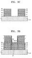
- a second surface emitting laser for emitting light having the second wavelength ⁇ 2 is formed in the removed area. That is, referring to Figure 3B, a first etching mask 61 having a predetermined pattern is disposed on the first upper reflector 45. Then, by performing etching, for example, by a dry etching method, parts of the first upper reflector 45, the first active layer 43, and the first lower reflector 41 located in a predetermined area are removed.
- a protection film 63 for enclosing the first surface emitting laser is formed.
- the protection film 63 is formed of silicon nitride or silicon oxide. The protection film 63 will be used to facilitate removal of an unnecessary portion growing on the upper surface of the first surface emitting laser when a second surface emitting laser is formed in a process which will be described later, and also to protect the first surface emitting laser having completed its growth in a subsequent process.
- the second surface emitting laser is formed on the substrate 30 and the protection film 63.
- the second surface emitting laser for emitting light having the second wavelength ⁇ 2 is formed by depositing the second lower reflector 51, the second active layer 53, and the second upper reflector 55 in order on the substrate 30.
- the second lower reflector 51 is formed by alternately depositing two semiconductor material layers with the same type of impurities, but different refractive indices
- the second upper reflector 55 is formed by alternately depositing two semiconductor material layers having different refractive indices and the opposite type of impurities to the second lower reflector 51.
- the second surface emitting laser is preferably grown by the epitaxial growth method with the same semiconductor equipment used for the first surface emitting laser.
- a second etching mask 67 is partially provided on of the upper surface of the second upper reflector 55, as shown in Figure 3D, so that the remaining portion except for part of the second surface emitting laser formed neighboring the first surface emitting laser can be removed.
- the remaining second surface emitting laser except for an area under the second etching mask 67 is removed by etching. Then, the protection layer 63 is removed.
- the first and second upper electrodes 47 and 57 on which the first and second windows 47a and 57a for emitting light are provided are formed on the upper surfaces of the first and second upper reflectors 45 and 55.
- the lower electrode 35 is formed on the bottom surface of the substrate 30 and thus the multi-wavelength surface emitting laser is completely manufactured.
- a step for partially forming the first and second high resistance portions 46 and 56 by the proton injection process or the oxidation process in each of the first and second upper reflectors 45 and 55 is performed before the first and second upper electrodes 47 and 57 are formed.
- the multi-wavelength surface emitting laser manufactured according to the preferred embodiment of the present invention since light having different wavelengths can be simultaneously emitted from a single substrate, optical alignment is easy compared to a method in which surface emitting lasers manufactured by an additional process are attached to a substrate. Also, since the first and second surface emitting lasers are manufactured in consecutive processes, the manufacturing process thereof is simple.
Landscapes
- Physics & Mathematics (AREA)
- Condensed Matter Physics & Semiconductors (AREA)
- General Physics & Mathematics (AREA)
- Electromagnetism (AREA)
- Optics & Photonics (AREA)
- Geometry (AREA)
- Semiconductor Lasers (AREA)
Abstract
Description
Claims (5)
- A multi-wavelength surface emitting laser for emitting light having a first wavelength and light having a second wavelength, the laser comprising:a substrate (30);a first surface emitting laser for emitting light having a first wavelength, directly formed on a portion of an upper surface of the substrate (30) and including a first lower reflector (41) formed by alternately depositing two semiconductor material layers with the same type of impurities, but different refractive indices, a first active layer (43), and a first upper reflector (45) formed by depositing two semiconductor material layers having different refractive indices and the opposite type of impurities to the first lower reflector (41);a second surface emitting laser for emitting light having a second wavelength, directly formed on a portion of an upper surface of the substrate (30) neighboring the first surface emitting laser and including a second lower reflector (51) formed by alternately depositing two semiconductor material layers having different refractive indices and the same type of impurities, a second active layer (53), and a second upper reflector (55) formed by depositing two semiconductor material layers having different refractive indices and the opposite type of impurities to the second lower reflector (51); anda lower electrode layer and first and second upper electrodes (47, 57) formed on one surface of the substrate (30) and the first and second upper reflectors (45, 55), respectively, for applying electric power.
- The laser as claimed in claim 1, further comprising first and second high resistance portions (46, 56) partially formed in the first and second upper reflectors (45, 55), respectively, for limiting a flow of current.
- A method for manufacturing a multi-wavelength surface emitting laser comprising the steps of:forming a first surface emitting laser for emitting light having a first wavelength by sequentially depositing on a prepared substrate (30) a first lower reflector (41) formed by alternately depositing two semiconductor material layers with the same type of impurities, but different refractive indices, a first active layer (43), and a first upper reflector (45) formed by alternately depositing two semiconductor material layers having the opposite type of impurities to the first lower reflector and different refractive indices;partially removing the first upper reflector (45), the first active layer (43), and the first lower reflection layer (41) by etching;forming a protection film (63) on the outer surface of the first surface emitting laser;forming a second surface emitting laser for emitting light having a second wavelength by sequentially depositing on the substrate (30) and the protection film (63) a second lower reflector (51) formed by alternately depositing two semiconductor material layers having the same type of impurities, but different refractive indices, a second active layer (53), and a second upper reflector (55) formed by alternately depositing two semiconductor material layers having the opposite type of impurities to the second lower reflector and different refractive indices;removing the second lower reflector (55), the second active layer (53), and the second upper reflection layer (51) formed on upper surface portions of the protection film by etching; andremoving remaining portions of the protection film (63) and forming first and second upper electrodes (47, 57) on upper surfaces of the first and second upper reflection layers (41, 51), respectively, and a lower electrode (35) on a bottom surface of the substrate (30).
- The method as claimed in claim 3, wherein the protection film (63) is formed of one selected from a group consisting of silicon nitride and silicon oxide.
- The method as claimed in claim 3, further comprising a step of forming first and second high resistance portions (46, 56) by injecting protons into part of the first and second upper reflectors (45, 55) before the first and second upper electrodes (47, 57) are formed.
Applications Claiming Priority (2)
| Application Number | Priority Date | Filing Date | Title |
|---|---|---|---|
| KR1020000041737A KR100727907B1 (en) | 2000-07-20 | 2000-07-20 | Multi-wavelength surface light laser and its manufacturing method |
| KR2000041737 | 2000-07-20 |
Publications (3)
| Publication Number | Publication Date |
|---|---|
| EP1182758A2 true EP1182758A2 (en) | 2002-02-27 |
| EP1182758A3 EP1182758A3 (en) | 2004-05-12 |
| EP1182758B1 EP1182758B1 (en) | 2007-01-24 |
Family
ID=19679055
Family Applications (1)
| Application Number | Title | Priority Date | Filing Date |
|---|---|---|---|
| EP01303025A Expired - Lifetime EP1182758B1 (en) | 2000-07-20 | 2001-03-30 | Multi-wavelength surface emitting laser and method for manufacturing the same |
Country Status (7)
| Country | Link |
|---|---|
| US (2) | US6778578B2 (en) |
| EP (1) | EP1182758B1 (en) |
| JP (1) | JP3464204B2 (en) |
| KR (1) | KR100727907B1 (en) |
| CN (1) | CN100403608C (en) |
| DE (1) | DE60126205T2 (en) |
| TW (1) | TW493304B (en) |
Cited By (3)
| Publication number | Priority date | Publication date | Assignee | Title |
|---|---|---|---|---|
| EP1531466A3 (en) * | 2003-11-17 | 2007-09-19 | Alps Electric Co., Ltd. | Wavelength-tunable light source |
| WO2014085562A1 (en) * | 2012-11-30 | 2014-06-05 | Corning Incorporated | Multiwavelength quantum cascade laser via growth of different active and passive cores |
| US9231368B2 (en) | 2012-11-30 | 2016-01-05 | Thorlabs Quantum Electronics, Inc. | Passive waveguide structure with alternating GaInAs/AlInAs layers for mid-infrared optoelectronic devices |
Families Citing this family (22)
| Publication number | Priority date | Publication date | Assignee | Title |
|---|---|---|---|---|
| US8129253B2 (en) * | 2001-08-13 | 2012-03-06 | Finisar Corporation | Providing current control over wafer borne semiconductor devices using trenches |
| JP4537658B2 (en) * | 2002-02-22 | 2010-09-01 | 株式会社リコー | Surface emitting laser element, surface emitting laser array using the surface emitting laser element, electrophotographic system, surface emitting laser module, optical communication system, optical interconnection system, and surface emitting laser element manufacturing method |
| US8205385B2 (en) * | 2003-06-20 | 2012-06-26 | Konvin Associates Ltd. | Dual panel system for controlling the passage of light through architectural structures |
| US7281353B2 (en) * | 2003-06-20 | 2007-10-16 | Konvin Associates Ltd. | Dual panel system for controlling the passage of light through architectural structures |
| US7218660B2 (en) * | 2003-10-27 | 2007-05-15 | Avago Technologies Fiber Ip (Singapore) Pte. Ltd. | Single-mode vertical cavity surface emitting lasers and methods of making the same |
| US7058106B2 (en) * | 2003-12-10 | 2006-06-06 | Widjaja Wilson H | Screenable moisture-passivated planar index-guided VCSEL |
| US7569860B2 (en) * | 2004-01-20 | 2009-08-04 | Binoptics Corporation | Integrated photonic devices |
| US7310358B2 (en) * | 2004-12-17 | 2007-12-18 | Palo Alto Research Center Incorporated | Semiconductor lasers |
| US7579204B2 (en) * | 2005-01-26 | 2009-08-25 | Sony Corporation | Method of production of semiconductor light emission device and method of production of light emission apparatus |
| JP2006313875A (en) * | 2005-04-08 | 2006-11-16 | Mitsubishi Electric Corp | Semiconductor laser device |
| US20060288645A1 (en) * | 2005-06-10 | 2006-12-28 | Cpi International Inc. | Method and apparatus for selective solar control |
| US20070163732A1 (en) * | 2006-01-13 | 2007-07-19 | Konvin Associates Ltd. | Method and device for controlling the passage of radiant energy into architectural structures |
| JP4985100B2 (en) * | 2007-05-28 | 2012-07-25 | ソニー株式会社 | Multi-wavelength laser, optical pickup device and optical disk device |
| US10868407B2 (en) * | 2015-06-04 | 2020-12-15 | Hewlett Packard Enterprise Development Lp | Monolithic WDM VCSELS with spatially varying gain peak and fabry perot wavelength |
| CN106887788B (en) * | 2017-04-27 | 2019-07-23 | 中国科学院长春光学精密机械与物理研究所 | A vertical cavity surface emitting laser and method of making the same |
| CN111435781B (en) * | 2019-01-15 | 2022-03-18 | 中国科学院半导体研究所 | Vertical Cavity Surface Emitting Semiconductor Laser Structure |
| EP3739700B8 (en) * | 2019-05-16 | 2021-09-29 | Changchun Institute of Optics, Fine Mechanics and Physics, Chinese Academy of Sciences | Vertical-cavity surface-emitting laser |
| US11936163B2 (en) | 2020-08-24 | 2024-03-19 | Changchun Institute Of Optics, Fine Mechanics And Physics | Radiation emitter |
| EP3961829B1 (en) | 2020-08-24 | 2023-10-04 | Changchun Institute of Optics, Fine Mechanics and Physics, Chinese Academy of Sciences | Radiation emitter |
| EP4007092B1 (en) * | 2020-11-30 | 2023-05-24 | Changchun Institute of Optics, Fine Mechanics and Physics, Chinese Academy of Sciences | Radiation emitter |
| CN116526301B (en) * | 2023-05-10 | 2026-03-17 | 江苏长光时空光电技术有限公司 | A surface-emitting laser semiconductor array chip and its fabrication method |
| CN121076583A (en) * | 2025-11-07 | 2025-12-05 | 长春理工大学 | Multi-wavelength quantum cascade laser driven by segmented voltage |
Family Cites Families (13)
| Publication number | Priority date | Publication date | Assignee | Title |
|---|---|---|---|---|
| JPS63227089A (en) * | 1987-03-17 | 1988-09-21 | Matsushita Electric Ind Co Ltd | Manufacture of multi-wavelength semiconductor laser |
| JPH042189A (en) * | 1990-04-18 | 1992-01-07 | Nec Corp | Surface emitting semiconductor laser |
| JPH06302901A (en) * | 1993-04-12 | 1994-10-28 | Nippon Telegr & Teleph Corp <Ntt> | Optical pulse generation control element |
| JPH07312462A (en) * | 1994-03-24 | 1995-11-28 | Mitsubishi Electric Corp | Method for manufacturing surface emitting laser diode and surface emitting laser diode |
| US5729563A (en) * | 1994-07-07 | 1998-03-17 | Hewlett-Packard Company | Method and apparatus for optically and thermally isolating surface emitting laser diodes |
| JPH09312462A (en) * | 1996-05-21 | 1997-12-02 | Kanegafuchi Chem Ind Co Ltd | Method of forming electric circuit |
| US5699375A (en) * | 1996-07-08 | 1997-12-16 | Xerox Corporation | Multiple wavelength, surface emitting laser with broad bandwidth distributed Bragg reflectors |
| JPH10233559A (en) * | 1997-02-20 | 1998-09-02 | Canon Inc | Semiconductor laser device, manufacturing method thereof, and optical communication system using the same |
| JPH10270799A (en) * | 1997-03-21 | 1998-10-09 | Sanyo Electric Co Ltd | Light emitting element |
| US6021146A (en) * | 1997-09-15 | 2000-02-01 | Motorola, Inc. | Vertical cavity surface emitting laser for high power single mode operation and method of fabrication |
| JP2000011417A (en) * | 1998-06-26 | 2000-01-14 | Toshiba Corp | Semiconductor laser array and manufacturing method thereof, optical integrated unit, optical pickup, and optical disk drive |
| US6560262B1 (en) * | 1999-01-26 | 2003-05-06 | Triquint Technology Holding Co. | Vertical cavity surface emitting laser array and a process for making same |
| US6546035B2 (en) * | 2000-02-29 | 2003-04-08 | Matsushita Electric Industrial Co., Ltd. | Semiconductor laser diode array and method of fabricating the same |
-
2000
- 2000-07-20 KR KR1020000041737A patent/KR100727907B1/en not_active Expired - Fee Related
-
2001
- 2001-03-08 TW TW090105479A patent/TW493304B/en not_active IP Right Cessation
- 2001-03-14 JP JP2001072603A patent/JP3464204B2/en not_active Expired - Fee Related
- 2001-03-28 CN CNB011121106A patent/CN100403608C/en not_active Expired - Fee Related
- 2001-03-30 DE DE60126205T patent/DE60126205T2/en not_active Expired - Fee Related
- 2001-03-30 EP EP01303025A patent/EP1182758B1/en not_active Expired - Lifetime
- 2001-04-17 US US09/835,319 patent/US6778578B2/en not_active Expired - Fee Related
-
2004
- 2004-07-14 US US10/890,289 patent/US7387906B2/en not_active Expired - Fee Related
Cited By (7)
| Publication number | Priority date | Publication date | Assignee | Title |
|---|---|---|---|---|
| EP1531466A3 (en) * | 2003-11-17 | 2007-09-19 | Alps Electric Co., Ltd. | Wavelength-tunable light source |
| WO2014085562A1 (en) * | 2012-11-30 | 2014-06-05 | Corning Incorporated | Multiwavelength quantum cascade laser via growth of different active and passive cores |
| US9231368B2 (en) | 2012-11-30 | 2016-01-05 | Thorlabs Quantum Electronics, Inc. | Passive waveguide structure with alternating GaInAs/AlInAs layers for mid-infrared optoelectronic devices |
| US9601901B2 (en) | 2012-11-30 | 2017-03-21 | Thorlabs Quantum Electronics, Inc. | Passive waveguide structure with alternating GaInAs/AlInAs layers for mid-infrared optoelectronic devices |
| US9685766B2 (en) | 2012-11-30 | 2017-06-20 | Thorlabs Quantum Electronics, Inc. | Multiwavelength quantum cascade laser via growth of different active and passive cores |
| US20170179685A1 (en) * | 2012-11-30 | 2017-06-22 | Thorlabs Quantum Electronics, Inc. | Multiwavelength quantum cascade laser via growth of different active and passive cores |
| US10431957B2 (en) | 2012-11-30 | 2019-10-01 | Thorlabs Quantum Electronics, Inc. | Multiwavelength quantum cascade laser via growth of different active and passive cores |
Also Published As
| Publication number | Publication date |
|---|---|
| CN100403608C (en) | 2008-07-16 |
| US20040258121A1 (en) | 2004-12-23 |
| TW493304B (en) | 2002-07-01 |
| JP2002043693A (en) | 2002-02-08 |
| US20020021733A1 (en) | 2002-02-21 |
| US6778578B2 (en) | 2004-08-17 |
| US7387906B2 (en) | 2008-06-17 |
| DE60126205T2 (en) | 2007-10-11 |
| CN1335658A (en) | 2002-02-13 |
| DE60126205D1 (en) | 2007-03-15 |
| KR20020008508A (en) | 2002-01-31 |
| KR100727907B1 (en) | 2007-06-14 |
| JP3464204B2 (en) | 2003-11-05 |
| EP1182758A3 (en) | 2004-05-12 |
| EP1182758B1 (en) | 2007-01-24 |
Similar Documents
| Publication | Publication Date | Title |
|---|---|---|
| EP1182758A2 (en) | Multi-wavelength surface emitting laser and method for manufacturing the same | |
| KR102518449B1 (en) | Indium Phosphide VCSEL with Dielectric DBR | |
| KR0147857B1 (en) | Optical devices with electron-beam evaporated multilayer mirror | |
| US7288421B2 (en) | Method for forming an optoelectronic device having an isolation layer | |
| US20050063440A1 (en) | Epitaxial mode-confined vertical cavity surface emitting laser (VCSEL) and method of manufacturing same | |
| EP1217702A2 (en) | Semiconductor light-emitting device with improved electro-optical characteristics and method of manufacturing the same | |
| JPH10107389A (en) | Method of manufacturing semiconductor optoelectronic device, device and device matrix manufactured by this method | |
| TW200828707A (en) | Multiwavelength semiconductor laser array and method of manufacturing the same | |
| JP2001237497A (en) | Passive semiconductor structure and manufacturing method therefor | |
| KR101300355B1 (en) | Vcsel system with transverse p/n junction | |
| JP3219823B2 (en) | Semiconductor light emitting device | |
| US7095771B2 (en) | Implant damaged oxide insulating region in vertical cavity surface emitting laser | |
| KR20040010719A (en) | Method and apparatus for producing vcsels with dielectric mirrors and self-aligned gain guide | |
| US5563900A (en) | Broad spectrum surface-emitting led | |
| KR100754156B1 (en) | Multi-wavelength surface light laser and its manufacturing method | |
| US20080247437A1 (en) | Tunable long-wavelength vcsel system | |
| JP4909262B2 (en) | Optical pumping semiconductor device | |
| JP2007059909A (en) | Semiconductor system having ring laser manufactured by epitaxial layer growth | |
| KR20050001858A (en) | Low loss vertical-cavity surface-emitting laser and fabricating method the same | |
| CN113422292B (en) | Vertical cavity surface emitting laser and manufacturing method and application thereof | |
| KR100269145B1 (en) | Surface emitting laser diode and method for manufacturing it | |
| JP4178901B2 (en) | Semiconductor optical device and method of manufacturing semiconductor optical device | |
| CN121355694A (en) | A vertical-cavity surface-emitting laser and its fabrication method | |
| JPH0595157A (en) | Semiconductor laser device |
Legal Events
| Date | Code | Title | Description |
|---|---|---|---|
| PUAI | Public reference made under article 153(3) epc to a published international application that has entered the european phase |
Free format text: ORIGINAL CODE: 0009012 |
|
| 17P | Request for examination filed |
Effective date: 20010418 |
|
| AK | Designated contracting states |
Kind code of ref document: A2 Designated state(s): AT BE CH CY DE DK ES FI FR GB GR IE IT LI LU MC NL PT SE TR |
|
| AX | Request for extension of the european patent |
Free format text: AL;LT;LV;MK;RO;SI |
|
| PUAL | Search report despatched |
Free format text: ORIGINAL CODE: 0009013 |
|
| AK | Designated contracting states |
Kind code of ref document: A3 Designated state(s): AT BE CH CY DE DK ES FI FR GB GR IE IT LI LU MC NL PT SE TR |
|
| AX | Request for extension of the european patent |
Extension state: AL LT LV MK RO SI |
|
| AKX | Designation fees paid |
Designated state(s): DE FR GB |
|
| 17Q | First examination report despatched |
Effective date: 20050204 |
|
| GRAP | Despatch of communication of intention to grant a patent |
Free format text: ORIGINAL CODE: EPIDOSNIGR1 |
|
| RIN1 | Information on inventor provided before grant (corrected) |
Inventor name: CHUNG, MIN-HYUNG Inventor name: LEE, EUN-KYUNG |
|
| GRAS | Grant fee paid |
Free format text: ORIGINAL CODE: EPIDOSNIGR3 |
|
| GRAA | (expected) grant |
Free format text: ORIGINAL CODE: 0009210 |
|
| AK | Designated contracting states |
Kind code of ref document: B1 Designated state(s): DE FR GB |
|
| REG | Reference to a national code |
Ref country code: GB Ref legal event code: FG4D |
|
| REF | Corresponds to: |
Ref document number: 60126205 Country of ref document: DE Date of ref document: 20070315 Kind code of ref document: P |
|
| ET | Fr: translation filed | ||
| PLBE | No opposition filed within time limit |
Free format text: ORIGINAL CODE: 0009261 |
|
| STAA | Information on the status of an ep patent application or granted ep patent |
Free format text: STATUS: NO OPPOSITION FILED WITHIN TIME LIMIT |
|
| 26N | No opposition filed |
Effective date: 20071025 |
|
| PGFP | Annual fee paid to national office [announced via postgrant information from national office to epo] |
Ref country code: DE Payment date: 20080407 Year of fee payment: 8 Ref country code: FR Payment date: 20080311 Year of fee payment: 8 |
|
| PGFP | Annual fee paid to national office [announced via postgrant information from national office to epo] |
Ref country code: GB Payment date: 20080402 Year of fee payment: 8 |
|
| GBPC | Gb: european patent ceased through non-payment of renewal fee |
Effective date: 20090330 |
|
| REG | Reference to a national code |
Ref country code: FR Ref legal event code: ST Effective date: 20091130 |
|
| PG25 | Lapsed in a contracting state [announced via postgrant information from national office to epo] |
Ref country code: DE Free format text: LAPSE BECAUSE OF NON-PAYMENT OF DUE FEES Effective date: 20091001 |
|
| PG25 | Lapsed in a contracting state [announced via postgrant information from national office to epo] |
Ref country code: FR Free format text: LAPSE BECAUSE OF NON-PAYMENT OF DUE FEES Effective date: 20091123 Ref country code: GB Free format text: LAPSE BECAUSE OF NON-PAYMENT OF DUE FEES Effective date: 20090330 |