EP1182703A2 - Semiconductor device having integrated capacitor and/or inductor - Google Patents
Semiconductor device having integrated capacitor and/or inductor Download PDFInfo
- Publication number
- EP1182703A2 EP1182703A2 EP01119376A EP01119376A EP1182703A2 EP 1182703 A2 EP1182703 A2 EP 1182703A2 EP 01119376 A EP01119376 A EP 01119376A EP 01119376 A EP01119376 A EP 01119376A EP 1182703 A2 EP1182703 A2 EP 1182703A2
- Authority
- EP
- European Patent Office
- Prior art keywords
- forming
- semiconductor device
- conductive layer
- thin film
- passive element
- Prior art date
- Legal status (The legal status is an assumption and is not a legal conclusion. Google has not performed a legal analysis and makes no representation as to the accuracy of the status listed.)
- Granted
Links
Images















Classifications
-
- H—ELECTRICITY
- H10—SEMICONDUCTOR DEVICES; ELECTRIC SOLID-STATE DEVICES NOT OTHERWISE PROVIDED FOR
- H10W—GENERIC PACKAGES, INTERCONNECTIONS, CONNECTORS OR OTHER CONSTRUCTIONAL DETAILS OF DEVICES COVERED BY CLASS H10
- H10W72/00—Interconnections or connectors in packages
-
- H—ELECTRICITY
- H10—SEMICONDUCTOR DEVICES; ELECTRIC SOLID-STATE DEVICES NOT OTHERWISE PROVIDED FOR
- H10W—GENERIC PACKAGES, INTERCONNECTIONS, CONNECTORS OR OTHER CONSTRUCTIONAL DETAILS OF DEVICES COVERED BY CLASS H10
- H10W20/00—Interconnections in chips, wafers or substrates
- H10W20/40—Interconnections external to wafers or substrates, e.g. back-end-of-line [BEOL] metallisations or vias connecting to gate electrodes
- H10W20/497—Inductive arrangements or effects of, or between, wiring layers
-
- H—ELECTRICITY
- H10—SEMICONDUCTOR DEVICES; ELECTRIC SOLID-STATE DEVICES NOT OTHERWISE PROVIDED FOR
- H10D—INORGANIC ELECTRIC SEMICONDUCTOR DEVICES
- H10D84/00—Integrated devices formed in or on semiconductor substrates that comprise only semiconducting layers, e.g. on Si wafers or on GaAs-on-Si wafers
-
- H—ELECTRICITY
- H10—SEMICONDUCTOR DEVICES; ELECTRIC SOLID-STATE DEVICES NOT OTHERWISE PROVIDED FOR
- H10D—INORGANIC ELECTRIC SEMICONDUCTOR DEVICES
- H10D84/00—Integrated devices formed in or on semiconductor substrates that comprise only semiconducting layers, e.g. on Si wafers or on GaAs-on-Si wafers
- H10D84/201—Integrated devices formed in or on semiconductor substrates that comprise only semiconducting layers, e.g. on Si wafers or on GaAs-on-Si wafers characterised by the integration of only components covered by H10D1/00 or H10D8/00, e.g. RLC circuits
- H10D84/204—Integrated devices formed in or on semiconductor substrates that comprise only semiconducting layers, e.g. on Si wafers or on GaAs-on-Si wafers characterised by the integration of only components covered by H10D1/00 or H10D8/00, e.g. RLC circuits of combinations of diodes or capacitors or resistors
- H10D84/212—Integrated devices formed in or on semiconductor substrates that comprise only semiconducting layers, e.g. on Si wafers or on GaAs-on-Si wafers characterised by the integration of only components covered by H10D1/00 or H10D8/00, e.g. RLC circuits of combinations of diodes or capacitors or resistors of only capacitors
-
- H—ELECTRICITY
- H10—SEMICONDUCTOR DEVICES; ELECTRIC SOLID-STATE DEVICES NOT OTHERWISE PROVIDED FOR
- H10W—GENERIC PACKAGES, INTERCONNECTIONS, CONNECTORS OR OTHER CONSTRUCTIONAL DETAILS OF DEVICES COVERED BY CLASS H10
- H10W20/00—Interconnections in chips, wafers or substrates
- H10W20/40—Interconnections external to wafers or substrates, e.g. back-end-of-line [BEOL] metallisations or vias connecting to gate electrodes
- H10W20/495—Capacitive arrangements or effects of, or between wiring layers
- H10W20/496—Capacitor integral with wiring layers
-
- H—ELECTRICITY
- H10—SEMICONDUCTOR DEVICES; ELECTRIC SOLID-STATE DEVICES NOT OTHERWISE PROVIDED FOR
- H10W—GENERIC PACKAGES, INTERCONNECTIONS, CONNECTORS OR OTHER CONSTRUCTIONAL DETAILS OF DEVICES COVERED BY CLASS H10
- H10W74/00—Encapsulations, e.g. protective coatings
- H10W74/10—Encapsulations, e.g. protective coatings characterised by their shape or disposition
- H10W74/111—Encapsulations, e.g. protective coatings characterised by their shape or disposition the semiconductor body being completely enclosed
- H10W74/129—Encapsulations, e.g. protective coatings characterised by their shape or disposition the semiconductor body being completely enclosed forming a chip-scale package [CSP]
-
- H—ELECTRICITY
- H10—SEMICONDUCTOR DEVICES; ELECTRIC SOLID-STATE DEVICES NOT OTHERWISE PROVIDED FOR
- H10D—INORGANIC ELECTRIC SEMICONDUCTOR DEVICES
- H10D1/00—Resistors, capacitors or inductors
- H10D1/40—Resistors
- H10D1/47—Resistors having no potential barriers
-
- H—ELECTRICITY
- H10—SEMICONDUCTOR DEVICES; ELECTRIC SOLID-STATE DEVICES NOT OTHERWISE PROVIDED FOR
- H10D—INORGANIC ELECTRIC SEMICONDUCTOR DEVICES
- H10D1/00—Resistors, capacitors or inductors
- H10D1/60—Capacitors
- H10D1/68—Capacitors having no potential barriers
Definitions
- the present invention relates to a semiconductor device of a CSP (Chip Size Package) structure and a method of manufacturing the same.
- CSP Chip Size Package
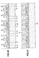
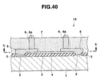
- FIG. 40 is a cross sectional view exemplifying the construction of a semiconductor device 10 of a CSP structure
- FIG. 41 is a cross sectional view along the line V-V shown in FIG. 40 showing the construction of the semiconductor device excluding a conductor layer 5.
- the semiconductor device 10 comprises a plurality of connection pads 2 formed of aluminum electrodes or the like and formed on the front side (circuit side) of a semiconductor substrate 1.
- a passivation film 3 consisting of silicon oxide, silicon nitride or the like is formed on the side of the upper surfaces of the substrate 1 and the connection pads 2 in a manner to expose the central portion of each of the connection pads 2.
- a circuit element-forming region DA is formed on the front surface of the semiconductor substrate 1 except the forming region of the connection pads 2, and circuit elements are formed in an integrated manner within the circuit element-forming region DA.
- a protective film 4 is formed on the passivation film 3 in a manner to form an open portion in the central portion of each connection pad 2.
- the entire surface on the side of the circuit of the semiconductor substrate 1 is coated with, for example, a polyimide series resin material, followed by curing the coated resin material. Then, a resist patterning and a protective film patterning are applied by using an etching solution, followed by peeling off the resist film so as to form the protective film 4.
- Conductive layers 5 each electrically connected to the connection pad 2 are formed on the protective film 4, a plurality of posts 6 for connection to the external circuit, which are columnar electrodes are formed in predetermined positions on the conductor layers 5.
- a metallizing treatment such as a solder printing is applied to the tip of the post 6 so as to form a metallized projecting edge surface 6a that is to be connected to a terminal (not shown) on the circuit substrate.
- the post 6 is formed straight in a height of at least 50 ⁇ m and typically about 100 to 150 ⁇ m so as to absorb the stress generated by the difference in the thermal expansion coefficient between the semiconductor substrate 1 and the circuit substrate.
- a sealing film 7 made of a resin material such as a polyimide resin or an epoxy resin is formed on that portion of the entire circuit surface of the semiconductor substrate 1 which is positioned between the adjacent posts 6.
- a native oxide film is removed from the projecting edge surface 6a of the post 6, followed by applying a metallizing treatment such as a solder printing to the projecting edge surface 6a so as to form a terminal portion for connection to the external circuit.
- the terminal portion of the post 6 for the connection to the external circuit is arranged to face the terminal of the circuit substrate and bonded by, for example, a soldering to the terminal of the circuit substrate so as to achieve the mounting of the semiconductor device to the circuit substrate.
- a transceiver chip equipped with a wireless I/F function such as Bluetooth
- the semiconductor chip it is absolutely necessary for the semiconductor chip to be equipped with an RF functional elements such as a PLL circuit, a VCO circuit or a filter circuit.
- an RF functional elements such as a PLL circuit, a VCO circuit or a filter circuit.
- various passive elements such as a capacitance element and an inductance element in the circuit element-forming region DA of the semiconductor substrate 1.
- the formation of these passive elements necessitates a relatively large area, with the result that, if these passive elements are to be formed in the circuit element-forming region DA, the chip area is unavoidably increased. If the chip area is increased in the semiconductor device 10 of the CSP structure described above, various problems are generated. For example, it is impossible to increase the mounting density on the circuit substrate. Also, the number of chips that can be obtained from a single semiconductor wafer is decreased so as to lower the yield of manufacture and to increase the manufacturing cost.
- the various passive elements for realizing the RF functional elements are formed as discrete parts and mounted on the outside of the chip.
- An object of the present invention is to provide a semiconductor device capable of mounting passive elements on a chip without inviting the increase in the chip area and a method of manufacturing the particular semiconductor device.
- a semiconductor device comprising a semiconductor substrate having a circuit element-forming region and a plurality of connection pads formed therein; an insulating film formed on the circuit element-forming region; and at least one thin film passive element including a columnar electrode for connection to the external circuit connected to at least one of a plurality of connection pads and at least one capacitance element consisting of a plurality of conductive layers and dielectric material layers and an inductance element consisting of a conductive film patterned in the shape of generating an inductance component, the capacitance element and the inductance element being formed on the insulating film on the circuit element region.
- the thin film passive element it is possible for the thin film passive element to be arranged in various types on the circuit element-forming region DA so as to be connected to the circuit element of the circuit element-forming region DA through the connection pads or so as to be connected to the external connection terminals through the columnar electrodes. As a result, it is possible to mount the thin film passive elements in a stacked fashion without inviting an increase in the chip area. Also, the passive elements, which were required to be mounted outside the chip as discrete parts, can be mounted within the chip so as to decrease the module size.
- a method of manufacturing a semiconductor device of the particular construction described above In the manufacturing method of the present invention, a semiconductor wafer having a plurality of chip forming regions is prepared first. A connection pad is formed in each of the chip forming regions. After a passivation film exposing the central portion of each connection pad is formed on the upper surfaces of the connection pads formed in the chip forming regions, a first protective film is formed on the upper surface of the passivation film.
- a capacitance element is formed as the thin film passive element
- a first conductive layer connected to the connection pad is formed on the first protective film
- a dielectric material layer is formed on that portion of the first conductive film in which the capacitance element is formed, followed by forming a second conductive film on the dielectric material layer so as to form the capacitance element.
- an inductance element as the thin film passive element
- a first conductive layer connected to a connection pad is formed on the first protective layer, and a conductive layer patterned in a shape adapted for generating an inductance component such as an angular eddy shape or a loop shape is formed so as to form the inductance element.
- a magnetic film on the conductive layer forming the inductance element with the protective film interposed therebetween. In this case, it is possible to increase the inductance value of an inductance element.
- dicing is applied to each chip forming region so as to separate the semiconductor water into individual semiconductor devices, thereby forming a plurality of semiconductor devices of the present invention each having at least one thin film passive element.
- dicing is applied to each chip forming region so as to separate the semiconductor water into individual semiconductor devices, thereby forming a plurality of semiconductor devices of the present invention each having at least one thin film passive element.
- FIG. 1 is a cross sectional view showing a semiconductor device 200 according to a first embodiment of the present invention. Also, FIGS. 2A and 2B show the gist portions of the semiconductor device in the cross section along the line I-I shown in FIG. 1 except a sealing film 17.
- the semiconductor device 200 comprises a plurality of connection pads 12 consisting of, for example, aluminum electrodes formed to surround a circuit element-forming region DA on the front side (circuit side) of a semiconductor substrate 11, a passivation film 13 consisting of silicon oxide or silicon nitride and formed on the side of the upper surface of the connection pads 12 in a manner to expose the central portion of each of the connection pads 12, and a protective film 14 formed on the upper surface of the passivation film 13, hereinafter referred to as a first protective film 14, like the conventional semiconductor device 10 shown in FIGS. 40 and 41.
- a conductive layer 15 (hereinafter referred to as first conductive layer 15) connected to the connection pad 12 is formed on the first protective film 14.
- the semiconductor device 200 according to the first embodiment of the present invention also comprises a plurality of conductive layers 20, hereinafter referred to as second conductive layers 20, formed above the first conductive layers 15 and a plurality of dielectric material layers 18 interposed between the first conductive layers 15 and the second conductive layers 20.
- the semiconductor device 200 according to the first embodiment of the present invention is featured in that these first and second conductive layers 15, 20 and the dielectric material layers 18 interposed between the first and second conductive layers 15 and 20 collectively form capacitance elements C providing a plurality of thin film passive elements.
- the thin film passive element represents a passive element formed on the first protective layer 14 and including at least one conductive layer in the form of a thin film.
- the thin film passive element represents a capacitance element in the first embodiment of the present invention and in the second to third embodiments described herein later and an inductance element in each of the fourth to sixth embodiments of the present invention described herein later.
- the thin film passive element is combined with, for example, a circuit element in the circuit element-forming region DA so as to constitute a wireless I/F function.
- the thin film passive element in the present invention is not limited to those exemplified above and includes, for example, a thin film transformer, a thin film SAM (Surface Acoustic Wave) filter, a micro strip line, and an MMIC (Microwave Monolithic Integrated Circuit).
- a plurality of straight-shaped posts 16 or columnar electrodes for connection to the external circuit are formed in predetermined positions on the conductive layers 20.
- the post 16 is formed in a height of at least 50 ⁇ m and typically about 100 to 150 ⁇ m.
- a protective film 19, hereinafter referred to as a second protective film 19, is formed to surround the capacitance element C so as to electrically insulate the capacitance element C from the other members of the semiconductor device.
- the post 16 is formed on the first conductive layer 15 with the second conductive layer 20 interposed therebetween.
- the sealing film 17 consisting of a resin material such as a polyimide resin or an epoxy resin is formed between the adjacent posts 16, and an oxide film is removed from the edge surface 16a of the post 16 and a metallizing treatment such as a solder printing is applied to the exposed edge surface 16a so as to form a terminal portion for connection to the external circuit.
- a resin material such as a polyimide resin or an epoxy resin
- the capacitance value of the capacitance element C formed by the resultant structure is determined by the relative dielectric constant, thickness and area of the dielectric material forming the dielectric material layer 18.
- the dielectric material forming the dielectric material layer 18 includes, for example, barium titanate and tantalum titanate.
- the capacitance element C formed in the circuit element-forming region DA of the semiconductor substrate 11 by the construction described above can be arranged in various modes, as required. For example, as shown in FIG. 2A, it is possible to increase the area of the single dielectric material layer 18 so as to form the capacitance element C of a large capacitance as shown in FIG. 2A. Alternatively, it is also possible to arrange a plurality of capacitance elements C on the semiconductor substrate 11, as shown in FIG. 2B.
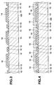
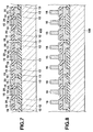
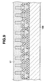
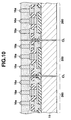
- FIGS. 3 to 10 are cross sectional views collectively showing a method of manufacturing the semiconductor device 200 according to the first embodiment of the present invention. The manufacturing method of the semiconductor device 200 will now be described with reference to these drawings.
- a wiring layer, a capacitance element, an inductance element, etc. are formed on a semiconductor wafer 100, followed by finally dividing the semiconductor wafer 100 for each chip so as to form the semiconductor substrate 11, thereby manufacturing the semiconductor device 200, as described herein later.
- a passivation film 13 consisting of, for example, silicon oxide or silicon nitride is formed first on the side of the upper surfaces of a plurality of connection pads 12 consisting of, for example, aluminum electrodes formed in the chip-forming regions on the circuit side of the semiconductor wafer 100, as shown in FIG. 3. Then, a first protective film 14 is formed on the upper surface of the passivation film 13 in a manner to form an opening in the central portion of each of the connection pads 12.
- the first protective film 14 is formed by, for example, coating the entire surface on the side of the circuit of the semiconductor wafer 100 with a polyimide series resin material and curing the coated resin material, followed by applying a resist patterning and a protective film patterning by using an etching solution and subsequently peeling off the resist. It is also possible to employ a printing method using a squeegee or a coating method utilizing an ink ejection from a nozzle for forming the first protective film 14. Also, the material of the protective film is not limited to the polyimide series resin material. Specifically, an epoxy series resin material, PBO (benzaoxidole series), etc. can also be used as the material of the protective film.
- a first conductive layer 15 is formed on the connection pads 12 exposed via the open portions formed in the first protective film 14 and the first protective films 14, as shown in FIG. 4.
- a UBM (under bump metal) layer (not shown) is deposited by, for example, a sputtering method on the entire surface of the first protective film 14 including the exposed surfaces of the connection pads 12, followed by coating and curing a photoresist film for an conductive layer.
- the cured photoresist film is patterned by a photolithography technology to form openings of a predetermined shape, followed by applying an electroplating to the portion opened by the resist, thereby forming the first conductive layer 15.
- the wiring material used for forming the conductive layer includes, for example, copper, aluminum and gold having good conductive properties.
- a dielectric material layer 18 is formed in a capacitance element-forming region on the first conductive layer 15, as shown in FIG. 5.
- the dielectric material layer 18 can be formed by, for example, forming a resist pattern, followed by depositing a dielectric material layer in a predetermined thickness by a sputtering method.
- a second protective film 19 serving to electrically isolating the dielectric material layer from the other layers is formed, followed by patterning the second conductive layer 19 to form openings in the portion where a second conductive layer 20 is to be formed and the portion where to the cutting for the dicing is applied, as shown in FIG. 6.
- the second protective film 19 can be formed as in the formation of the first protective layer 14. Specifically, after the entire surface on the side of the circuit of the semiconductor wafer 100 is coated with, for example, a polyimide series resin material and the resin material coating is cured, a resist patterning and a protective film patterning are applied to the cured resin material by using an etching solution and subsequently peeling off the resist layer.
- the second conductive layer 20 is formed so as to form a conductive portion electrically connected to the first conductive layer 15 exposed via the opening formed in the second protective film 19 and also electrically connected to the dielectric material layer 18 formed on the upper surface of the first conductive layer 15 so as to form a conductive layer portion forming a capacitance element, as shown in FIG. 7.
- the second conductive layer 20 can be formed by forming a resist pattern first, followed by applying an electroplating as in the formation of the first conductive layer 15.
- a plurality of posts 16 or columnar electrodes are formed in predetermined positions on the conductive layers 20, as shown in FIG. 8.
- the posts 16 can be formed as in the conventional method. Specifically, a photoresist for forming the posts is coated in a thickness of about, for example, at least 50 ⁇ m, and typically 100 to 150 ⁇ m and, then, the coated photoresist is cured, followed by forming openings exposing predetermined positions of the second conductive layer 20 and subsequently applying an electroplating to the openings thus formed. It is also possible to employ an electroless plating or a stud bump method for forming the posts 16.
- the materials used for forming the posts 16 include, for example, copper, solder, gold and nickel having good conductive properties.
- solder is used as a material for forming the post 16
- a printing method in addition to the methods pointed out above.
- a sealing film 17 is formed on the entire front surface on the front side (circuit side) of the semiconductor wafer 100 in a manner to cover the posts 16 by, for example, a molding method by using a resin material such as a polyimide resin or an epoxy resin, as shown in FIG. 9. It is desirable to form the sealing film 17 by using a resin material substantially equal in the main component to the resin material used for forming the first protective film 14 and the second protective film 19 in order to ensure a reliability relative to the change in the environment. Incidentally, it is also possible to employ, for example, a printing method, an immersion method, a spin coating method and a die coating method for forming the sealing film 17.
- the upper surface of the sealing film 17 is polished and cut so as to expose the edge surface 16a of the post 16, followed by removing an oxide film from the surface of the edge surface 16a and applying a metallizing treatment such as a solder printing treatment to the edge surface 16a of the post 16, as shown in FIG. 10.
- a dicing is applied along predetermined cut lines CL corresponding to the chip-forming regions so as to divide the semiconductor wafer 100 into the individual chip-forming regions and, thus, to form the individual semiconductor substrates 11, thereby forming the semiconductor device 200 shown in FIG. 1.
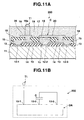
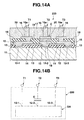
- FIGS. 11A to 15A are cross sectional views showing the connection modes of the capacitance elements C in accordance with the modes of arrangement of the second conductive layer 20 and the posts 16 in the semiconductor device 200, and FIGS. 11B to 15B show the corresponding equivalent circuit diagrams.
- FIG. 11A shows the first connection mode of the capacitance element in the first embodiment of the present invention, covering the case where the dielectric material layer 18 is formed on the first conductive layer 15 connected to the connection pad 12-2, and the second conductive layer 20 is stacked via the first conductive layer 15 connected to the connection pad 12-3 so as to form the capacitance element C, and the post 16 is not formed on the second conductive layer 20 forming a capacitance element.
- the second conductive layer 20 is formed in direct contact with the first conductive layer 15 not involved in the formation of the capacitance element, and the post 16 is formed on the second conductive layer 20 so as to be connected to an external connection terminal T1.
- both ends of the capacitance element C are connected to only the circuit element in the circuit element-forming region DA, as shown in FIG. 11B.
- FIG. 12A shows a second connection mode of the capacitance element in the first embodiment of the present invention, covering the case where the dielectric material layer 18 is formed on each of the first conductive layers 15 connected to the connection pads 12-1 and 12-2 and the second conductive layer 20 is stacked on each of these dielectric material layers 18 so as to form the capacitance element C, and the post 16 is formed on each of the second conductive layers 20 so as to be connected to each of the external connection terminals T1 and T2.
- the second conductive layer 20 is formed in direct contact with the first conductive layer 15 not involved in the formation of the capacitance element so as to be connected to an external connection terminal T3.
- each of the capacitance elements C is connected to the circuit element in the circuit element-forming region DA, and the other ends of these capacitance elements C are connected to the external connection terminals T1 and T2, as shown in FIG. 12B.
- FIG. 13A shows a third connection mode of the capacitance element in the first embodiment of the present invention, covering the case where the dielectric material layers 18 are formed in two points on the first conductive layer 15 connected to the connection pad 12-3 and the second conductive layers 20 are stacked on these dielectric layers 18 so as to form two capacitance elements C arranged in parallel, and the post 16 is formed on each of the second conductive layers 20 is formed so as to be connected to the external connection terminals T2 and T3.
- the post 16 is formed on the first conductive layer 15 not involved in the formation of the capacitance element via the second conductive layer 20 formed in direct contact with the first conductive layer 15 so as to be connected to the external connection terminal T1.
- each of the two capacitance elements C is commonly connected to the circuit element in the circuit element-forming region DA, and the other ends of these capacitance elements C are connected to the external connection terminals T2 and T3, as shown in FIG. 13B.
- FIG. 14A shows a fourth connection mode of the capacitance element in the first embodiment of the present invention, and covers the case where the dielectric material layer 18 is formed on the first conductive layer 15 connected to the connection pad 12-2 and the second conductive layer 20 is stacked on the dielectric material layer 18 so as to form the capacitance element C, and the post 16 is formed on the second conductive layer 20 so as to be connected to the external connection terminal T2.
- the posts 16 are formed on the first conductive layers 15, which are not involved in the formation of the capacitance element, with the second conductive layers 20 interposed therebetween, so as to be connected to the external connection terminals T1 and T2.
- one end of the capacitance element C is connected to the circuit element of the circuit element-forming region DA, with the other end being connected to the external connection terminal T2, as shown in FIG. 14B.
- FIG. 15A shows a fifth connection mode of the capacitance element in the first embodiment of the present invention, and covers the case where the dielectric material layer 18 is formed on the first conductive material layer 15 connected to the connection pad 12-2 and the second conductive layer 20, which is connected to the connection pad 12-3 via the first conductive layer 15, is stacked on the dielectric material layer 18 so as to form the capacitance element C, and the post 16 is formed on the second conductive layer 20 so as to be connected to the external connection terminal T3.
- the post 16 is formed on the first conductive layer 15, which is not involved in the formation of the capacitance element C, with the second conductive layer 20 interposed therebetween so as to be connected to the external connection terminal T1.
- one end of the capacitance element C is connected to the circuit element included in the circuit element-forming region DA and the other end of the capacitance element C is also connected to the circuit element of the circuit element-forming region DA and to the external connection terminal T3, as shown in FIG. 15B.
- the capacitance element C is formed in the circuit element-forming region DA so as to form the capacitance element C in a three dimensional direction and to be capable of connection to the circuit element, making it possible to mount the capacitance element without inviting an increase in the chip area. It follows that it is possible to diminish the chip area.
- the particular construction of the present invention contributes to the miniaturization of the module size because the capacitance element, which was required to be mounted outside the chip in the past, can be mounted within the chip.
- the dielectric material layer 18 is of a single layer structure.
- a ground layer made of the material equal to that of the first conductive layer 15 or the second conductive layer 20 in a position in the vicinity of the plane flush with the first conductive layer 15 or the second conductive layer 20.
- the dielectric material layer 18 is formed on the first conductive layer 15 for forming the capacitance element.
- the dielectric material in, for example, the second protective film 19 it is possible to mix the dielectric material in, for example, the second protective film 19 to allow the second protective film 19 to also perform the function of the dielectric material layer 18.
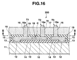
- FIG. 16 is a cross sectional view showing a semiconductor device 200 according to a second embodiment of the present invention
- FIGS. 17A and 17B are cross sectional views along the line II-II shown in FIG. 16 showing the gist portions of the semiconductor device 200 excluding the sealing film 17.
- FIGS. 18 and 19 are cross sectional views showing the construction and the manufacturing process of the semiconductor device 200 according to the second embodiment of the present invention.
- the members of the semiconductor device common with those of the semiconductor device according to the first embodiment of the present invention described above are denoted by the same reference numerals so as to avoid the overlapping description.
- the conductive layers 15 are arranged a predetermined distance apart from each other on the first protective layer 14, and the dielectric material layer 18 is formed in the clearance between adjacent conductive layers 15 in a manner to abut against the edge surfaces of the conductive layer 15, as shown in FIG. 16.
- the capacitance element C is formed such that the dielectric material layer 18 is sandwiched between the edge surfaces acting as electrodes of the conductive layer 15.
- the capacitance element C is formed in a planar configuration.
- the posts 16 are formed on the conductive layers 15 so as to be connected to the external connection terminals T1 to T3.
- the capacitance value of the capacitance element C of the construction described above is determined by the relative dielectric constant, thickness and area of the dielectric material forming the dielectric material layer 18, as in the first embodiment of the present invention described previously.
- the dielectric materials forming the dielectric material layer 18 include, for example, barium titanate and tantalum titanate.
- the capacitance element C formed in a planar direction in the circuit element-forming region DA can be arranged in various modes. For example, as shown in FIG. 17A, it is possible to increase the areas of the edge surfaces of the conductive layer 15 and the dielectric material layer 18 so as to form the capacitance element having a large capacitance. It is also possible to arrange side by side a plurality of capacitance elements C as shown in FIG. 17B.
- the manufacturing process of the semiconductor device 200 according to the second embodiment of the present invention will now be described with reference to FIGS. 18 and 19.
- the manufacturing process according to the second embodiment differs from the manufacturing process according to the first embodiment in that, in the second embodiment of the present invention, after a plurality of conductive layers 15 are arranged adjacent to each other on the first protective film 14, the dielectric material layer 18 is formed in the clearance between one end of the conductive layer 15 and the other end of the adjacent conductive layer 15, followed by forming the second conductive film 19.
- a passivation film 13 is formed first on the upper surface of the connection pads 12 on the semiconductor wafer 100 in a manner to expose the central portion of each of the connection pads 12, followed by forming the first protective film 14 on the upper surface of the passivation film 13 in a manner to expose the central portion of each of the connection pads 12 as in FIG. 3 in the first embodiment, as shown in FIG. 18. Then, the conductive film 15 is formed on the connection pads 12 exposed by the openings formed in the first protective film 14.
- a UBM layer (not shown) is deposited by, for example, a UBM sputtering treatment on the entire surface of the first protective film 14, followed by coating of a photoresist for a conductive layer and curing the coated photoresist. Then, a patterning having openings of a predetermined shape is applied by a photolithography technology, followed by applying an electroplating to the portion opened by the resist, thereby forming the conductive layer 15. In this case, a clearance for forming the dielectric material layer 18 is formed between the adjacent conductive layers 15 on the first protective film 14. Then, the dielectric material layer 18 is formed in the clearance between the conductive layers 15.
- the dielectric material layer 18 is formed by forming a pattern of, for example, a resist, followed by depositing a dielectric material in a predetermined thickness by a sputtering method.
- the second protective film 19 serving to electrically insulate the dielectric material layer 18 from the other layers is formed as in FIG. 6 in the first embodiment, as shown in FIG. 19, followed by forming the posts 16 electrically connected to the conductive layers 15 via the opening formed in the second protective film 19 as in FIG. 8 for the first embodiment.
- the sealing film 17 is formed in a manner to cover the posts 16 as in FIGS. 9 and 10 for the first embodiment, followed by cutting and polishing the upper edge surface of the sealing film 17 so as to expose the edge surfaces 16a of the posts 16. Further, an oxide film is removed from the surface of the edge surface 16a, followed by applying a metallizing treatment such as a solder printing.
- the capacitance element or elements are formed in a planar configuration, making it possible to decrease the number of process steps, compared with the first embodiment in which the capacitance element is formed in a three dimensional direction. It follows that it is possible to lower the manufacturing cost of the semiconductor device.
- the capacitance element C is formed in a planar configuration such that the dielectric layer 18 is sandwiched between the adjacent pieces of the conductive layer 15.
- the capacitance element C can be connected to the circuit element in the circuit element-forming region DA in various modes in accordance with the modes of arrangement of the conductive layer 15 and the posts 16.
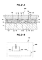
- FIGS. 20A to 23A are cross sectional views showing the connection modes of the capacitance element C in accordance with the modes of arrangement of the conductive layers 15 and the posts 16 in the semiconductor device 200.
- FIGS. 20B to 23B show the corresponding equivalent circuit diagrams.
- FIG. 20A shows the first connection mode of the capacitance element in the second embodiment of the present invention, covering the case where the dielectric material layer 18 is formed in the clearance between the adjacent pieces of the conductive layer 15 so as to form the capacitance element C, and the post 16 is formed in each piece of the conductive layer 15 so as to permit the conductive layer 15 to be connected to the external connection terminals T1 and T2.
- the post 16 is formed on the piece of the conductive layer 15, which is not involved in the formation of the capacitance element, so as to be connected to the external connection terminal T3.
- the both ends of the capacitance element C are connected to only the external connection terminals T1 and T2, respectively, as shown in FIG. 20B.
- FIG. 21A shows the second connection mode of the capacitance element in the second embodiment of the present invention, covering the case where the dielectric material layer 18 is formed in the clearance between the pieces of the conductive layer 15 which are connected to the connection pads 12-1 and 12-2, and the post 16 is not formed on the piece of the conductive layer 15 involved in the formation of the capacitance element C.
- the post 16 is formed on the piece of the conductive layer 15, which is not involved in the formation of the capacitance element, so as to be connected to the external connection terminal T3.
- both the ends of the capacitance element C are connected to only the circuit element of the circuit element-forming region DA, as shown in FIG. 21B.
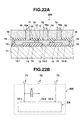
- FIG. 22A shows the third connection mode of the capacitance element in the second embodiment of the present invention, covering the case where the dielectric material layer 18 is arranged in the clearance between those pieces of the adjacent conductive layers 15 which are connected to the connection pads 12-1 and 12-2 so as to form the capacitance element C, and the posts 16 are formed on those pieces of the conductive layers 15 which are involved in the formation of the capacitance element C so as to be connected to the external connection terminals T1 and T2.
- the ports or post 16 is also formed on that the conductive layers or layer 15, which is not involved in the formation of the capacitance element, so as to be connected to the external connection terminal terminals or T3.
- the both ends of the capacitance element C are connected to the circuit element in the circuit element-forming region DA and to the external connection terminals T1 and T2, as shown in FIG. 22B.
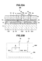
- FIG. 23A shows the fourth connection mode of the capacitance element in the second embodiment of the present invention, covering the case where the dielectric material layer 18 is formed in the clearance between those pieces of the conductive layers 15 which are connected to the connection pad 12-1 and the connection pad 12-2, respectively, so as to form the capacitance element C, and the post 16 is formed on one of these pieces of the conductive layers 15 which are connected to the connection pads 12-1 and 12-2 so as to be connected to the external connection terminal T2.
- the post 16 is also formed on that piece of the conductive layer 15 which is not involved in the formation of the capacitance element C so as to be connected to the external connection terminal T3.
- one end of the capacitance element C is connected to the circuit element in the circuit element-forming region DA, with the other end being connected to both the circuit element in the circuit element-forming region DA and the external connection terminal T2, as shown in FIG. 23B.
- a planar capacitance element is formed in the circuit element-forming region DA in a three dimensional direction so as to be connected to the circuit element.
- the particular construction makes it possible to mount the capacitance element without increasing the chip area. As a result, it is possible to diminish the chip area.
- the capacitance element which was required to be mounted outside the chip in the prior art, can be mounted within the chip in the case of constructing a module equipped with, for example, the wireless I/F function, the particular construction of the present invention contributes to the miniaturization of the module size.
- a ground layer made of the material equal to that of the conductive layer 15 in a position in the vicinity of the plane flush with the conductive layer 15.
- FIG. 24 is a cross sectional view showing the semiconductor device 200 according to a third embodiment of the present invention, with FIGS. 25A and 25B showing the gist portion of the semiconductor device 200 excluding the sealing layer 17 in the cross section along the line III-III shown in FIG. 24.
- the members of the semiconductor device common with those of the semiconductor device according to the first embodiment of the present invention are denoted by the same reference numerals so as to avoid an overlapping description.
- the semiconductor device comprises a plurality of the conductive layers 15 arranged adjacent to each other on the first protective layer 14 and posts 16b arranged adjacent to each other on the conductive layers 15.
- the dielectric material layer 18 is formed in the clearances between the opposite sides of the adjacent conductive layers 15 and between the adjacent posts 16b.
- the dielectric material layer 18 forming the thin film passive element is sandwiched between the adjacent the conductive layers 15 and between the adjacent posts 16b so as to form a planar capacitance element C.
- each of the posts 16b having the dielectric material layer 18 sandwiched therebetween is preferably formed in the shape of a column having a rectangular cross section or in the shape of a plate.
- the particular construction makes it possible to increase the area of the dielectric material layer 18, compared with the second embodiment described previously, so as to increase the capacitance value of the capacitance element C. Incidentally, it is possible for the dielectric material layer 18 to be sandwiched between the plate-like posts 16b alone.
- the planar capacitance element C thus formed can be arranged in various modes on the chip in accordance with the shapes of the conductive layer 15 and the posts 16b having the dielectric material layer 18 sandwiched therebetween.
- the capacitance element C is arranged as shown in FIG. 25A or 25B, it is possible to further increase the area of the dielectric material layer 18 so as to make it possible to form the capacitance element C having a large capacitance.
- the dielectric material layer 18 is sandwiched between the adjacent the conductive layers 15 and between the adjacent posts 16b so as to form a planar capacitance element.
- the particular construction makes it possible to mount a capacitance element larger than that in the second embodiment. It follows that it is possible to further miniaturize the chip area. It is also possible to further miniaturize the module size in the case of constructing a module equipped with, for example, the wireless I/F function.
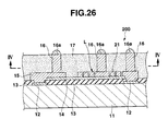
- FIG. 26 is a cross sectional view showing the semiconductor device 200 according to a fourth embodiment of the present invention, with FIGS. 27A and 27B showing the gist portion of the semiconductor device 200 excluding the sealing layer 17 in the cross section along the line IV-IV shown in FIG. 26.
- the members of the semiconductor device common with those of the semiconductor device according to the first embodiment of the present invention are denoted by the same reference numerals so as to avoid an overlapping description.
- the semiconductor device 200 comprises the conductive layers 15 connected to the connection pads 12 and a conductive layer 21 patterned to generate an inductance component, each of these conductive layers 15 and 21 being formed on the first protective layer 14, as shown in FIG. 26.
- an inductance element L acting as a thin film passive element is formed in the semiconductor device 200.
- one end of the inductance element L is connected to the connection pad 12 via the conductive layer 21 so as to be connected to the circuit element in the circuit element-forming region DA, and the post 16 is formed in contact with the conductive layer 21.
- the post 16 is formed on the side of the other end of the inductance element L.
- the conductive layer 21 forming the inductance element is shaped to generate the inductance component.
- the conductive layer 21 is shaped like, for example, an angular eddy form, a rectangular wave form or a loop form.
- the inductance element L of the particular construction which is formed in the circuit element-forming region DA of the semiconductor substrate 11, can be arranged in various modes, as required. For example, it is possible to arrange the inductance element L, which is patterned in an angular eddy form and formed in a relatively large size in a manner to have a relatively large inductance component, as shown in FIG. 27A. It is also possible to arrange a plurality of inductance elements L side by side as shown in FIG. 27B.
- FIGS. 28 to 32 are cross sectional views collectively showing the method of manufacturing the semiconductor device 200 according to the fourth embodiment of the present invention. The manufacturing method will now be described with reference to these drawings.
- a passivation film 13 consisting of, for example, silicon oxide or silicon nitride is formed first on the upper surface of a plurality of connection pads 12 consisting of, for example, aluminum electrodes formed in each chip-forming region in a manner to expose the central portion of each of the connection pads 12, followed by forming the first protective layer 14 on the upper surface of the passivation film 13 in a manner to form an opening in the central portion of each connection pad 12, as shown in FIG. 28.
- the first protective film 14 is formed by coating the entire surface on the circuit side of the semiconductor wafer 100 with a polyimide series resin material and, then, curing the coated resin material, followed by peeling off the resist after a resist patterning and a protective film patterning are applied by using an etching solution.
- a printing method using a squeegee and a coating method utilizing an ink ejection from a nozzle it is also possible to employ a printing method using a squeegee and a coating method utilizing an ink ejection from a nozzle.
- the material of the protective film is not limited to the polyimide series resin material. Specifically, it is also possible to use an epoxy series resin material or PBO (benzaoxidole series) as a material of the protective film.
- the first conductive layers or layer 15 and the conductive layers or layer 21 forming at least one inductance element L are formed on the connection pads 12 exposed through the open portions formed in the first protective film 14, as shown in FIG. 29.
- a UBM layer (not shown) is deposited on the entire surface of the first protective film 14 by, for example, a UBM sputtering method, followed by coating and curing a photoresist for each of the conductive layer 15 and the conductive layer 21 for forming the inductance element.
- a patterning of a predetermined shape is applied by the photolithography technology, followed by applying an electroplating to the portions opened by the resist. It is also possible to employ an electroless plating for forming the conductive layer 15 and the conductive layer 21 for forming the inductance element L.
- the wiring material used for forming the conductive layer includes, for example, copper, aluminum and gold each having good conductive properties.
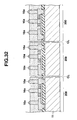
- the posts 16 are formed in predetermined positions on the conductive layer 15 and the conductive layer 21, as shown in FIG. 30.
- a photoresist for the post formation is coated in a thickness of, for example, at least 50 ⁇ m and, typically 100 to 150 ⁇ m, followed by curing the coated photoresist.
- open portions exposing predetermined positions of the conductive layer 15 and the inductance element L are formed in the cured photoresist, followed by applying an electroplating to the open portions noted above so as to form the posts 16. It is also possible to employ the electroless plating method and the stud bump method for forming the post 16.
- the material of the post 16 includes, for example, copper, a solder, gold and nickel each having good conductive characteristics. Where a solder is used as a material for forming the post 16, it is possible to form a spherical electrode by applying a reflow treatment to the solder. Also, in the case of forming the post 16 by using a solder, it is also possible to employ a printing method in addition to the method described above.
- the sealing film 17 is formed by, for example, molding the entire circuit surface of the semiconductor wafer 100 with a resin material such as an epoxy resin in a manner to cover the posts 16, as shown in FIG. 31.
- a resin material such as an epoxy resin
- the sealing film 17 it is possible to employ, for example, a printing method, a dipping method, a spin coating method or a die coating method.
- the upper surface of the sealing film 17 is cut and polished so as to expose the edge surface 16a of the post 16, followed by removing the oxide film from the surface and, then, applying a metallizing treatment such as a solder plating to the edge surface 16a, as shown in FIG. 32. Further, dicing is applied along the cut lines CL conforming with the chip forming regions so as to divide the semiconductor wafer 100 into the individual chip forming regions, thereby forming the individual semiconductor substrates 11. In this fashion, the semiconductor device 200 of the construction as shown in FIG. 26 is obtained.
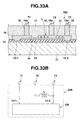
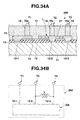
- FIGS. 33A to 36A are cross sectional views showing the connection modes of the inductance element L in accordance with the modes of arrangement of the conductive layer 21 and the posts 16 in the semiconductor device 200.
- FIGS. 33B to 36B show the corresponding equivalent circuit diagrams.
- FIG. 33A shows the first connection mode of the inductance element in the fourth embodiment of the present invention, covering the case where the inductance element L is formed on the conductive layer 21 connected to the connection pad 12-2, and the posts 16 are formed on both edges of the conductor 21 so as to be connected to the external connection terminals T2 and T3.
- the post 16 is also formed on the conductor 15, which is not involved in the formation of the inductance element, so as to be connected to the external connection terminal T1.
- one end of the inductance element L is connected to the circuit element in the circuit element-forming region DA and to the external connection terminal T3.
- the other end of the inductance element L is also connected to the external connection terminal T2.
- FIG. 34A shows the second connection mode of the inductance element according to the fourth embodiment of the present invention, covering the case where the both ends of the conductive layer 21 forming the inductance element L are connected to the connection pad 12-2 and to the connection pad 12-3, respectively, and the posts 16 are mounted to the both edges of the inductance element L formed by the conductive layer 21 so as to be connected to the external connection terminals T2, T3.
- the post 16 is also mounted to the conductive layer 15, which is not involved in the formation of the inductance element L, so as to be connected to the external connection terminal T1.
- both ends of the inductance element L are connected to the circuit element in the circuit element-forming region DA and also connected to the external connection terminals T2 and T3, as shown in FIG. 34B.
- FIG. 35A shows the third connection mode of the inductance element according to the fourth embodiment of the present invention, covering the case where the both ends of the conductive layer 21 forming the inductance element L are connected to the connection pad 12-2 and the connection pad 12-3, and the post 16 is mounted to the conductive layer 15, which is not involved in the formation of the inductance element, so as to be connected to the external connection terminal T1.
- both ends of the inductance element L are connected to only the circuit element in the circuit element-forming region DA.
- FIG. 36A shows the fourth connection mode of the inductance element according to the fourth embodiment of the present invention, covering the case where the posts 16 are mounted to both ends of the conductive layer 21 forming the inductance element L so as to be connected to the external connection terminals T2, T3, and the conductive layer 21 is not connected to the connection pad.
- the post 16 is mounted to the conductive layer 15, which is not involved in the formation of the inductance element, so as to be connected to the external connection terminal T1.
- one end and the other end of the inductance element L are connected to only the external connection terminals T2 and T3, as shown in FIG. 36B.
- the inductance element is stacked on the circuit element-forming region DA so as to be connected to the circuit element, making it possible to mount the inductance element without inviting an increase in the chip area. As a result, it is possible to diminish the chip area.
- the inductance element which was required to be mounted outside the chip in the prior art, can be mounted within the chip so as to contribute to the miniaturization of the module size in the case of constructing a module equipped with, for example, a wireless I/F function.
- the inductance element L is formed of the single conductive layer 21.
- a ground layer made of the material equal to that of the conductive layer 21 in a position in the vicinity of the plane flush with the conductive layer 21.
- FIG. 37 is a cross sectional view showing the semiconductor device 200 according to a fifth embodiment of the present invention.
- the members of the semiconductor device common with those of the semiconductor device according to the fourth embodiment of the present invention are denoted by the same reference numerals so as to avoid an overlapping description.
- a third protective film 22 is formed on the conductive layer 21 forming the inductance element L as a thin film passive element and on the conductive layer 15, as shown in FIG. 37.
- the inductance element L is sandwiched between the first protective film 14 and the third protective film 22 so as to make it possible to obtain stable inductance characteristics.
- the conductive layer 15 and the conductive layer 21 forming the inductance element L are formed first. Then, the entire surface on the circuit side of the semiconductor wafer is coated with a polyimide series resin material, followed by curing the coated resin material like the first protective film 14 described previously. Further, a resist patterning and a protective film patterning are applied by using an etching solution, followed by peeling off the resist, thereby forming the third protective film 22.
- FIG. 38 is a cross sectional view showing the semiconductor device 200 according to a sixth embodiment of the present invention.
- the members of the semiconductor device common with those of the semiconductor device according to the fourth embodiment of the present invention are denoted by the same reference numerals so as to avoid an overlapping description.
- a magnetic film 23 is formed on the inductance element L forming a thin film passive element with the third protective film 22 interposed therebetween, in addition to the construction of the semiconductor device according to the fifth embodiment of the present invention.
- the magnetic film 23 can be formed of a ferromagnetic material.
- the magnetic film 23 can be formed by mixing a ferromagnetic material or a soft magnetic material in, for example, a resin.
- the magnetic film 23 on the inductance element L with the third protective film 22 interposed therebetween it is possible to markedly increase the inductance value of the inductance element L so as to improve the characteristics as the inductance element. As a result, it is possible to diminish the size of the conductive layer 21 required for obtaining the same inductance value. It is also possible to improve the inductance characteristics.
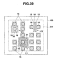
- each embodiment of the present invention it is possible to integrally stack the capacitance element or the inductance element forming a passive element on the circuit element-forming region DA of the semiconductor device 200. Needless to say, it is possible for the capacitance element and the inductance element according to each embodiment of the present invention to be present in a mixed fashion on the circuit element-forming region DA. For example, as shown in FIG.
Landscapes
- Semiconductor Integrated Circuits (AREA)
Abstract
Description
In these drawings, the members of the semiconductor device common with those of the semiconductor device according to the first embodiment of the present invention are denoted by the same reference numerals so as to avoid an overlapping description.
The wiring material used for forming the conductive layer includes, for example, copper, aluminum and gold each having good conductive properties.
As a result, it is possible to diminish the chip area. In addition, the inductance element, which was required to be mounted outside the chip in the prior art, can be mounted within the chip so as to contribute to the miniaturization of the module size in the case of constructing a module equipped with, for example, a wireless I/F function.
Claims (25)
- A semiconductor device, comprising:a semiconductor substrate (11) including a circuit element-forming region (DA) and a plurality of connection pads (12);an insulating film (14) formed on said circuit element-forming region (DA); anda columnar electrode (16) electrically connected to at least one of said plural connection pads (12), characterized by further comprisingat least one thin film passive element including at least one conductive layer formed on said insulating film (14).
- The semiconductor device according to claim 1, characterized in that said thin film passive element is at least one capacitance element (C).
- The semiconductor device according to claim 2, characterized in that said capacitance element (C) includes two conductive layers (15, 20) and a dielectric material layer (18), said two conductive layers (15, 20) stacked one upon the other on said insulating film, and said dielectric material layer (18) is interposed between the conductive layers (15, 20).
- The semiconductor device according to claim 2, characterized in that said capacitance element (C) includes two conductive layers (15, 20) and a dielectric material layer (18), said two conductive layer (15) positioned apart from each other on said insulating film, and said dielectric layer (18) is formed in the clearance between the two adjacent conductive layers (15).
- The semiconductor device according to claim 2, characterized in that said capacitance element (C) includes two conductive layers (15,20) and a dielectric material layer (18), said two conductive layers (15) positioned adjacent to and apart from each other on said insulating film and a plate-like electrode (16b) positioned on the conductor layers (15), and said dielectric material layer (18) is formed in the clearance between the opposite ends of the adjacent plate-like electrodes (16b).
- The semiconductor device according to claim 1, characterized in that said thin film passive element is at least one inductance element (L).
- The semiconductor device according to claim 6, characterized in that said inductance element (L) includes one conductive layer, said conductive layer (21) being formed in the shape of any of an angular eddy shape, a rectangular wave shape, and a loop shape.
- The semiconductor device according to claim 7, characterized in that said inductance element (L) further comprises a magnetic film (23) on said conductive layer (21).
- The semiconductor device according to claim 1, characterized in that said thin film passive element includes two terminal electrodes, at least one of said two terminal electrodes of said thin film passive element being electrically connected to said columnar electrode (16).
- The semiconductor device according to claim 1, characterized in that said thin film passive element includes two terminal electrodes, at least one of said two terminal electrodes of said thin film passive element being electrically connected to said connection pad (12).
- The semiconductor device according to claim 1, characterized in that said thin film passive element includes two terminal electrodes, each of said terminal electrodes of said thin film passive element being connected to at least one of said connection pad (12) and said columnar electrode (16).
- The semiconductor device according to claim 1, characterized in that the periphery of said thin film passive element is covered with a protective film (19, 22).
- The semiconductor device according to claim 1, characterized by further comprising a plurality of said thin film passive elements.
- A method of manufacturing a semiconductor device characterized by comprising the steps of:preparing a semiconductor wafer substrate (100) including a plurality of chip forming regions each having a circuit element-forming region (DA) and a plurality of connection pads (12);forming an insulating film (14) on the circuit element-forming region (DA) of each of said chip forming regions;forming at least one thin film passive element including at least one conductive layer on said insulating film (14);forming a columnar electrode (16) electrically connected to at least one of said plural connection pads (12); anddividing said semiconductor wafer substrate (100) into individual chip forming regions so as to form a plurality of semiconductor devices (200) each having at least one thin film passive element.
- The method of manufacturing a semiconductor device according to claim 14, characterized in that said step of forming said thin film passive element comprises sub-steps of forming at least one of a capacitance element (C).
- The method of manufacturing a semiconductor device according to claim 15, characterized in that said step of forming a capacitance element (C) comprises the sub-steps of:forming a first conductive layer (15) on the circuit element-forming region of said semiconductor substrate with an insulating film (14) interposed therebetween;forming a dielectric material layer (18) on said first conductive layer (15); andforming a second conductive layer (20) on said dielectric material layer (18).
- The method of manufacturing a semiconductor device according to claim 15, characterized in that said step of forming the capacitance element (C) comprises the sub-steps of:forming two pieces of conductive layer (15) positioned adjacent to each other a predetermined distance apart from each other on said insulating film (14); andforming a dielectric material layer (18) in the clearance between adjacent two pieces of said conductive layer (15).
- The method of manufacturing a semiconductor device according to claim 15, characterized in that said step of forming the capacitance element (C) comprises the sub-steps of:forming two pieces of the conductive layer (15) positioned adjacent to each other a predetermined distance apart from each other on said insulating film (14);forming a plate-like electrode (16b) on each of the two adjacent pieces of said conductive layer (15); andforming a dielectric material layer (18) in the clearance between one end and the other end of said plate-like electrodes (16b).
- The method of manufacturing a semiconductor device according to claim 14, characterized in that said forming of said thin film passive element comprises forming at least one inductance element (L).
- The method of manufacturing a semiconductor device according to claim 19, characterized in that said step of forming the inductance element (L) comprises the sub-step of patterning said conductive layer (21) in any of the shapes selected from the group consisting of an angular eddy shape, a rectangular wave shape and a loop shape.
- The method of manufacturing a semiconductor device according to claim 20, characterized in that said step of forming the inductance element (L) as said thin film passive element comprises the sub-step of forming a magnetic film (23) on said second conductive layer (21).
- The method of manufacturing a semiconductor device according to claim 14, characterized in that said step of forming said thin film passive element comprises the sub-step of covering the periphery of said thin film passive element with a protective film (19,22).
- The method of manufacturing a semiconductor device according to claim 14, characterized in that said step of forming said thin film passive element comprises the sub-step of forming said columnar electrode (16) in at least one of the electrode terminals at one end and the other end of said thin film passive element.
- The method of manufacturing a semiconductor device according to claim 14, characterized in that said step of forming said thin film passive element comprises the sub-step of connecting at least one of the electrode terminals at one end and the other end of said thin film passive element to said connection pad (12).
- The method of manufacturing a semiconductor device according to claim 14, characterized in that said step of forming said thin film passive element comprises the sub-step of connecting each electrode terminal of said thin film passive element to at least one of said connection pad (12) and said columnar electrode (16).
Applications Claiming Priority (4)
| Application Number | Priority Date | Filing Date | Title |
|---|---|---|---|
| JP2000243765A JP3540728B2 (en) | 2000-08-11 | 2000-08-11 | Semiconductor device and method of manufacturing semiconductor device |
| JP2000243783A JP3540729B2 (en) | 2000-08-11 | 2000-08-11 | Semiconductor device and manufacturing method of semiconductor device |
| JP2000243765 | 2000-08-11 | ||
| JP2000243783 | 2000-08-11 |
Publications (3)
| Publication Number | Publication Date |
|---|---|
| EP1182703A2 true EP1182703A2 (en) | 2002-02-27 |
| EP1182703A3 EP1182703A3 (en) | 2005-09-28 |
| EP1182703B1 EP1182703B1 (en) | 2019-01-23 |
Family
ID=26597796
Family Applications (1)
| Application Number | Title | Priority Date | Filing Date |
|---|---|---|---|
| EP01119376.0A Expired - Lifetime EP1182703B1 (en) | 2000-08-11 | 2001-08-10 | Semiconductor device having integrated capacitor and/or inductor |
Country Status (6)
| Country | Link |
|---|---|
| US (1) | US6847066B2 (en) |
| EP (1) | EP1182703B1 (en) |
| KR (1) | KR100443954B1 (en) |
| CN (1) | CN1177368C (en) |
| SG (1) | SG99939A1 (en) |
| TW (1) | TW515015B (en) |
Cited By (11)
| Publication number | Priority date | Publication date | Assignee | Title |
|---|---|---|---|---|
| WO2003065448A1 (en) * | 2002-01-29 | 2003-08-07 | Siemens Aktiengesellschaft | Chip-size package with an integrated passive component |
| WO2003085731A1 (en) * | 2002-04-11 | 2003-10-16 | Koninklijke Philips Electronics N.V. | Semiconductor device and method of manufacturing same |
| WO2003085729A1 (en) * | 2002-04-11 | 2003-10-16 | Koninklijke Philips Electronics N.V. | Method of manufacturing an electronic device |
| WO2003094233A1 (en) * | 2002-04-29 | 2003-11-13 | Infineon Technologies Ag | Integrated circuit with integrated capacitor and methods for making same |
| WO2004047169A1 (en) * | 2002-11-21 | 2004-06-03 | Casio Computer Co., Ltd. | High frequency signal transmission structure |
| EP1359618A3 (en) * | 2001-04-17 | 2005-02-09 | Casio Computer Co., Ltd. | Semiconductor device |
| DE10335153A1 (en) * | 2003-07-31 | 2005-03-03 | Siemens Ag | Circuit arrangement on a substrate and method for producing the circuit arrangement on the substrate |
| FR2867609A1 (en) * | 2004-03-12 | 2005-09-16 | United Monolithic Semiconduct | MINIATURE MICROWAVE POWER UNIT AND METHOD FOR MANUFACTURING THE HOUSING |
| DE102005008195A1 (en) * | 2005-02-23 | 2006-08-24 | Atmel Germany Gmbh | RF arrangement |
| CN100338817C (en) * | 2003-08-28 | 2007-09-19 | 索尼株式会社 | Substrate having microstrip line structure, semiconductor device having microstrip line structure, and manufacturing method of substrate having microstrip line structure |
| EP3193366A3 (en) * | 2008-07-25 | 2017-08-16 | ATI Technologies ULC | Under bump metallization for on-die capacitor |
Families Citing this family (84)
| Publication number | Priority date | Publication date | Assignee | Title |
|---|---|---|---|---|
| US6495442B1 (en) | 2000-10-18 | 2002-12-17 | Magic Corporation | Post passivation interconnection schemes on top of the IC chips |
| US8421158B2 (en) * | 1998-12-21 | 2013-04-16 | Megica Corporation | Chip structure with a passive device and method for forming the same |
| US6965165B2 (en) | 1998-12-21 | 2005-11-15 | Mou-Shiung Lin | Top layers of metal for high performance IC's |
| US6869870B2 (en) * | 1998-12-21 | 2005-03-22 | Megic Corporation | High performance system-on-chip discrete components using post passivation process |
| US7381642B2 (en) * | 2004-09-23 | 2008-06-03 | Megica Corporation | Top layers of metal for integrated circuits |
| US7405149B1 (en) * | 1998-12-21 | 2008-07-29 | Megica Corporation | Post passivation method for semiconductor chip or wafer |
| US6303423B1 (en) * | 1998-12-21 | 2001-10-16 | Megic Corporation | Method for forming high performance system-on-chip using post passivation process |
| US8178435B2 (en) | 1998-12-21 | 2012-05-15 | Megica Corporation | High performance system-on-chip inductor using post passivation process |
| US7531417B2 (en) * | 1998-12-21 | 2009-05-12 | Megica Corporation | High performance system-on-chip passive device using post passivation process |
| JP3465617B2 (en) | 1999-02-15 | 2003-11-10 | カシオ計算機株式会社 | Semiconductor device |
| US7372161B2 (en) * | 2000-10-18 | 2008-05-13 | Megica Corporation | Post passivation interconnection schemes on top of the IC chips |
| US7271489B2 (en) | 2003-10-15 | 2007-09-18 | Megica Corporation | Post passivation interconnection schemes on top of the IC chips |
| US7498196B2 (en) * | 2001-03-30 | 2009-03-03 | Megica Corporation | Structure and manufacturing method of chip scale package |
| US6744114B2 (en) * | 2001-08-29 | 2004-06-01 | Honeywell International Inc. | Package with integrated inductor and/or capacitor |
| US6759275B1 (en) * | 2001-09-04 | 2004-07-06 | Megic Corporation | Method for making high-performance RF integrated circuits |
| US6673698B1 (en) | 2002-01-19 | 2004-01-06 | Megic Corporation | Thin film semiconductor package utilizing a glass substrate with composite polymer/metal interconnect layers |
| TW584950B (en) | 2001-12-31 | 2004-04-21 | Megic Corp | Chip packaging structure and process thereof |
| TW517361B (en) * | 2001-12-31 | 2003-01-11 | Megic Corp | Chip package structure and its manufacture process |
| TW503496B (en) * | 2001-12-31 | 2002-09-21 | Megic Corp | Chip packaging structure and manufacturing process of the same |
| TW544882B (en) * | 2001-12-31 | 2003-08-01 | Megic Corp | Chip package structure and process thereof |
| TW577160B (en) * | 2002-02-04 | 2004-02-21 | Casio Computer Co Ltd | Semiconductor device and manufacturing method thereof |
| JP3829325B2 (en) * | 2002-02-07 | 2006-10-04 | 日本電気株式会社 | Semiconductor element, manufacturing method thereof, and manufacturing method of semiconductor device |
| JP3616605B2 (en) * | 2002-04-03 | 2005-02-02 | 沖電気工業株式会社 | Semiconductor device |
| JP3871609B2 (en) * | 2002-05-27 | 2007-01-24 | 松下電器産業株式会社 | Semiconductor device and manufacturing method thereof |
| CN1568546B (en) | 2002-08-09 | 2010-06-23 | 卡西欧计算机株式会社 | Semiconductor device and manufacturing method thereof |
| JP3808030B2 (en) * | 2002-11-28 | 2006-08-09 | 沖電気工業株式会社 | Semiconductor device and manufacturing method thereof |
| US7319277B2 (en) * | 2003-05-08 | 2008-01-15 | Megica Corporation | Chip structure with redistribution traces |
| DE10323007B4 (en) * | 2003-05-21 | 2005-10-20 | Infineon Technologies Ag | A semiconductor device |
| TWI236763B (en) * | 2003-05-27 | 2005-07-21 | Megic Corp | High performance system-on-chip inductor using post passivation process |
| JP2005005409A (en) * | 2003-06-11 | 2005-01-06 | Matsushita Electric Ind Co Ltd | Semiconductor device |
| TWI228814B (en) * | 2003-06-26 | 2005-03-01 | United Microelectronics Corp | Parasitic capacitance-preventing dummy solder bump structure and method of making the same |
| JP4360873B2 (en) * | 2003-09-18 | 2009-11-11 | ミナミ株式会社 | Manufacturing method of wafer level CSP |
| GB2406720B (en) * | 2003-09-30 | 2006-09-13 | Agere Systems Inc | An inductor formed in an integrated circuit |
| US7462942B2 (en) * | 2003-10-09 | 2008-12-09 | Advanpack Solutions Pte Ltd | Die pillar structures and a method of their formation |
| US7459790B2 (en) | 2003-10-15 | 2008-12-02 | Megica Corporation | Post passivation interconnection schemes on top of the IC chips |
| US7394161B2 (en) * | 2003-12-08 | 2008-07-01 | Megica Corporation | Chip structure with pads having bumps or wirebonded wires formed thereover or used to be tested thereto |
| JP3851320B2 (en) * | 2004-03-25 | 2006-11-29 | Tdk株式会社 | Circuit device and manufacturing method thereof |
| JP4746847B2 (en) * | 2004-04-27 | 2011-08-10 | 三洋電機株式会社 | Manufacturing method of semiconductor device |
| JP2006041401A (en) * | 2004-07-29 | 2006-02-09 | Sharp Corp | Semiconductor device and manufacturing method thereof |
| JP2006041357A (en) * | 2004-07-29 | 2006-02-09 | Fujikura Ltd | Semiconductor device and manufacturing method thereof |
| SG119329A1 (en) * | 2004-07-29 | 2006-02-28 | Fujikura Ltd | Semiconductor device and method for manufacturing the same |
| US7355282B2 (en) * | 2004-09-09 | 2008-04-08 | Megica Corporation | Post passivation interconnection process and structures |
| US7423346B2 (en) * | 2004-09-09 | 2008-09-09 | Megica Corporation | Post passivation interconnection process and structures |
| US8008775B2 (en) * | 2004-09-09 | 2011-08-30 | Megica Corporation | Post passivation interconnection structures |
| JP4972306B2 (en) * | 2004-12-21 | 2012-07-11 | オンセミコンダクター・トレーディング・リミテッド | Semiconductor device and circuit device |
| US8384189B2 (en) | 2005-03-29 | 2013-02-26 | Megica Corporation | High performance system-on-chip using post passivation process |
| US7468545B2 (en) * | 2005-05-06 | 2008-12-23 | Megica Corporation | Post passivation structure for a semiconductor device and packaging process for same |
| TWI330863B (en) | 2005-05-18 | 2010-09-21 | Megica Corp | Semiconductor chip with coil element over passivation layer |
| JP4265575B2 (en) * | 2005-06-21 | 2009-05-20 | セイコーエプソン株式会社 | Semiconductor chip and electronic equipment |
| US7582556B2 (en) | 2005-06-24 | 2009-09-01 | Megica Corporation | Circuitry component and method for forming the same |
| JP4235834B2 (en) * | 2005-07-12 | 2009-03-11 | セイコーエプソン株式会社 | Manufacturing method of semiconductor device |
| CN1901162B (en) * | 2005-07-22 | 2011-04-20 | 米辑电子股份有限公司 | Method for manufacturing circuit assembly by continuous electroplating and circuit assembly structure |
| JP4289335B2 (en) * | 2005-08-10 | 2009-07-01 | セイコーエプソン株式会社 | Electronic components, circuit boards and electronic equipment |
| US7473999B2 (en) * | 2005-09-23 | 2009-01-06 | Megica Corporation | Semiconductor chip and process for forming the same |
| JP2008159820A (en) * | 2006-12-22 | 2008-07-10 | Tdk Corp | Electronic component batch mounting method and electronic component built-in substrate manufacturing method |
| JP4980709B2 (en) * | 2006-12-25 | 2012-07-18 | ローム株式会社 | Semiconductor device |
| US8749021B2 (en) * | 2006-12-26 | 2014-06-10 | Megit Acquisition Corp. | Voltage regulator integrated with semiconductor chip |
| FR2911006A1 (en) * | 2007-01-03 | 2008-07-04 | St Microelectronics Sa | Integrated electronic circuit chip for electronic circuit assembly e.g. filter, has inductor arranged above protective layer, where thickness of inductor is extended from and beyond upper surface of protective layer |
| US8749065B2 (en) * | 2007-01-25 | 2014-06-10 | Tera Probe, Inc. | Semiconductor device comprising electromigration prevention film and manufacturing method thereof |
| TWI397158B (en) * | 2007-02-13 | 2013-05-21 | 兆裝微股份有限公司 | Semiconductor device mixed with magnetic powder and method of manufacturing same |
| US7820520B2 (en) * | 2007-03-22 | 2010-10-26 | Freescale Semiconductor, Inc. | Semiconductor device with capacitor and/or inductor and method of making |
| US7777339B2 (en) * | 2007-07-30 | 2010-08-17 | International Business Machines Corporation | Semiconductor chips with reduced stress from underfill at edge of chip |
| JP5268345B2 (en) * | 2007-12-20 | 2013-08-21 | パナソニック株式会社 | Inductor |
| US8035224B2 (en) * | 2008-11-14 | 2011-10-11 | Infineon Technologies Ag | Semiconductor device |
| US20100165585A1 (en) * | 2008-12-26 | 2010-07-01 | Megica Corporation | Chip packages with power management integrated circuits and related techniques |
| US9543262B1 (en) * | 2009-08-18 | 2017-01-10 | Cypress Semiconductor Corporation | Self aligned bump passivation |
| TWI528514B (en) * | 2009-08-20 | 2016-04-01 | 精材科技股份有限公司 | Chip package and method of manufacturing same |
| CN103814439B (en) * | 2011-09-09 | 2016-10-19 | 株式会社村田制作所 | Module substrate |
| US20130146345A1 (en) * | 2011-12-12 | 2013-06-13 | Kazuki KAJIHARA | Printed wiring board and method for manufacturing the same |
| US9960106B2 (en) * | 2012-05-18 | 2018-05-01 | Taiwan Semiconductor Manufacturing Co., Ltd. | Package with metal-insulator-metal capacitor and method of manufacturing the same |
| US9087779B2 (en) * | 2013-01-02 | 2015-07-21 | Maxim Integrated Products, Inc. | Multi-die, high current wafer level package |
| KR101983137B1 (en) * | 2013-03-04 | 2019-05-28 | 삼성전기주식회사 | Power inductor and manufacturing method thereof |
| US9000587B1 (en) * | 2013-03-12 | 2015-04-07 | Maxim Integrated Products, Inc. | Wafer-level thin chip integration |
| US9231046B2 (en) * | 2013-03-15 | 2016-01-05 | Globalfoundries Inc. | Capacitor using barrier layer metallurgy |
| US10833144B2 (en) * | 2016-11-14 | 2020-11-10 | Advanced Semiconductor Engineering, Inc. | Semiconductor device packages including an inductor and a capacitor |
| WO2018123926A1 (en) | 2016-12-28 | 2018-07-05 | 株式会社村田製作所 | Thin film device and method for manufacturing thin film device |
| US10244632B2 (en) * | 2017-03-02 | 2019-03-26 | Intel Corporation | Solder resist layer structures for terminating de-featured components and methods of making the same |
| US10304804B2 (en) * | 2017-03-31 | 2019-05-28 | Intel Corporation | System on package architecture including structures on die back side |
| TWI672840B (en) * | 2017-07-25 | 2019-09-21 | Siliconware Precision Industries Co., Ltd. | Electronic package and substrate structure and the manufacture thereof |
| WO2019208221A1 (en) * | 2018-04-27 | 2019-10-31 | 株式会社村田製作所 | Capacitor assembly |
| JP2021048204A (en) * | 2019-09-17 | 2021-03-25 | キオクシア株式会社 | Semiconductor devices and their manufacturing methods |
| KR102889512B1 (en) | 2021-01-04 | 2025-11-21 | 삼성전자주식회사 | Semiconductor pacakge |
| CN118299277A (en) * | 2023-01-05 | 2024-07-05 | 星科金朋私人有限公司 | Semiconductor device and method for manufacturing the same |
| US20240355728A1 (en) * | 2023-04-21 | 2024-10-24 | Taiwan Semiconductor Manufacturing Company, Ltd. | Semiconductor structure |
Family Cites Families (33)
| Publication number | Priority date | Publication date | Assignee | Title |
|---|---|---|---|---|
| US4322778A (en) * | 1980-01-25 | 1982-03-30 | International Business Machines Corp. | High performance semiconductor package assembly |
| US4617193A (en) | 1983-06-16 | 1986-10-14 | Digital Equipment Corporation | Planar interconnect for integrated circuits |
| US4811082A (en) * | 1986-11-12 | 1989-03-07 | International Business Machines Corporation | High performance integrated circuit packaging structure |
| DE3641299A1 (en) | 1986-12-03 | 1988-06-16 | Philips Patentverwaltung | INTEGRATED SEMICONDUCTOR CIRCUIT WITH MULTIPLE LAYER WIRING |
| JPH0621348A (en) * | 1991-06-22 | 1994-01-28 | Nec Corp | Semiconductor element |
| CA2072277A1 (en) * | 1991-07-03 | 1993-01-04 | Nobuo Shiga | Inductance element |
| US5317433A (en) * | 1991-12-02 | 1994-05-31 | Canon Kabushiki Kaisha | Image display device with a transistor on one side of insulating layer and liquid crystal on the other side |
| JP3285919B2 (en) | 1992-02-05 | 2002-05-27 | 株式会社東芝 | Semiconductor device |
| JPH05326315A (en) * | 1992-05-25 | 1993-12-10 | Itochu Fine Chem Kk | Thin film capacitor and manufacturing device thereof |
| WO1994017558A1 (en) * | 1993-01-29 | 1994-08-04 | The Regents Of The University Of California | Monolithic passive component |
| US5510758A (en) | 1993-04-07 | 1996-04-23 | Matsushita Electric Industrial Co., Ltd. | Multilayer microstrip wiring board with a semiconductor device mounted thereon via bumps |
| US5530288A (en) * | 1994-10-12 | 1996-06-25 | International Business Machines Corporation | Passive interposer including at least one passive electronic component |
| US5633785A (en) * | 1994-12-30 | 1997-05-27 | University Of Southern California | Integrated circuit component package with integral passive component |
| US6124606A (en) * | 1995-06-06 | 2000-09-26 | Ois Optical Imaging Systems, Inc. | Method of making a large area imager with improved signal-to-noise ratio |
| JP3076507B2 (en) | 1995-06-13 | 2000-08-14 | 松下電子工業株式会社 | Semiconductor device, semiconductor integrated circuit device, and method of manufacturing the same |
| JP2904086B2 (en) * | 1995-12-27 | 1999-06-14 | 日本電気株式会社 | Semiconductor device and manufacturing method thereof |
| JP2830845B2 (en) * | 1996-06-26 | 1998-12-02 | 日本電気株式会社 | Semiconductor storage device |
| US5990507A (en) | 1996-07-09 | 1999-11-23 | Kabushiki Kaisha Toshiba | Semiconductor device having ferroelectric capacitor structures |
| GB9617885D0 (en) | 1996-08-28 | 1996-10-09 | Philips Electronics Nv | Electronic device manufacture |
| US6331722B1 (en) * | 1997-01-18 | 2001-12-18 | Semiconductor Energy Laboratory Co., Ltd. | Hybrid circuit and electronic device using same |
| US5982018A (en) * | 1997-05-23 | 1999-11-09 | Micron Technology, Inc. | Thin film capacitor coupons for memory modules and multi-chip modules |
| JPH1197525A (en) | 1997-09-19 | 1999-04-09 | Hitachi Ltd | Semiconductor device and manufacturing method thereof |
| US5928968A (en) | 1997-12-22 | 1999-07-27 | Vlsi Technology, Inc. | Semiconductor pressure transducer structures and methods for making the same |
| KR100563122B1 (en) | 1998-01-30 | 2006-03-21 | 다이요 유덴 가부시키가이샤 | Hybrid module, manufacturing method thereof and installation method |
| US6108212A (en) * | 1998-06-05 | 2000-08-22 | Motorola, Inc. | Surface-mount device package having an integral passive component |
| JP3419695B2 (en) * | 1998-10-14 | 2003-06-23 | 株式会社日立製作所 | Semiconductor element |
| US6140155A (en) | 1998-12-24 | 2000-10-31 | Casio Computer Co., Ltd. | Method of manufacturing semiconductor device using dry photoresist film |
| KR100431307B1 (en) * | 1998-12-29 | 2004-09-18 | 주식회사 하이닉스반도체 | Capacitor embedded chip size package and manufacturing method thereof |
| US6274937B1 (en) * | 1999-02-01 | 2001-08-14 | Micron Technology, Inc. | Silicon multi-chip module packaging with integrated passive components and method of making |
| US6180976B1 (en) * | 1999-02-02 | 2001-01-30 | Conexant Systems, Inc. | Thin-film capacitors and methods for forming the same |
| JP3465617B2 (en) * | 1999-02-15 | 2003-11-10 | カシオ計算機株式会社 | Semiconductor device |
| US6031293A (en) | 1999-04-26 | 2000-02-29 | United Microelectronics Corporation | Package-free bonding pad structure |
| JP2001060664A (en) * | 1999-08-23 | 2001-03-06 | Mitsubishi Electric Corp | Semiconductor device |
-
2001
- 2001-08-08 US US09/924,293 patent/US6847066B2/en not_active Expired - Lifetime
- 2001-08-08 SG SG200104761A patent/SG99939A1/en unknown
- 2001-08-09 KR KR10-2001-0047844A patent/KR100443954B1/en not_active Expired - Lifetime
- 2001-08-09 TW TW090119509A patent/TW515015B/en not_active IP Right Cessation
- 2001-08-10 EP EP01119376.0A patent/EP1182703B1/en not_active Expired - Lifetime
- 2001-08-13 CN CNB011255811A patent/CN1177368C/en not_active Expired - Lifetime
Cited By (15)
| Publication number | Priority date | Publication date | Assignee | Title |
|---|---|---|---|---|
| EP1359618A3 (en) * | 2001-04-17 | 2005-02-09 | Casio Computer Co., Ltd. | Semiconductor device |
| WO2003065448A1 (en) * | 2002-01-29 | 2003-08-07 | Siemens Aktiengesellschaft | Chip-size package with an integrated passive component |
| WO2003085731A1 (en) * | 2002-04-11 | 2003-10-16 | Koninklijke Philips Electronics N.V. | Semiconductor device and method of manufacturing same |
| WO2003085729A1 (en) * | 2002-04-11 | 2003-10-16 | Koninklijke Philips Electronics N.V. | Method of manufacturing an electronic device |
| WO2003094233A1 (en) * | 2002-04-29 | 2003-11-13 | Infineon Technologies Ag | Integrated circuit with integrated capacitor and methods for making same |
| US7759768B2 (en) | 2002-04-29 | 2010-07-20 | Infineon Technologies Ag | Integrated circuit with intergrated capacitor and methods for making same |
| US7012490B2 (en) | 2002-11-21 | 2006-03-14 | Casio Computer Co., Ltd. | High frequency signal transmission structure |
| WO2004047169A1 (en) * | 2002-11-21 | 2004-06-03 | Casio Computer Co., Ltd. | High frequency signal transmission structure |
| DE10335153A1 (en) * | 2003-07-31 | 2005-03-03 | Siemens Ag | Circuit arrangement on a substrate and method for producing the circuit arrangement on the substrate |
| DE10335153B4 (en) * | 2003-07-31 | 2006-07-27 | Siemens Ag | Circuit arrangement on a substrate having a component of a sensor, and method for producing the circuit arrangement on the substrate |
| CN100338817C (en) * | 2003-08-28 | 2007-09-19 | 索尼株式会社 | Substrate having microstrip line structure, semiconductor device having microstrip line structure, and manufacturing method of substrate having microstrip line structure |
| FR2867609A1 (en) * | 2004-03-12 | 2005-09-16 | United Monolithic Semiconduct | MINIATURE MICROWAVE POWER UNIT AND METHOD FOR MANUFACTURING THE HOUSING |
| DE102005008195A1 (en) * | 2005-02-23 | 2006-08-24 | Atmel Germany Gmbh | RF arrangement |
| US7605450B2 (en) | 2005-02-23 | 2009-10-20 | Atmel Automotive Gmbh | High frequency arrangement |
| EP3193366A3 (en) * | 2008-07-25 | 2017-08-16 | ATI Technologies ULC | Under bump metallization for on-die capacitor |
Also Published As
| Publication number | Publication date |
|---|---|
| KR100443954B1 (en) | 2004-08-11 |
| KR20020014697A (en) | 2002-02-25 |
| HK1045023A1 (en) | 2002-11-08 |
| EP1182703A3 (en) | 2005-09-28 |
| CN1338779A (en) | 2002-03-06 |
| US6847066B2 (en) | 2005-01-25 |
| EP1182703B1 (en) | 2019-01-23 |
| US20020017730A1 (en) | 2002-02-14 |
| CN1177368C (en) | 2004-11-24 |
| SG99939A1 (en) | 2003-11-27 |
| TW515015B (en) | 2002-12-21 |
Similar Documents
| Publication | Publication Date | Title |
|---|---|---|
| EP1182703B1 (en) | Semiconductor device having integrated capacitor and/or inductor | |
| JP3939504B2 (en) | Semiconductor device, method for manufacturing the same, and mounting structure | |
| KR100364058B1 (en) | Semiconductor device and its manufacturing process | |
| US6940385B2 (en) | High-frequency coil device and method of manufacturing the same | |
| US7541278B2 (en) | Interconnect substrate, semiconductor device, methods of manufacturing the same, circuit board, and electronic equipment | |
| US8035192B2 (en) | Semiconductor device and manufacturing method thereof | |
| US7482202B2 (en) | Semiconductor device including a plurality of circuit element chips and a manufacturing method thereof | |
| KR20090066211A (en) | Method of forming semiconductor device and integrated passive device module | |
| JP3540729B2 (en) | Semiconductor device and manufacturing method of semiconductor device | |
| US20070029667A1 (en) | Semiconductor device | |
| JP3540728B2 (en) | Semiconductor device and method of manufacturing semiconductor device | |
| JP4367070B2 (en) | Semiconductor device and manufacturing method thereof | |
| US6356429B2 (en) | Capacitor | |
| US20070176287A1 (en) | Thin integrated circuit device packages for improved radio frequency performance | |
| EP1128435A2 (en) | Microwave electric elements using porous silicon dioxide layer and forming method of same | |
| KR100348250B1 (en) | fabrication method for micro passive element | |
| KR100379900B1 (en) | microwave electric elements fabricated using porous oxidized silicon layer and fabricating method of the same | |
| CN122028754A (en) | Packaging carrier plate, preparation method thereof and semiconductor packaging structure | |
| HK1061468A (en) | Semiconductor device |
Legal Events
| Date | Code | Title | Description |
|---|---|---|---|
| PUAI | Public reference made under article 153(3) epc to a published international application that has entered the european phase |
Free format text: ORIGINAL CODE: 0009012 |
|
| 17P | Request for examination filed |
Effective date: 20010810 |
|
| AK | Designated contracting states |
Kind code of ref document: A2 Designated state(s): AT BE CH CY DE DK ES FI FR GB GR IE IT LI LU MC NL PT SE TR |
|
| AX | Request for extension of the european patent |
Free format text: AL;LT;LV;MK;RO;SI |
|
| RAP1 | Party data changed (applicant data changed or rights of an application transferred) |
Owner name: OKI ELECTRIC INDUSTRY COMPANY, LIMITED Owner name: CASIO COMPUTER CO., LTD. |
|
| PUAL | Search report despatched |
Free format text: ORIGINAL CODE: 0009013 |
|
| AK | Designated contracting states |
Kind code of ref document: A3 Designated state(s): AT BE CH CY DE DK ES FI FR GB GR IE IT LI LU MC NL PT SE TR |
|
| AX | Request for extension of the european patent |
Extension state: AL LT LV MK RO SI |
|
| RIC1 | Information provided on ipc code assigned before grant |
Ipc: 7H 01L 23/31 A Ipc: 7H 01L 23/522 B |
|
| AKX | Designation fees paid |
Designated state(s): DE FR GB NL |
|
| 17Q | First examination report despatched |
Effective date: 20060720 |
|
| RAP1 | Party data changed (applicant data changed or rights of an application transferred) |
Owner name: OKI ELECTRIC INDUSTRY COMPANY, LIMITED Owner name: TERAMIKROS, INC. |
|
| RAP1 | Party data changed (applicant data changed or rights of an application transferred) |
Owner name: LAPIS SEMICONDUCTOR CO., LTD. Owner name: TERAMIKROS, INC. |
|
| RAP1 | Party data changed (applicant data changed or rights of an application transferred) |
Owner name: LAPIS SEMICONDUCTOR CO., LTD. Owner name: TERAMIKROS, INC. |
|
| RAP1 | Party data changed (applicant data changed or rights of an application transferred) |
Owner name: TERA PROBE, INC. Owner name: LAPIS SEMICONDUCTOR CO., LTD. |
|
| RAP1 | Party data changed (applicant data changed or rights of an application transferred) |
Owner name: LAPIS SEMICONDUCTOR CO., LTD. Owner name: OUME ELECTRONICS CO., LTD. |
|
| RIC1 | Information provided on ipc code assigned before grant |
Ipc: H01L 23/522 19900101ALI20180802BHEP Ipc: H01L 23/31 19900101AFI20180802BHEP Ipc: H01L 27/08 19740701ALI20180802BHEP |
|
| GRAP | Despatch of communication of intention to grant a patent |
Free format text: ORIGINAL CODE: EPIDOSNIGR1 |
|
| INTG | Intention to grant announced |
Effective date: 20180907 |
|
| GRAS | Grant fee paid |
Free format text: ORIGINAL CODE: EPIDOSNIGR3 |
|
| GRAA | (expected) grant |
Free format text: ORIGINAL CODE: 0009210 |
|
| AK | Designated contracting states |
Kind code of ref document: B1 Designated state(s): DE FR GB NL |
|
| REG | Reference to a national code |
Ref country code: GB Ref legal event code: FG4D |
|
| RIC2 | Information provided on ipc code assigned after grant |
Ipc: H01L 23/522 20060101ALI20180802BHEP Ipc: H01L 23/31 20060101AFI20180802BHEP Ipc: H01L 27/08 20060101ALI20180802BHEP |
|
| REG | Reference to a national code |
Ref country code: DE Ref legal event code: R096 Ref document number: 60151049 Country of ref document: DE |
|
| REG | Reference to a national code |
Ref country code: NL Ref legal event code: MP Effective date: 20190123 |
|
| PG25 | Lapsed in a contracting state [announced via postgrant information from national office to epo] |
Ref country code: NL Free format text: LAPSE BECAUSE OF FAILURE TO SUBMIT A TRANSLATION OF THE DESCRIPTION OR TO PAY THE FEE WITHIN THE PRESCRIBED TIME-LIMIT Effective date: 20190123 |
|
| REG | Reference to a national code |
Ref country code: DE Ref legal event code: R097 Ref document number: 60151049 Country of ref document: DE |
|
| PLBE | No opposition filed within time limit |
Free format text: ORIGINAL CODE: 0009261 |
|
| STAA | Information on the status of an ep patent application or granted ep patent |
Free format text: STATUS: NO OPPOSITION FILED WITHIN TIME LIMIT |
|
| 26N | No opposition filed |
Effective date: 20191024 |
|
| REG | Reference to a national code |
Ref country code: DE Ref legal event code: R119 Ref document number: 60151049 Country of ref document: DE |
|
| PG25 | Lapsed in a contracting state [announced via postgrant information from national office to epo] |
Ref country code: FR Free format text: LAPSE BECAUSE OF NON-PAYMENT OF DUE FEES Effective date: 20190831 Ref country code: DE Free format text: LAPSE BECAUSE OF NON-PAYMENT OF DUE FEES Effective date: 20200303 |
|
| PGFP | Annual fee paid to national office [announced via postgrant information from national office to epo] |
Ref country code: GB Payment date: 20200729 Year of fee payment: 20 |
|
| REG | Reference to a national code |
Ref country code: GB Ref legal event code: PE20 Expiry date: 20210809 |
|
| PG25 | Lapsed in a contracting state [announced via postgrant information from national office to epo] |
Ref country code: GB Free format text: LAPSE BECAUSE OF EXPIRATION OF PROTECTION Effective date: 20210809 |