EP1182505A2 - Vorrichtung und Verfahren zur Belichtung einer strahlungsempfindlichen Schicht mittels geladener Teilchen sowie Maske hierfür - Google Patents
Vorrichtung und Verfahren zur Belichtung einer strahlungsempfindlichen Schicht mittels geladener Teilchen sowie Maske hierfür Download PDFInfo
- Publication number
- EP1182505A2 EP1182505A2 EP01120080A EP01120080A EP1182505A2 EP 1182505 A2 EP1182505 A2 EP 1182505A2 EP 01120080 A EP01120080 A EP 01120080A EP 01120080 A EP01120080 A EP 01120080A EP 1182505 A2 EP1182505 A2 EP 1182505A2
- Authority
- EP
- European Patent Office
- Prior art keywords
- mask
- projection
- marking
- webs
- section
- Prior art date
- Legal status (The legal status is an assumption and is not a legal conclusion. Google has not performed a legal analysis and makes no representation as to the accuracy of the status listed.)
- Granted
Links
Images




Classifications
-
- G—PHYSICS
- G03—PHOTOGRAPHY; CINEMATOGRAPHY; ANALOGOUS TECHNIQUES USING WAVES OTHER THAN OPTICAL WAVES; ELECTROGRAPHY; HOLOGRAPHY
- G03F—PHOTOMECHANICAL PRODUCTION OF TEXTURED OR PATTERNED SURFACES, e.g. FOR PRINTING, FOR PROCESSING OF SEMICONDUCTOR DEVICES; MATERIALS THEREFOR; ORIGINALS THEREFOR; APPARATUS SPECIALLY ADAPTED THEREFOR
- G03F1/00—Originals for photomechanical production of textured or patterned surfaces, e.g., masks, photo-masks, reticles; Mask blanks or pellicles therefor; Containers specially adapted therefor; Preparation thereof
- G03F1/20—Masks or mask blanks for imaging by charged particle beam [CPB] radiation, e.g. by electron beam; Preparation thereof
-
- H—ELECTRICITY
- H10—SEMICONDUCTOR DEVICES; ELECTRIC SOLID-STATE DEVICES NOT OTHERWISE PROVIDED FOR
- H10P—GENERIC PROCESSES OR APPARATUS FOR THE MANUFACTURE OR TREATMENT OF DEVICES COVERED BY CLASS H10
- H10P76/00—Manufacture or treatment of masks on semiconductor bodies, e.g. by lithography or photolithography
-
- B—PERFORMING OPERATIONS; TRANSPORTING
- B82—NANOTECHNOLOGY
- B82Y—SPECIFIC USES OR APPLICATIONS OF NANOSTRUCTURES; MEASUREMENT OR ANALYSIS OF NANOSTRUCTURES; MANUFACTURE OR TREATMENT OF NANOSTRUCTURES
- B82Y10/00—Nanotechnology for information processing, storage or transmission, e.g. quantum computing or single electron logic
-
- B—PERFORMING OPERATIONS; TRANSPORTING
- B82—NANOTECHNOLOGY
- B82Y—SPECIFIC USES OR APPLICATIONS OF NANOSTRUCTURES; MEASUREMENT OR ANALYSIS OF NANOSTRUCTURES; MANUFACTURE OR TREATMENT OF NANOSTRUCTURES
- B82Y40/00—Manufacture or treatment of nanostructures
-
- H—ELECTRICITY
- H01—ELECTRIC ELEMENTS
- H01J—ELECTRIC DISCHARGE TUBES OR DISCHARGE LAMPS
- H01J37/00—Discharge tubes with provision for introducing objects or material to be exposed to the discharge, e.g. for the purpose of examination or processing thereof
- H01J37/30—Electron-beam or ion-beam tubes for localised treatment of objects
- H01J37/304—Controlling tubes by information coming from the objects or from the beam, e.g. correction signals
- H01J37/3045—Object or beam position registration
-
- H—ELECTRICITY
- H01—ELECTRIC ELEMENTS
- H01J—ELECTRIC DISCHARGE TUBES OR DISCHARGE LAMPS
- H01J37/00—Discharge tubes with provision for introducing objects or material to be exposed to the discharge, e.g. for the purpose of examination or processing thereof
- H01J37/30—Electron-beam or ion-beam tubes for localised treatment of objects
- H01J37/317—Electron-beam or ion-beam tubes for localised treatment of objects for changing properties of the objects or for applying thin layers thereon, e.g. for ion implantation
- H01J37/3174—Particle-beam lithography, e.g. electron beam lithography
Definitions
- the invention relates to the field of the production of Components using lithographic processes and in particular the exposure of radiation-sensitive layers by means of charged particles, especially an electron beam.
- the components are primarily highly miniaturized Components, such as micromechanical structures or integrated circuits (ICs).
- the integrated Circuit contains a mask ("reticle") Circuit pattern that a single layer of on a suitable substrate, for example a silicon wafer, circuit to be trained.
- a radiation-sensitive Layer (English: "resist") covered.
- the radiation sensitive Layer exposed or exposed by the Pattern of the mask by means of charged particles on the radiation sensitive Layer is mapped.
- the radiation sensitive Layer is developed on it and there will be either the exposed or exposed or the unexposed or unexposed areas of the exposed layer ablated.
- the remaining structure of the radiation sensitive Layer then serves as a mask in, for example an etching step, an ion implantation step, a Material deposition step or the like.
- Charged particles for example electrons or ions, are used to create such small structures to be able to manufacture, their production by means of conventional optical imaging based on the existing one Diffraction restriction not or only with difficulty are producible.
- a mask 1 is shown schematically, which for Exposure of a radiation sensitive layer on a Substrate 3 is suitable by means of an electron beam.
- the Mask comprises supporting webs 7, on which a membrane layer 5 is attached, which is relative to the electrons is transparent.
- the pattern to be imaged on the substrate 3 is through on the relatively transparent membrane layer provided scattering areas 9 are formed. Only the membrane layer 5 and not electron beams passing through the scattering regions 9 11 and 12 essentially penetrate the mask 1 sprinkled and essentially straight, or with a comparatively small scattering angle while electron beams 13, which the membrane layer 5 and the scattering areas 9 enforce, in the scattering areas 9 from their deflected the original direction with a larger scattering angle become.
- the electron beams 11, 12, 13 run by an electromagnetic and / or electrostatic Projection lens system 15 and are so through this deflected that the unscattered electron beams 11, 12 pass through an opening provided in a panel 17, while the electrons scattered with larger scattering angles 13 are absorbed by the aperture 17.
- Electron beams 11, 12 another projection lens system 19, which the rays 11, 12 for imaging the Pattern 9 focused on the substrate 3.
- the electron field falling on mask 1 also contains Rays 21 that are not like those previously described Beams 11, 12, 13 into the spaces between the webs 7 fall, but hit the webs 7. Due to the thickness of the The beams 21 become bridges 7 with a higher probability scattered as rays 11 and 12, which are only enforce the membrane layer 5. That is why the areas the mask, which is projected along the electron field are below the bridges, not for education of the pattern used. Accordingly, rays 21, penetrate the webs 7 and the membrane layer without scattering, also do not reach the substrate 3 through the aperture 17.
- EP 0 969 326 A2 proposes a spatially limited Electron beam in front, whose beam cross section in the plane the mask is so limited that it has the mask at gaps interspersed between adjacent webs and the webs not even touched. This spatially limited beam will then relative to the mask in the direction of extension of the webs proceed to the entire for the formation of the pattern to scan the areas of the mask used.
- the spatial definition of the beam cross section suggests that EP 0 969 326 A2, for example, the use of screens in front.
- the invention is based on a mask, which a Membrane layer made of a first material that forms the pattern Scattering areas from a charged particle stronger than that Membrane layer scattering second material and a plurality of spaced, straight lines extending and the membrane layer including the scattering areas supporting supporting bars.
- the invention is based on a projection device to map the pattern of the mask onto one with a substrate provided with a radiation-sensitive layer a beam of charged particles
- the projection device a beam shaping device for generating the Projection beam with a predetermined projection beam cross section in the mask plane as well as a positioning movement device includes the projection beam cross section the mask plane along a predetermined path parallel to a direction of extension of the webs over the Moving mask.
- the invention is based on the idea of the mask to provide targeted marking areas, which are marked by a Material are formed, which with regard to its Interaction with the charged particles from the material the membrane layer and the material forming the pattern different.
- This different, for the marking material characteristic interaction with the charged Particles can be detected by a suitable sensor, see above that the sensor emits a measurement signal which depends on the number of the charged particles depends on the marking area to meet.
- the marking areas at appropriate Locating the mask attached, the measurement signal can be used for this the position of the projection beam cross section in to determine the mask level and a "guide" for that Movement of the projection beam cross section relative to that Form mask.
- the characteristic of the marking material and this of the material of the membrane layer and the material of the Interaction that distinguishes scattering ranges can be in a different or different scattering effect, reflection effect or absorption effect for the charged particles, or the distinctive interaction can also be in a different or different emission effect for secondary Particles lie, such as X-ray emission or Auger electron emission. It is only essential that this is distinctive Interaction through a suitable measurement method is verifiable, so that any suitable and verifiable physical effect comes into consideration. advantageously, is this characteristic interaction by means of an Auger electron detector, a backscatter electron detector, an X-ray detector or one Fluorescence radiation detector detectable. Such a Detector can on the facing the beam shaping device Side of the mask but also on that of the beam shaping device the side of the mask facing away.
- the marking area is advantageously marked by a Layer formed from the marking material, which on the Front of the web is applied by the membrane layer is turned away. This version is particularly then advantageous if the webs on the beam shaping device facing side of the mask are arranged.
- This version is also advantageous if the webs are formed from a substrate by an etching process, with the geometry of the substrate being etched on the substrate Was used to reproduce bars. With more suitable The choice of mask material can be done after the etching out of the Stays remain on these, then continue as marking material to act.
- the marking area can also be marked with a marking layer arranged between the membrane layer and the web be educated.
- a marking layer arranged between the membrane layer and the web be educated. This is especially so advantageous if the webs are produced by an etching process in which between the membrane layer and an etch-stop layer from the material from which the webs are to be etched is provided. This etch stop layer will after the etching process to form the webs in the space removed between the webs, but remains between webs and membrane layer exist. With a suitable choice of material for the etch-stop layer, the remaining ones Areas of the etch stop layer between the webs and the Membrane layer then subsequently as marking areas be used.
- the marking areas can also on the side of the membrane layer facing away from the webs be trained. This version is particularly then advantageous if the webs themselves on the side of the mask are arranged by the beam shaping device is turned away.
- a particularly simple type of beam guidance results advantageously when the marking area through the bridge itself is formed.
- the positioning motion device on the Measurement signal responds to deviations from the predetermined Reduce web. It is then possible to change the projection beam cross section in such a way that as far as possible no charged particles of the projection beam undesirably hit the webs.
- the projection beam cross section in the direction transverse to the direction of extension of the webs has a width which is essentially the clear width between adjacent webs.
- the marking area is arranged so that, seen in the beam direction, coincides with the webs, registered so the sensor essentially has no interaction charged particles with the marking area if the Projection beam cross section on the predetermined path is positioned relative to the mask.
- Two different types of marking areas are advantageous trained by different Marking materials with distinguishable by the sensor Interaction with the charged particles are formed. Becomes which is a kind of marking area in projection in Beam direction formed over one web and the other Type of marking area in projection above this adjacent web, so can between them a distinction can be made between the two moving beams whether the Path in the direction of one web or in the direction of the other web deviates from the predetermined path, so that the positioning motion device has a corresponding can perform directed correction better.
- the beam shaping device advantageously generates in addition to the projection beam, at least one auxiliary positioning beam, to interact with the marking area is provided.
- the cross section of the auxiliary beam is then relative to that Projection beam cross section arranged so that it is on falls a footbridge.
- the marking area is then advantageous in projection in beam direction over the webs arranged so that the interaction with the marking material with properly positioned projection beam not with the projection beam itself, but through the Auxiliary beam takes place.
- the position of the projection beam can so that even if it is not covered by deviates from its predetermined path.
- the Auxiliary beam in an area on the mask, which for the Illustration of the pattern on the substrate is not used. From this area the charged particles of the auxiliary beam become through the web or / and in its projection the designated marking area and spread out for this reason also essentially not or only slightly for exposure of the radiation-sensitive layer at.
- the auxiliary positioning beam advantageously has one Shape up, seen in a direction transverse to the direction of extension the predetermined path, continuously rejuvenated.
- the deviation increases Path of the projection beam cross section from its predetermined Path an increasingly larger area of the positioning auxiliary beam on the marking area so the strength of the measurement signal with increasing deviation of the web from the predetermined path increases or decreases. This is it Measurement signal for correcting the path by the positioning movement device particularly well suited.
- the beam shaping device advantageously generates two Positioning auxiliary beams, their distance in the mask plane is dimensioned in such a way that both auxiliary beams are in the correct position positioned projection beam onto different ones Webs, but not in the area between the webs to meet.
- the marking area, seen in the beam direction, within the projected area of the web and with a predetermined Distance from the edges is arranged. Then, in particular in connection with the tapering auxiliary beam cross section, the actual position of the projection beam recorded particularly precisely.
- the marking area between adjacent walkways and close to either one to arrange adjacent webs.
- the marking area however, the number of unspattered by the Only minimally reduce charged particles entering the mask.
- a projection beam cross section which is in an area near the walkways towards the walkways is also tapered with that arranged between the webs Marking area a detection of the position of the Projection beam possible.
- a masking area is also advantageously provided, seen in projection parallel to the particle beam, with the marking area at least partially overlaps.
- the task of the masking area is to load Particles slightly through the marking area were scattered to the extent that they could not be spread on the radiation-sensitive layer are imaged. loaded Particles caused by the interaction with the marking area not scattered or only by a small scattering angle were scattered, thus obtained through the interaction with the masking area has such a large scattering angle that it are not so imaged on the layer to be exposed, how this happens with the charged particles that just penetrate the membrane layer.
- This is the masking area preferably formed from a material which charged particles scatter more than the membrane layer or / and the marking material or / and the support web.
- the material of the Masking area comprises the material of the scattering area, in particular masking areas and scattering areas in a common manufacturing step of the mask become.
- FIGS Figures 2 and 4 The structure of a mask 31 according to the invention is shown in FIGS Figures 2 and 4 can be seen, wherein Figure 2 in the mask Top view and Figure 4 along the mask 31 in cross section represents a line IV-IV in Figure 2.
- the mask 31 comprises a flat regular and rectangular one Scaffold made of longitudinal webs 33 and transversely thereto extending webs 35.
- the webs 33 are with a regular distance a of, for example, 1.1 mm to 1.5 mm arranged from each other.
- the webs 35 are at a distance b arranged from each other, which is greater than the distance a Webs 33 from each other.
- the scaffold from the webs 33, 35 carries a membrane layer 37, which compares electrons scatters little.
- the pattern of the mask 31 is represented by scattered areas 39 formed between the webs 33, 35 on the Membrane layer 37 are arranged.
- a mask is shown on the mask 31 generated an electron beam source, not shown
- Electron beam 41 with an energy of 100, for example keV directed the beam cross section 43 (see FIG. 3) in the plane of the mask 31 by a beam shaping device 45 is determined.
- the beam shaping device 45 can be formed, for example, by an aperture device.
- the projection beam cross section is 43 trapezoidal and includes a central rectangular Area 46 and two on opposite sides of the Rectangular areas 47 adjoining rectangle 46.
- a positioning movement device moves the beam cross section 43 between adjacent webs 33 in a direction A (FIG. 2) in a straight line along predetermined paths 49.
- a predetermined path 49 begins at a point 51 and ends at a point 53 such that from the projection beam cross section 43 the entire range between neighboring webs 33 is painted.
- the Projection beam switched off via the electron beam source, and the projection beam cross section skips one Web 33 in a direction B transverse to the direction of extension of the Bridges 33. Then he arrives at a new starting point 51 between the next adjacent pair of webs 33 and then again moved uniformly to a further end point 53. In this way, all areas of the Membrane layer 37 between the webs 33, 35 through the Beam cross section 43 scanned.
- the positioning movement device comprises an electron-optical one Device that deflects the beam in Performs direction A, and a drive 55, the mask uniformly in direction B relative to the electron optics emotional.
- the positioning movement device further comprises another electron optical component 57, which the Projection beam 41 also deflects in the direction B, that the projection beam cross section 43 along the predetermined tracks 49 between the webs 33 and during the continuous movement driven by the motor 55 the mask 31 is moved relative to the electron optics.
- the Positioning movement device also has a control device 58, which has a deflection signal generator 59 which includes the electron optical component 57 for deflection of the projection beam 41 in the directions A and B controls.
- the tips of the two triangular areas 47 of the projection beam cross section 43 points in the described here Embodiment in the mask plane a distance from each other which has a clear width d between those with the distance a arranged from each other corresponds to webs 33. If properly projection beam cross section arranged on the predetermined path 49 with beam center of gravity O (cf. Figure 5) then hit no electrons of the projection beam 41 onto the webs 33, as shown in FIG. 4 by the beam 41 in a solid line and in Figure 5 with the upper Beam cross section is shown.
- the projection beam cross-section gives way from its predetermined path 49 by one Distance ⁇ y, electrons from one of the triangular ones meet Areas 47 on a web 33, as shown in FIG. 4 by one shown with a dashed line Beam 41 'and in Figure 5 with the lower beam cross section with beam center of gravity D is shown.
- Each end of the webs 33 has a marking layer 61 arranged.
- This marking layer 61 is made of one material formed which of those for the membrane layer 37, the Scattering areas 39 and the webs 33 used materials is different and when interacting with the electrons of the A characteristic x-ray radiation 63 generated.
- This X-ray radiation 63 is from an X-ray detector 65 recorded.
- the output of the X-ray detector 65 is with an energy analyzer provided in the control device 58 67 connected to the output signal of the detector 65 filters to the characteristic x-rays 63 of other radiation components, possibly detected by the detector 65 to discriminate.
- That from the energy analyzer 67 signal output is thus essentially proportional to the number of the webs 33 or the marking areas 61 hitting electrons of the projection beam 41 and thus roughly proportional to that in Figure 5 with 70 designated area of the overlap between Beam cross section 43 and marking area 61.
- This signal is supplied to the deflection generator 59 as a measurement signal 69.
- the Deflection signal generator evaluates the measurement signal 69 and controls the electron-optical component 57 in such a way that the signal 69 is minimized to the projection beam cross section 43 on the predetermined path 49 position.
- the mask 31 can be produced by an etching process, as shown in EP 0 953 876 A2 for a conventional mask is. It becomes a substrate from the material of the webs 33, 35 on one side with the material of the membrane layer 37 and on its other side with a mask material coated.
- the mask material is called a grid formed, which corresponds to the geometry of the webs 33, 35.
- the substrate material is in the interstices removed so that's below the grid mask remaining substrate material forms the webs 33, 35.
- the grid mask With a suitable choice of material for the grid mask can this remains on the webs 33 around the scattering areas 61 to build. However, the material of the grid mask can are also removed, whereupon the webs 33 on their end faces pointing away from the membrane layer 33 with the Marking areas 61 are coated.
- the marking areas 61 come as heavy elements, which in particular with regard to their X-ray spectrum from the materials used for the scattering areas 39 are distinguishable are, iridium, platinum, gold and lead and their oxides as well as medium-weight element germanium and its compositions into consideration. Furthermore, for the marking areas 61 light materials preferred as these are general Do not scatter electrons as much.
- silicon-based is in particular germanium preferred as material for the marking areas 61.
- Further 61 materials are preferred for the marking areas, which by irradiation with the charged particles Scintillation be stimulated. Such materials are known, for example for coating screens in transmission electron microscopes, such as Phosphors.
- As further materials for the marking areas are also aluminum, titanium, vanadium and germanium preferred, particularly with regard to detector detection have advantages over Auger electrons. Of course are other materials and material combinations conceivable for the production of the mask components.
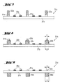
- FIG. 7 shows a variant of that shown in FIG. 4 Mask shown.
- the mask 31a shown in FIG. 7 differs differs from the mask shown in FIG. that marking areas 61a between webs 33a and a membrane layer 37a are arranged.
- the mask 31a can by modification of that described for the mask of FIG. 4 Manufacturing process are manufactured. With such a This is because the process is advantageously carried out before application the membrane layer on the substrate made of the web material an etch-stop layer is applied to this substrate. This serves to etch the webs 33a out of the substrate does not damage the membrane layer by the etching process becomes.
- the etch stop layer is after the etching out Webs 33a removed in a separate step so that the membrane layer 37a is exposed between the webs 33a.
- the embodiment of the invention shown in Figure 6 again has a projection beam cross section 43b, which consists of a rectangular central area 46b and two opposite sides of the central region 46b triangular areas 47b is formed.
- the distance of the The tips of the triangular areas 47b are again selected that it has a clear width between adjacent webs 33b equivalent.
- Projection beam cross section 43b arranged at point O. Hit the beam center of gravity on the predetermined path 49b thus no electrons of the projection beam cross section 43b on the webs 33b.
- the electron beam of FIG. 6 comprises two Positioning auxiliary beams 75, which are on both sides outside of the projection beam 43b are arranged.
- the positioning beams 75 can for example by the in FIG. 4 shows diaphragm device 45 shown schematically are formed together with the projection beam 43b.
- This Auxiliary beams 75 interact with marking areas 61b, which are each arranged centrally on the webs 33b and have a width e that is less than the width c of the webs 33b of, for example, 200 ⁇ m.
- marking areas 61b which are each arranged centrally on the webs 33b and have a width e that is less than the width c of the webs 33b of, for example, 200 ⁇ m.
- Projection beam cross section 43b hit the auxiliary beams 75 on the area of the end faces of the webs 33b, which are not covered by the marking area 61b.
- the projection beam cross-section differs from that predetermined path by a distance ⁇ y as for the in 6 the lower projection beam cross section 43b Beam center of gravity D is shown, it hits in the Figure 6 right auxiliary beam 75 on the marking area 61b.
- the sensor can be detected by electron optics Correct the position of the projection beam cross-section. The correction is carried out in such a way that the measurement signal of the Sensor is minimized, i.e. such that no electrons of the auxiliary beams 75 fall on the marking areas 61b.
- FIG. 8 A mask that can be used for the embodiment of FIG. 6 31b is shown in cross section in FIG.
- the mask 31b FIG. 8 is similar to the mask shown in FIG. 4, but with the difference that the marking areas 61b do not cover the entire end face of the webs 33b.
- the Mask 31b can be used to manufacture the mask of FIG Similar processes are produced, but in for example a further etching step to form the Marking area 61b used material removed in this way becomes that the marking areas 61b exist with their width e stay.
- FIG. 9 Another embodiment for a mask 31c with marking areas 61c, whose width e is less than one Width c of webs 33c is shown in FIG. 9. That mask is also in one for manufacturing the one in FIG. 4 The mask shown can be used to produce in an additional step the marking areas 61c the membrane layer 37c are deposited.
- FIG. 10 shows a variant of that shown in FIG. 6 Embodiment shown.
- a projection beam cross section also points here 43d a shape such that peaks of triangles 47b when the Beam center of gravity O on a predetermined path 49d webs Do not touch 33d of the mask.
- a positioning beam with its beam cross section 75d in the mask plane is with respect to the projection beam cross section 43d arranged so that when properly positioned projection beam cross section 43d Part of the auxiliary beam 75d onto the marking area 61d meets. This leads to an interaction of electrons of the Auxiliary beam 75d with the material of the marking area 61d, which is detected by the sensor and via the energy analyzer as the target measurement signal to the deflection signal generator is fed.
- the deflection generator evaluates the resulting measurement signal and then controls the electron-optical component (reference symbol 57 in Figure 4) such that the measurement signal on a predetermined value is held to the projection beam cross section 73d to position on the predetermined path 49d.
- FIG. 11 shows a further embodiment of the invention shown. This is the embodiment shown in FIG. 10 very similar, but here is a marking area 61e together with a positioning auxiliary beam 75e not only for positioning the beam center of gravity O des Projection beam cross section 43e on a predetermined one Lane 49e used. Auxiliary beam 75e and marking area 61e are still used here to achieve of the end point 53e (see FIG. 3) during the movement of the projection beam 43e along the predetermined path 49e determine.
- the end point 53e is at a distance g from a crosspiece 35e arranged, the distance of the beam center of gravity O from a front front 77 of the projection beam cross section 43e equivalent.
- the marking area 61e extends along the web 33e towards the crosspiece 35e, but ends with a distance in front of the web 35e, which is also the distance g corresponds in such a way that when the projection beam center of gravity is arranged O at the end point 53e just none Overlap between the auxiliary beam 75e and the marking area 61e takes place.
- the number of interactions is corresponding between the electrons of the auxiliary beam 75e and the marking area 61e has dropped to zero, which is above the Sensor can be detected and, among other things, as a signal for it can be used to project the projection beam at a Switch off end point 53e of its predetermined path 49e.
- positioning aids 75f In addition to a projection beam 43f, there are two on both sides here positioning aids 75f arranged thereon intended.
- the positioning auxiliary beams 75f run during the movement of the projection beam 43f on the predetermined path 49f on marking strips 61f to pass over the interaction of the electrons of the auxiliary beam 75f with the marking strip 61f the beam center of gravity O on the predetermined path 49f as described above position.
- end markings 79 are attached in such a way that these of the auxiliary beams 75f are hit as soon as the Beam center O approaches the end point 53f.
- the end marks 79 are formed from a material whose interaction interacting with the electron beam with the materials as they differ for the Formation of the webs 33f, 35f, the membrane layer, the scattering areas and the marking layer 61f can be used. However, this interaction is also from the sensor or detectable by a sensor provided separately for this, so that reaching end position 53f is similar to that in FIG Figure 11 illustrated embodiment can be detected.
- FIG. 13 shows a variant of that shown in FIG. 5 Embodiment shown.
- a marking area 61g is not shown in FIG Projection arranged over a web 33g, but in the area between adjacent webs 33g, in such a way that a Projection beam cross section 43g with properly on a predetermined path 49g positioned beam center of gravity O with its transversely to the direction of extension of the web 49g tapered part, that is, with its triangular area 47g, overlapped with the marking strip 61g.
- Changing the overlap area also changes the number the interactions between the electrons of the beam the material of the marking area 61g, which is about the sensor is detected and to correct the path of the beam cross section is used.
- the marking area is arranged between the webs, that is in one Area which is used for the formation of the pattern of the mask Scattering ranges (reference number 39 in FIG. 4) is used, care must be taken here that the scattering of the electrons is so small due to the material of the marking area 61g that disturbing the imaging of the pattern on the substrate is largely avoided. However, there are still enough many interactions that can be detected via the sensor are to correct the beam guidance as before described to perform.
- the two marking areas 61 shown in FIG. 5 it is possible for the two marking areas 61 shown in FIG. 5 to provide different materials that are related distinguish their interaction with the electron beams. This can be done using a suitable sensor or a pair sensors determine whether the center of gravity of the beam of the projection beam 43 to the right or to the left of deviates from its predetermined path 49. Such a mask can be produced by the two materials for the webs 33 can be used alternately, i.e. every second bridge from the the same material is formed.
- FIG. 4 Another variant of the mask shown in Figure 4 can be manufactured in that the marking material for material used in the webs is added, for example by doping or implanting. The bridges thus form even the marking areas.
- FIG. 14 shows a further variant of that in FIGS. 7, 8 and 9 masks shown schematically.
- the FIG. 14 shows the mask 31h that differs from that in FIGS previous masks shown essentially in that a marking area 61h, seen in projection in the beam direction, not overlapped with a web 33h, but arranged next to it on a membrane layer 37h is.
- the Area between adjacent marking areas 61h used i.e. an area that is one of the clear width between the marking areas shown in FIG. 14 61h has a corresponding or smaller width.
- This mask can be used together with projection beam cross sections can be used as described above.
- a coordination between the marking areas 61h and the projection beam cross section used be as it was explained in connection with Figure 5.
- the projection beam cross-section has a width that of the clear width between the marking areas 61h equivalent.
- the beam guidance then takes place in such a way that the Detector 65 of Figure 4 is essentially a detection signal Zero detected when the projection beam cross section in its target position with respect to the mask is arranged.
- the Projection beam cross section of laterally arranged auxiliary beams has to generate the signal for the detector 65 are provided and the beam guidance then preferably in such a way that that generated by the detector 65 Measurement signal kept at a predetermined constant value becomes.
- the vote can also take place as described in Was explained in connection with Figure 13, wherein the projection beam cross-section with its tapered sides Areas falls on the marking areas 61h and again the beam is guided in such a way that the detection signal of the detector 65 at a predetermined constant value is held.
- the mask 31h of FIG. 14 also has masking areas 81, which, seen in projection parallel to the particle beam, overlap with the marking areas 61h.
- masking area 81 extend even in projection parallel to the pond jet over the Marking areas 61h out and also overlap with the Bridges 33h.
- the masking areas 81 have the task charged particles passing through the marking areas 61h or the bars 33h were not or only slightly scattered, disperse so far that they are not on the exposure Layer are mapped as is the case for the beam 13 in Figure 1 has been explained.
- the masking areas 81 and the scattering areas 39h can molded in a common manufacturing step, such as this for the scatter ranges in the previously described Embodiment has already been explained.
- 7, 8, 9 and 14 are the masks described with respect to the membrane layer in each case on that of the beam shaping direction facing side attached.
- the marking layer is seen in projection parallel to the particle beam, with the base of the web overlaps, with the marking areas extend over the entire width of the support web can, as in particular in connection with the figures 4 and 7, or where the marking areas have a width that is less than the width of the Support bridges, as is particularly the case in connection with the Figures 8 and 9 has been explained.
- the marking areas can be parallel in projection to the pond jet also arranged next to the support web be, and at a distance from this, as particularly in Was explained in connection with Figure 13, or directly adjacent to this, as in connection with FIG. 14 was explained.
- the scattering areas on the membrane layer on the same side as the webs or on each on the opposite side.
Landscapes
- Engineering & Computer Science (AREA)
- Chemical & Material Sciences (AREA)
- Nanotechnology (AREA)
- Physics & Mathematics (AREA)
- General Physics & Mathematics (AREA)
- Analytical Chemistry (AREA)
- Crystallography & Structural Chemistry (AREA)
- Mathematical Physics (AREA)
- Theoretical Computer Science (AREA)
- Condensed Matter Physics & Semiconductors (AREA)
- Manufacturing & Machinery (AREA)
- Electron Beam Exposure (AREA)
- Measurement Of Radiation (AREA)
Abstract
- eine Membranschicht (37) aus einem ersten Material,
- das Muster bildende Streubereiche (39) aus einem die geladenen Teilchen stärker als die Membranschicht (37) streuenden zweiten Material und
- eine Mehrzahl von sich geradlinig erstreckenden, mit Abstand voneinander angeordneten und die Membranschicht (37) samt der Streubereiche (39) tragenden Stützstegen (33),
- eine Strahlformungseinrichtung (45) zum Erzeugen des Projektionsstrahls (41) mit einem vorbestimmten Projektionsstrahlquerschnitt in der Maskenebene,
- eine Positionier-Bewegungseinrichtung (57,55), um den Projektionsstrahlquerschnitt (43) in der Maskenebene entlang einer vorbestimmten Bahn parallel zu der Erstreckungsrichtung der Stege (33) über die Maske(31) zu bewegen.
Description
- Figur 1
- eine Projektionsvorrichtung gemäß dem Stand der Technik;
- Figur 2
- eine Darstellung einer erfindungsgemäßen Maske in Draufsicht sowie eine Erläuterung von Richtungen der Strahlführung;
- Figur 3
- eine Vergrößerung der Figur 2 zur Erläuterung der Führung eines Projektionsstrahlquerschnitts entlang einer vorbestimmten Bahn;
- Figur 4
- eine erfindungsgemäße Projektionsvorrichtung;
- Figur 5
- eine Darstellung der Anordnung eines bei der Projektionsvorrichtung der Figur 4 verwendeten Projektionsstrahlquerschnitts bezüglich Markierungsbereichen;
- Figur 6
- eine Variante der Erfindung mit Positionierungshilfsstrahl;
- Figur 7
- eine Variante der in Figur 4 dargestellten Maske;
- Figur 8
- eine weitere Ausführungsform der Maske zur Verwendung mit Positionierungshilfsstrahl gemäß Figur 6;
- Figur 9
- eine Variante der Maske zur Verwendung mit Positionierungshilfsstrahl gemäß Figur 6;
- Figur 10
- eine weitere Variante der Erfindung mit Positionierungshilfsstrahl;
- Figur 11
- eine Ausführungsform der Erfindung zum Erfassen eines Bahnendes;
- Figur 12
- eine Variante der in Figur 11 dargestellten Ausführungsform zur Erfassung des Bahnendes und
- Figur 13
- eine Variante der in Figur 5 dargestellten Ausführungsform.
- Figur 14
- eine weitere Variante der in Figur 4 gezeigten Maske.
Claims (26)
- Projektionsvorrichtung zum Abbilden eines Musters einer Maske (31) auf ein mit einer strahlungsempfindlichen Schicht versehenes Substrat mittels eines Strahls projizierter geladener Teilchen,
wobei die Maske (31) aufweist:und wobei die Projektionsvorrichtung umfaßt:eine Membranschicht (37) aus einem ersten Material,das Muster bildende Streubereiche (39) aus einem die geladenen Teilchen stärker als die Membranschicht (37) streuenden zweiten Material undeine Mehrzahl von sich geradlinig erstreckenden, mit Abstand voneinander angeordneten und die Membranschicht (37) samt der Streubereiche (39) tragenden Stützstegen (33),dadurch gekennzeichnet, daß ein Sensor (65) zur Abgabe eines Meßsignals (69) vorgesehen ist, welches von der Anzahl der geladenen Teilchen abhängt, die einen an der Maske (31) vorgesehenen Markierungsbereich (61) treffen.eine Strahlformungseinrichtung (45) zum Erzeugen des Projektionsstrahls mit einem vorbestimmten Projektionsstrahlquerschnitt (43) in der Maskenebene,eine Positionier-Bewegungseinrichtung (57,55), um den Projektionsstrahlquerschnitt (43) in der Maskenebene entlang einer vorbestimmten Bahn (49) parallel zu der Erstreckungsrichtung der Stege (33) über die Maske(31) zu bewegen, - Projektionsvorrichtung nach Anspruch 1, wobei die Positionier-Bewegungseinrichtung (57) auf das Meßsignal (69) anspricht, um Abweichungen Δy von der vorbestimmten Bahn (49) zu reduzieren.
- Projektionsvorrichtung nach einem der Ansprüche 1 bis 2, wobei der Projektionsstrahlquerschnitt (43) in Richtung quer zu der Erstreckungsrichtung der Stege (33) eine Breite aufweist, die im wesentlichen der lichten Weite (d) zwischen benachbarten Stegen (33) entspricht.
- Projektionsvorrichtung nach einem der Ansprüche 1 bis 3, wobei die Strahlformungseinrichtung ferner wenigsten einen zur Wechselwirkung mit dem Markierungsbereich (61) auf der Maske vorgesehenen Positionierungshilfsstrahl erzeugt, dessen Hilfsstrahlquerschnitt (75) in der Maskenebene bezüglich dem Projektionsstrahlquerschnitt (43) mit vorbestimmtem konstanten Abstand angeordnet ist.
- Projektionsvorrichtung nach Anspruch 4, wobei der Hilfsstrahlquerschnitt (75) sich in eine Richtung quer zu einer Erstreckungsrichtung der Bahn (49) des Strahls kontinuierlich verjüngt.
- Projektionsvorrichtung nach Anspruch 4 oder 5, wobei die Strahlformungseinrichtung zwei Positionierungshilfsstrahlen (75) erzeugt, deren Hilfsstrahlquerschnitte in der Maskenebene in Richtung quer zu der Erstreckungsrichtung der Stege (33b) mit einem lichten Abstand voneinander angeordnet sind, der größer ist als die lichte Weite zwischen benachbarten Stegen (33b).
- Projektionsvorrichtung nach einem der Ansprüche 1 bis 6, wobei die Positionier-Bewegungseinrichtung (57) die Bahn des Projektionsstrahlquerschnitts (43) derart steuert, daß die Anzahl der den Markierungsbereich (61) treffenden geladenen Teilchen minimiert ist.
- Projektionsvorrichtung nach einem der Ansprüche 1 bis 6, wobei die Positionier-Bewegungseinrichtung (57) die Bahn des Projektionsstrahlquerschnitts (43) derart steuert, daß die Anzahl der die Markierungsbereiche (61) treffenden geladenen Teilchen einem vorbestimmten Wert entspricht.
- Projektionsvorrichtung nach Anspruch 1, wobei die Positionier-Bewegungseinrichtung (57) auf das Meßsignal anspricht, um die Bewegung des Projektionsstrahlquerschnitts (43) entlang der Bahn (49) zu beenden.
- Maske für eine Projektionsvorrichtung zum Abbilden eines Musters der Maske auf ein mit einer strahlungsempfindlichen Schicht versehenes Substrat mittels eines Strahls projizierter geladener Teilchen, wobei die Maske (31) umfaßt:gekennzeichnet durch wenigstens einen durch ein Markierungsmaterial gebildeten Markierungsbereich (61), wobei sich das Markierungsmaterial hinsichtlich seiner Wechselwirkung mit den geladenen Teilchen von dem ersten und dem zweiten Material unterscheidet und diese Wechselwirkung mittels eines Sensors (65) nachweisbar ist.eine Membranschicht (37) aus einem ersten Material,das Muster bildende Streubereiche (39) aus einem die geladenen Teilchen stärker als die Membranschicht (37) streuenden zweiten Material undeine Mehrzahl von mit Abstand voneinander angeordneten und die Membranschicht (37) samt der Streubereiche (39) tragenden Stützstegen (33),
- Maske nach Anspruch 10, wobei das Markierungsmaterial eine andere Streuwirkung oder/und eine andere Reflexionswirkung oder/und eine andere Absorptionswirkung für die geladenen Teilchen aufweist als das erste und das zweite Material.
- Maske nach Anspruch 10 oder 11, wobei die Wechselwirkung mittels eines Auger-Elektronendetektors oder/und eines Rückstreuelektronendetektors oder/und eines Röntgenstrahlungsdetektors (65) oder/und eines Fluoreszenzstrahlungsdetektors nachweisbar ist.
- Maske nach einem der Ansprüche 10 bis 12, wobei der Markierungsbereich (61) durch eine auf eine von der Membranschicht (37) abgewandten Stirnseite des Stegs (33) aufgebrachte Schicht aus dem dritten Material gebildet ist.
- Maske nach einem der Ansprüche 10 bis 12, wobei der Markierungsbereich (61a) durch eine zwischen der Membranschicht (37a) und dem Steg (33) angeordnete Markierungsschicht aus dem dritten Material gebildet ist.
- Maske nach einem der Ansprüche 10 bis 12, wobei der Markierungsbereich (61c) durch eine auf der dem Steg (33c) abgewandten Seite der Membranschicht (37c) angeordnete Markierungsschicht aus dem dritten Material gebildet ist.
- Maske nach einem der Ansprüche 10 bis 15, wobei sich der Markierungsbereich (61) parallel zu einem diesem zugeordneten Steg (33) erstreckt.
- Maske nach Anspruch 16, wobei der Markierungsbereich (61) durch den Steg (33) gebildet ist.
- Maske nach einem der Ansprüche 10 bis 17, wobei der Markierungsbereich(33), gesehen in Projektion parallel zu dem Teilchenstrahl(41), mit der projizierten Fläche des Stegs (33) zusammenfällt.
- Maske nach einem der Ansprüche 10 bis 18, wobei der Markierungsbereich (61), gesehen in Projektion parallel zu dem Teilchenstrahl (41), innerhalb der projizierten Fläche des Stegs (33) und mit einem vorbestimmten Abstand von deren Rändern angeordnet ist.
- Maske nach einem der Ansprüche 10 bis 19, wobei der Markierungsbereich (61g), gesehen in Projektion parallel zu dem Teilchenstrahl, außerhalb der projizierten Fläche des Stegs (33) angeordnet ist.
- Maske nach Anspruch 20, wobei der Markierungsbereich mit einem vorbestimmten Abstand von den Rändern des Stegs angeordnet ist.
- Maske nach einem der Ansprüche 10 bis 21, wobei wenigstens ein Maskierungsbereich (81) vorgesehen ist, der, gesehen in Projektion parallel zu dem Teichenstrahl, mit dem Markierungsbereich (61h) wenigstens teilweise überlappt und der aus einem geladene Teilchen stärker als die Membranschicht (37h) oder/und das Markierungsmaterial oder/und der Stützsteg (33h) streuenden Material gebildet ist.
- Maske nach Anspruch 22, wobei das Material des Maskierungsbereichs (81) das Mateial des Streubereichs 39h umfasst.
- Maske nach einem der Ansprüche 10 bis 23, wobei das Markierungsmaterial zwei verschiedene Markierungsmaterialien mit unterscheidbarer Wechselwirkung umfaßt,
wobei benachbarten Stegen jeweils paarweise verschiedene Markierungsmaterialien zugeordnet sind. - Verfahren zur Belichtung einer strahlungsempfindlichen Schicht mittels durch eine Maske projizierter geladener Teilchen, umfassend die Schritte:Bereitstellen einer Maske gemäß einem der Ansprüche 10 bis 24,Bereitstellen einer Projektionsvorrichtung gemäß einem der Ansprüche 1 bis 9, undErzeugen des Projektionsstrahls und Bewegen von dessen vorbestimmten Projektionsstrahlquerschnitt in der Maskenebene parallel zur Erstreckungsrichtung der Stege wenigstens in Abhängigkeit von dem Meßsignal derart, daß die Anzahl der die Markierungsbereich treffenden geladenen Teilchen minimiert ist oder einem vorbestimmten Wert entspricht.
- Verfahren zur Belichtung einer strahlungsempfindlichen Schicht mittels durch eine Maske projizierter geladener Teilchen, umfassend die Schritte:Bereitstellen einer Maske gemäß einem der Ansprüche 10 bis 24,Bereitstellen einer Projektionsvorrichtung gemäß einem der Ansprüche 1 bis 9,Erzeugen des Projektionsstrahls und Bewegen von dessen vorbestimmten Projektionsstrahlquerschnitts in der Maskenebene parallel zur Erstreckungsrichtung der Stege, undBeenden der Bewegung wenigstens in Abhängigkeit von dem Meßsignal.
Applications Claiming Priority (2)
| Application Number | Priority Date | Filing Date | Title |
|---|---|---|---|
| DE10041040 | 2000-08-22 | ||
| DE10041040A DE10041040A1 (de) | 2000-08-22 | 2000-08-22 | Vorrichtung und Verfahren zur Belichtung einer strahlungsempfindlichen Schicht mittels geladener Teilchen sowie Maske hierfür |
Publications (3)
| Publication Number | Publication Date |
|---|---|
| EP1182505A2 true EP1182505A2 (de) | 2002-02-27 |
| EP1182505A3 EP1182505A3 (de) | 2004-02-04 |
| EP1182505B1 EP1182505B1 (de) | 2006-09-27 |
Family
ID=7653290
Family Applications (1)
| Application Number | Title | Priority Date | Filing Date |
|---|---|---|---|
| EP01120080A Expired - Lifetime EP1182505B1 (de) | 2000-08-22 | 2001-08-21 | Vorrichtung und Verfahren zur Belichtung einer strahlungsempfindlichen Schicht mittels geladener Teilchen sowie Maske hierfür |
Country Status (6)
| Country | Link |
|---|---|
| US (1) | US7015487B2 (de) |
| EP (1) | EP1182505B1 (de) |
| JP (1) | JP2002134404A (de) |
| KR (1) | KR100838258B1 (de) |
| DE (2) | DE10041040A1 (de) |
| TW (1) | TW588226B (de) |
Families Citing this family (5)
| Publication number | Priority date | Publication date | Assignee | Title |
|---|---|---|---|---|
| JP4738723B2 (ja) * | 2003-08-06 | 2011-08-03 | キヤノン株式会社 | マルチ荷電粒子線描画装置、荷電粒子線の電流の測定方法及びデバイス製造方法 |
| JP2006208104A (ja) * | 2005-01-26 | 2006-08-10 | Toyo Ink Mfg Co Ltd | 電子線照射装置および電子線照射方法 |
| KR100972991B1 (ko) * | 2009-12-10 | 2010-07-30 | 주식회사 이젠 | 승하강조류를 갖도록 하는 오탁방지장치 |
| WO2013112586A1 (en) | 2012-01-24 | 2013-08-01 | Smith & Nephew, Inc. | Porous structure and methods of making same |
| JP5662393B2 (ja) * | 2012-08-30 | 2015-01-28 | 株式会社アドバンテスト | 電子ビーム検出器、電子ビーム処理装置及び電子ビーム検出器の製造方法 |
Family Cites Families (35)
| Publication number | Priority date | Publication date | Assignee | Title |
|---|---|---|---|---|
| US4521711A (en) * | 1982-04-14 | 1985-06-04 | Clarion Co., Ltd. | Unidirectional transducer for a surface-acoustic-wave device and a method of making same |
| US4736172A (en) * | 1984-09-03 | 1988-04-05 | Siemens Aktiengesellschaft | Transducer for SAW arrangements |
| US4910839A (en) * | 1984-12-03 | 1990-03-27 | R.F. Monolithics, Inc. | Method of making a single phase unidirectional surface acoustic wave transducer |
| AT393925B (de) * | 1987-06-02 | 1992-01-10 | Ims Ionen Mikrofab Syst | Anordnung zur durchfuehrung eines verfahrens zum positionieren der abbildung der auf einer maske befindlichen struktur auf ein substrat, und verfahren zum ausrichten von auf einer maske angeordneten markierungen auf markierungen, die auf einem traeger angeordnet sind |
| US5130213A (en) * | 1989-08-07 | 1992-07-14 | At&T Bell Laboratories | Device manufacture involving lithographic processing |
| US5079112A (en) * | 1989-08-07 | 1992-01-07 | At&T Bell Laboratories | Device manufacture involving lithographic processing |
| US5258246A (en) * | 1989-08-07 | 1993-11-02 | At&T Bell Laboratories | Device manufacture involving lithographic processing |
| US5264751A (en) * | 1989-10-20 | 1993-11-23 | Thomson-Csf | Unilateral surface wave transducer |
| US5073763A (en) * | 1990-11-02 | 1991-12-17 | R.F. Monolithics, Inc. | Group single-phase unidirectional transducers with 3/8λand 5/8λ sampling |
| US5162689A (en) * | 1991-05-01 | 1992-11-10 | Motorola, Inc. | Single-phase uni-directional acoustic wave transducer |
| JP2844968B2 (ja) * | 1991-06-27 | 1999-01-13 | 日本電気株式会社 | 弾性表面波フィルタ用重み付け電極 |
| US5260151A (en) * | 1991-12-30 | 1993-11-09 | At&T Bell Laboratories | Device manufacture involving step-and-scan delineation |
| US5287036A (en) * | 1992-03-02 | 1994-02-15 | Motorola, Inc. | Method and apparatus for acoustic wave inductance |
| US5376505A (en) * | 1992-03-16 | 1994-12-27 | At&T Corp. | Device fabrication entailing submicron imaging |
| US5316879A (en) * | 1992-07-14 | 1994-05-31 | At&T Bell Laboratories | Sub-micron device fabrication using multiple aperture filter |
| US5334960A (en) * | 1993-02-16 | 1994-08-02 | Motorola, Inc. | Conjugately matched acoustic wave transducers and method |
| US5353206A (en) * | 1993-06-21 | 1994-10-04 | Fejes James M | In-ground storage container |
| US5406159A (en) * | 1993-11-11 | 1995-04-11 | Rf Monolithics, Inc. | Surface acoustic wave gratings having selected reflectivity |
| EP0669636A1 (de) * | 1994-02-25 | 1995-08-30 | AT&T Corp. | Fehlerwahrnehmung in einen Herstellungssystem |
| JP3606944B2 (ja) * | 1994-04-25 | 2005-01-05 | ノキア コーポレイション | Sawフィルタ |
| US5650629A (en) * | 1994-06-28 | 1997-07-22 | The United States Of America As Represented By The Secretary Of The Air Force | Field-symmetric beam detector for semiconductors |
| DE69522066T2 (de) * | 1994-09-28 | 2002-03-28 | Ngk Insulators, Ltd. | Akustische Oberflächenwellenanordnung |
| US5648188A (en) * | 1995-06-07 | 1997-07-15 | International Business Machines Corporation | Real time alignment system for a projection electron beam lithographic system |
| JPH11142121A (ja) * | 1997-11-11 | 1999-05-28 | Nikon Corp | レチクルの歪み計測方法および歪み計測装置 |
| US6147574A (en) * | 1997-11-20 | 2000-11-14 | Murata Manufacturing Co., Ltd. | Unidirectional surface acoustic wave transducer and transversal-type saw filter having the same |
| US5973826A (en) * | 1998-02-20 | 1999-10-26 | Regents Of The University Of California | Reflective optical imaging system with balanced distortion |
| US5985493A (en) * | 1998-04-08 | 1999-11-16 | Lucent Technologies Inc. | Membrane mask for projection lithography |
| JPH11307445A (ja) * | 1998-04-23 | 1999-11-05 | Nikon Corp | 荷電粒子線露光装置及びその投影マスク |
| US6051346A (en) * | 1998-04-29 | 2000-04-18 | Lucent Technologies Inc. | Process for fabricating a lithographic mask |
| US6142641A (en) * | 1998-06-18 | 2000-11-07 | Ultratech Stepper, Inc. | Four-mirror extreme ultraviolet (EUV) lithography projection system |
| EP0969326B1 (de) | 1998-07-01 | 2012-10-17 | ASML Netherlands B.V. | Lithographischer Apparat |
| TW530189B (en) * | 1998-07-01 | 2003-05-01 | Asml Netherlands Bv | Lithographic projection apparatus for imaging of a mask pattern and method of manufacturing a device using a lithographic projection apparatus |
| US6177218B1 (en) * | 1998-08-07 | 2001-01-23 | Lucent Technologies Inc. | Lithographic process for device fabrication using electron beam imaging |
| US6040095A (en) * | 1998-09-30 | 2000-03-21 | Nikon Corporation | Measurement marks for e-beam projection mask and method of using |
| US6033079A (en) * | 1999-03-15 | 2000-03-07 | Hudyma; Russell | High numerical aperture ring field projection system for extreme ultraviolet lithography |
-
2000
- 2000-08-22 DE DE10041040A patent/DE10041040A1/de not_active Withdrawn
-
2001
- 2001-08-15 JP JP2001246372A patent/JP2002134404A/ja active Pending
- 2001-08-21 EP EP01120080A patent/EP1182505B1/de not_active Expired - Lifetime
- 2001-08-21 TW TW090120470A patent/TW588226B/zh not_active IP Right Cessation
- 2001-08-21 US US09/934,262 patent/US7015487B2/en not_active Expired - Fee Related
- 2001-08-21 DE DE50111076T patent/DE50111076D1/de not_active Expired - Lifetime
- 2001-08-22 KR KR1020010050792A patent/KR100838258B1/ko not_active Expired - Fee Related
Also Published As
| Publication number | Publication date |
|---|---|
| KR20020015673A (ko) | 2002-02-28 |
| DE10041040A1 (de) | 2002-03-07 |
| KR100838258B1 (ko) | 2008-06-17 |
| TW588226B (en) | 2004-05-21 |
| US20020071996A1 (en) | 2002-06-13 |
| JP2002134404A (ja) | 2002-05-10 |
| US7015487B2 (en) | 2006-03-21 |
| DE50111076D1 (de) | 2006-11-09 |
| EP1182505B1 (de) | 2006-09-27 |
| EP1182505A3 (de) | 2004-02-04 |
Similar Documents
| Publication | Publication Date | Title |
|---|---|---|
| DE69233067T2 (de) | Integrierte Schaltungen | |
| DE102005046973B4 (de) | Struktur und Verfahren zum gleichzeitigen Bestimmen einer Überlagerungsgenauigkeit und eines Musteranordnungsfehlers | |
| DE19848070B4 (de) | Niedrigenergie-Elektronenstrahllithographie | |
| DE69727112T2 (de) | Elektronenstrahl-Belichtungsgerät und Belichtungsverfahren | |
| EP0027497A2 (de) | Projektionssystem für Korpuskularstrahlen | |
| EP0043863A1 (de) | Verfahren zur Kompensation des Proximity Effekts bei Elektronenstrahl-Projektionsanlagen | |
| DE3224462C2 (de) | ||
| DE112004000395T5 (de) | Halbleiterwafer mit nichtrechteckig geformten Chips | |
| DE69611218T2 (de) | Elektronenquelle für ein Mehrstrahl-Elektronenlithographie-System | |
| DE19510449B4 (de) | Retikel | |
| DE10212931A1 (de) | Brennweiten-Überwachungsverfahren, Brennweiten-Überwachungssystem und Vorrichtungsherstellungsverfahren | |
| EP1182505B1 (de) | Vorrichtung und Verfahren zur Belichtung einer strahlungsempfindlichen Schicht mittels geladener Teilchen sowie Maske hierfür | |
| DE19544753C2 (de) | Elektronenstrahl-Schreibverfahren | |
| DE102015109529B4 (de) | Belichtungsvorrichtung | |
| DE102021119008A1 (de) | Verfahren zur Defekterkennung in einer Halbleiterprobe bei Probenbildern mit Verzeichnung | |
| DE102013108876B4 (de) | Fotolithografisches Verfahren zur Herstellung einer Struktur in einem Strahlung emittierenden Halbleiterbauelement | |
| DE10109965A1 (de) | Teilchenoptische Linsenanordnung und Verfahren unter Einsatz einer solchen Linsenanordnung | |
| DE10295952T5 (de) | Maske, Verfahren zum Herstellen derselben sowie Verfahren zum Herstellen eines Halbleiterbauteils | |
| DE102017203246A1 (de) | Verfahren zur Korrektur eines Spiegels für den Wellenlängenbereich von 5 nm bis 20 nm | |
| DE102018217199A1 (de) | Gitterstruktur für eine diffraktive Optik | |
| DE2755399C2 (de) | ||
| DE102021213160B4 (de) | Verfahren und Vorrichtungen zur Untersuchung und/oder Bearbeitung eines Objekts für die Lithographie | |
| EP1488193B1 (de) | Vorrichtung und verfahren zur maskenlosen afm mikrolithographie | |
| DE69416941T2 (de) | Gerät zur Musteraufzeichnung mittels Elektronenstrahl und Mustersaufzeichnungsverfahren unter Verwendung eines solchen Geräts | |
| DE602005005867T2 (de) | Maske, Belichtungsverfahren sowie Herstellungsverfahren von Halbleiterelementen |
Legal Events
| Date | Code | Title | Description |
|---|---|---|---|
| PUAI | Public reference made under article 153(3) epc to a published international application that has entered the european phase |
Free format text: ORIGINAL CODE: 0009012 |
|
| AK | Designated contracting states |
Kind code of ref document: A2 Designated state(s): AT BE CH CY DE DK ES FI FR GB GR IE IT LI LU MC NL PT SE TR |
|
| AX | Request for extension of the european patent |
Free format text: AL;LT;LV;MK;RO;SI |
|
| RAP1 | Party data changed (applicant data changed or rights of an application transferred) |
Owner name: CARL ZEISS SMT AG |
|
| PUAL | Search report despatched |
Free format text: ORIGINAL CODE: 0009013 |
|
| AK | Designated contracting states |
Kind code of ref document: A3 Designated state(s): AT BE CH CY DE DK ES FI FR GB GR IE IT LI LU MC NL PT SE TR |
|
| AX | Request for extension of the european patent |
Extension state: AL LT LV MK RO SI |
|
| RIC1 | Information provided on ipc code assigned before grant |
Ipc: 7H 01J 37/304 B Ipc: 7H 01J 37/317 B Ipc: 7G 03F 1/14 A Ipc: 7G 03F 1/16 B |
|
| 17P | Request for examination filed |
Effective date: 20040506 |
|
| 17Q | First examination report despatched |
Effective date: 20040628 |
|
| AKX | Designation fees paid |
Designated state(s): DE FR GB NL |
|
| GRAP | Despatch of communication of intention to grant a patent |
Free format text: ORIGINAL CODE: EPIDOSNIGR1 |
|
| GRAS | Grant fee paid |
Free format text: ORIGINAL CODE: EPIDOSNIGR3 |
|
| GRAA | (expected) grant |
Free format text: ORIGINAL CODE: 0009210 |
|
| AK | Designated contracting states |
Kind code of ref document: B1 Designated state(s): DE FR GB NL |
|
| REG | Reference to a national code |
Ref country code: GB Ref legal event code: FG4D Free format text: NOT ENGLISH |
|
| REF | Corresponds to: |
Ref document number: 50111076 Country of ref document: DE Date of ref document: 20061109 Kind code of ref document: P |
|
| GBV | Gb: ep patent (uk) treated as always having been void in accordance with gb section 77(7)/1977 [no translation filed] |
Effective date: 20060927 |
|
| EN | Fr: translation not filed | ||
| PLBE | No opposition filed within time limit |
Free format text: ORIGINAL CODE: 0009261 |
|
| STAA | Information on the status of an ep patent application or granted ep patent |
Free format text: STATUS: NO OPPOSITION FILED WITHIN TIME LIMIT |
|
| 26N | No opposition filed |
Effective date: 20070628 |
|
| PG25 | Lapsed in a contracting state [announced via postgrant information from national office to epo] |
Ref country code: GB Free format text: LAPSE BECAUSE OF FAILURE TO SUBMIT A TRANSLATION OF THE DESCRIPTION OR TO PAY THE FEE WITHIN THE PRESCRIBED TIME-LIMIT Effective date: 20060927 |
|
| PG25 | Lapsed in a contracting state [announced via postgrant information from national office to epo] |
Ref country code: FR Free format text: LAPSE BECAUSE OF FAILURE TO SUBMIT A TRANSLATION OF THE DESCRIPTION OR TO PAY THE FEE WITHIN THE PRESCRIBED TIME-LIMIT Effective date: 20070525 |
|
| PG25 | Lapsed in a contracting state [announced via postgrant information from national office to epo] |
Ref country code: FR Free format text: LAPSE BECAUSE OF FAILURE TO SUBMIT A TRANSLATION OF THE DESCRIPTION OR TO PAY THE FEE WITHIN THE PRESCRIBED TIME-LIMIT Effective date: 20060927 |
|
| PGFP | Annual fee paid to national office [announced via postgrant information from national office to epo] |
Ref country code: DE Payment date: 20090821 Year of fee payment: 9 Ref country code: NL Payment date: 20090814 Year of fee payment: 9 |
|
| REG | Reference to a national code |
Ref country code: NL Ref legal event code: V1 Effective date: 20110301 |
|
| PG25 | Lapsed in a contracting state [announced via postgrant information from national office to epo] |
Ref country code: NL Free format text: LAPSE BECAUSE OF NON-PAYMENT OF DUE FEES Effective date: 20110301 |
|
| REG | Reference to a national code |
Ref country code: DE Ref legal event code: R119 Ref document number: 50111076 Country of ref document: DE Effective date: 20110301 |
|
| PG25 | Lapsed in a contracting state [announced via postgrant information from national office to epo] |
Ref country code: DE Free format text: LAPSE BECAUSE OF NON-PAYMENT OF DUE FEES Effective date: 20110301 |