EP1179772A2 - Microcomputer with interrupt handling capability - Google Patents
Microcomputer with interrupt handling capability Download PDFInfo
- Publication number
- EP1179772A2 EP1179772A2 EP01119064A EP01119064A EP1179772A2 EP 1179772 A2 EP1179772 A2 EP 1179772A2 EP 01119064 A EP01119064 A EP 01119064A EP 01119064 A EP01119064 A EP 01119064A EP 1179772 A2 EP1179772 A2 EP 1179772A2
- Authority
- EP
- European Patent Office
- Prior art keywords
- command
- memory
- processing unit
- central processing
- microcomputer
- Prior art date
- Legal status (The legal status is an assumption and is not a legal conclusion. Google has not performed a legal analysis and makes no representation as to the accuracy of the status listed.)
- Withdrawn
Links
Images


Classifications
-
- G—PHYSICS
- G06—COMPUTING OR CALCULATING; COUNTING
- G06F—ELECTRIC DIGITAL DATA PROCESSING
- G06F15/00—Digital computers in general; Data processing equipment in general
- G06F15/76—Architectures of general purpose stored program computers
- G06F15/78—Architectures of general purpose stored program computers comprising a single central processing unit
- G06F15/7839—Architectures of general purpose stored program computers comprising a single central processing unit with memory
- G06F15/7842—Architectures of general purpose stored program computers comprising a single central processing unit with memory on one IC chip (single chip microcontrollers)
- G06F15/7846—On-chip cache and off-chip main memory
-
- G—PHYSICS
- G06—COMPUTING OR CALCULATING; COUNTING
- G06F—ELECTRIC DIGITAL DATA PROCESSING
- G06F12/00—Accessing, addressing or allocating within memory systems or architectures
- G06F12/02—Addressing or allocation; Relocation
- G06F12/08—Addressing or allocation; Relocation in hierarchically structured memory systems, e.g. virtual memory systems
- G06F12/0802—Addressing of a memory level in which the access to the desired data or data block requires associative addressing means, e.g. caches
- G06F12/0888—Addressing of a memory level in which the access to the desired data or data block requires associative addressing means, e.g. caches using selective caching, e.g. bypass
-
- G—PHYSICS
- G06—COMPUTING OR CALCULATING; COUNTING
- G06F—ELECTRIC DIGITAL DATA PROCESSING
- G06F9/00—Arrangements for program control, e.g. control units
- G06F9/06—Arrangements for program control, e.g. control units using stored programs, i.e. using an internal store of processing equipment to receive or retain programs
- G06F9/46—Multiprogramming arrangements
- G06F9/48—Program initiating; Program switching, e.g. by interrupt
- G06F9/4806—Task transfer initiation or dispatching
- G06F9/4812—Task transfer initiation or dispatching by interrupt, e.g. masked
Definitions
- the invention relates to a microcomputer including a cache therein and suitable for real-time control.
- a microcomputer In real-time control, a microcomputer is required to carry out interruption handling rapidly and in a certain period of time.
- FIG. 1 is a block diagram of a conventional microcomputer.
- a microcomputer 41 illustrated in FIG. 1 is comprised of a central processing unit (CPU) 42, a bus controller 44 electrically connected to the central processing unit 42 through a data bus 43, a command cache 47 electrically connected to the central processing unit 42 through a command bus 45 and to the bus controller 44 through a connection bus 46, and a memory controller 49 electrically connected to the bus controller 44 through an internal bus 48.
- CPU central processing unit
- bus controller 44 electrically connected to the central processing unit 42 through a data bus 43
- command cache 47 electrically connected to the central processing unit 42 through a command bus 45 and to the bus controller 44 through a connection bus 46
- a memory controller 49 electrically connected to the bus controller 44 through an internal bus 48.
- the memory controller 49 is electrically connected further to an external memory 51 through an external bus 50.
- Program access to the external memory 51 has been conventionally made at a relatively low rate.
- the microcomputer 41 is successful in making program access to the external memory 51 at a relatively high rate by virtue of the command cache 47.
- a cache memory is accompanied with a problem that a lot of miss-hits occur, and hence, a cache memory is not suitable to real-time control.
- the microcomputer 41 has to refill commands from the external memory 51.
- the second problem is that reduction in miss-hits is reciprocal to a chip size.
- a cache memory occupies a large area due to its structure. Hence, if a cache memory includes the command cache 47 having a great capacity, a chip size would be increased, resulting in an increase in fabrication costs.
- Japanese Unexamined Patent Publication No. 3-33955 has suggested a cache memory controller in which what is stored in a main memory to which a central processing unit estimates an access is made is transferred to a cache memory operable at a high rate, and data is transmitted to the central processing unit from the cache memory, ensuring that a gap in an operation rate between the central processing unit and the main memory is compensated for.
- the cache memory controller is comprised of first means for storing information about priority to be assigned to cache data, and a controller which makes the first means to store the information, and selects a cache memory to be abandoned.
- the cache memory controller has a function of causing the controller to refer to the information stored in the first means.
- Japanese Unexamined Patent Publication No. 61-837 has suggested a program overlay-lord system in which a requested program module is read out of an external file by means of a route module and a program loader, and the program module is overlay-lorded into a user program area in an internal memory.
- the internal memory includes a buffer area for always storing a program therein, apart from the user program area.
- the route module requests the program loader to load a program module having a priority
- the program loader loads the designated program module to the user program area from the buffer area. If the designated program module is not stored in the buffer area, the program loader loads the designated program module to the buffer area from the external file, and registers a name of the program module in an index. Thereafter, the program loader loads the program module to the user program area.
- Japanese Unexamined Patent Publication No. 4-195540 has suggested an interruption handling system which switches an operation mode of a command executing unit in response to a request of interruption to a data processing unit.
- the interruption handling system is comprised of an interruption arbitration circuit which, if an interruption level highest among interruption requests is higher than an operation level at which the command executing unit operates, outputs the interruption level as a new operation level, a register file having a context which contains a register set used by the command executing unit for executing a program at a predetermined operation level in each of a plurality of frames, a context table in which a flag indicating whether a context is stored in the register file for each of interruption levels defined by a hardware, and a frame number indicative of a frame in which the context is to be stored are registered, a checking circuit which refers to the context table for inspecting the flag and the frame number both associated with a new operation level transmitted from the interruption arbitration circuit and a present operation level transmitted from the command executing unit, and a context indicator which instructs the command
- Japanese Unexamined Patent Publication No. 8-161176 has suggested a method of restarting a microcomputer system including a microprocessor including a command cache, an external memory storing an OS program, a main memory having a first area for storing an OS program and a user area, and a read only memory storing an IPL program.
- the microcomputer system When the microcomputer system is powered on, the IPL program is made to start, and the OS program is loaded into the main memory for starting up the system. If software trouble occurs while the system is in operation, the OS program resets the system, starts the IPL program, initializes the user area, and then, restarts the system.
- Each of entries of the command cache is provided with a bit for prohibiting exchanging a bit. When the system is powered on, a bit for prohibiting exchanging a certain bit is set, and a line of command for restarting the system is written into the certain entry. While the system is on, the line of command is kept stored in the command cache.
- a central processing unit is capable of receiving a command at a higher rate, and which avoids reduction in a hit rate in a program.
- a microcomputer including (a) a cache, (b) a central processing unit, the cache and the central processing unit both being fabricated in one chip, characterized by (c) a memory storing commands to be executed by the central processing unit, the memory storing interruption handling routine therein.
- the memory is comprised of a random access memory (RAM).
- RAM random access memory
- the first advantage is that it is possible to minimize an interruption response time by storing an interruption handling program which is required to make a quick response in real-time control, into the command memory which may be comprised of a random access memory (RAM).
- RAM random access memory
- the second advantage is that since a program is written into the command memory by switching memory maps, the command memory could readily and quickly rewrite a program without necessity of specific surroundings
- the third advantage is that since the command memory can store a program to which many accesses are made, other than a program which is required to make a quick response, it would be possible to reduce a frequency at which the command cache is used, and hence, it would be possible to avoid an increase in a capacity of the command cache which usually occupies a large area.
- FIG. 1 is a block diagram of a conventional microcomputer.
- FIG. 2 is a block diagram of a microcomputer in accordance with the first embodiment of the present invention.
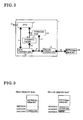
- FIG. 3 illustrates what is stored in each of the memory maps.
- FIG. 4 is a flow chart of a method of initializing the command RAM.
- FIG. 2 is a block diagram of a microcomputer 1 in accordance with the first embodiment of the present invention.
- the microcomputer 1 is comprised of a central processing unit (CPU) 2, a bus controller 4 electrically connected to the central processing unit 2 through a data bus 3, a command cache 7 electrically connected to the central processing unit 2 through a command bus 5, and to the bus controller 4 through a first connection bus 6, a memory controller 9 electrically connected to the bus controller 4 through an internal bus 8, a command random access memory (RAM) 12 electrically connected to the command bus 5 through a second connection bus 10, and to the internal bus 8 through a third connection bus 11, and an external terminal electrically connected to the central processing unit 2.
- CPU central processing unit
- bus controller 4 electrically connected to the central processing unit 2 through a data bus 3
- a command cache 7 electrically connected to the central processing unit 2 through a command bus 5
- to the bus controller 4 through a first connection bus 6
- a memory controller 9 electrically connected to the bus controller 4 through an internal bus 8
- a command random access memory (RAM) 12 electrically connected to the command bus 5 through a second connection bus 10
- the memory controller 9 is electrically connected further to an external memory 15 through an external bus 14.
- the microcomputer 1 having such a structure as mentioned above is a Harvard architecture microcomputer.
- the command RAM 12 stores therein an interruption handling routine which is required to make a quick response.
- the command RAM 12 is initialized by switching memory maps illustrated in FIG. 3.
- the central processing unit 2 can read a command out of the command RAM 12 in one system clock cycle.
- the central processing unit 2 can write a command into the command RAM 12 in one system clock cycle through the data bus 3 and the bus controller 4.
- the central processing unit 2 Since the central processing unit 2 is electrically connected to the command cache 7 through the command bus 5, if the command cache 7 stores a command to be executed by the central processing unit 2, the central processing unit 2 can read a command out of the command cache 7 in one system clock cycle.
- the command cache 7 If the command cache 7 does not store a command to be executed by the central processing unit 2, the command cache 7 carries out a refill operation, specifically, reads commands associated with one line of cache, out of the external memory 15 through the bus controller 4, the internal bus 8, the memory controller 9 and the external bus 14.
- the bus controller 4 exchanges signals on the data bus 3 and the command bus 5 and signals on the internal bus 8 to each other.
- the memory controller 9 exchanges signals on the internal bus 8 and signals on the external bus 14 to each other.
- the central processing unit 2 can read a command out of the external memory 15 in two system clock cycles at least through the command bus 5, the bus controller 4, the internal bus 8, and the memory controller 9, and read data out of and write data into the external memory 15 in two system clock cycles at least through the data bus 3, the bus controller 4, the internal bus 8, and the memory controller 9.
- FIG. 3 illustrates an ordinary memory map (hereinafter, referred to as a first memory map) and a memory map for initializing the command RAM 12 (hereinafter, referred to as a second memory map).
- the command RAM 12 stored in the first memory map is identical to the command RAM 12 stored in the second memory map, through the command RAMs 12 have different addresses from each other.
- the central processing unit 2 When the central processing unit 2 is released from being reset, the central processing unit 2 starts execution of commands from an address of "0000000H". When an interruption occurs, the central processing unit 2 carries out an interruption handling routine designated by an interruption vector table associated with addresses of "0000010H” to "0000480H”, defined in accordance with an interruption request source.
- the command RAM 12 and the external memory 15 are arranged in a memory space, as illustrated in FIG. 3. Specifically, the command RAM 12 is arranged in addresses of "0000000H” to "0100000H", and the external memory 15 is arranged in addresses of "0100000H” and later.
- the central processing unit 2 when the central processing unit 2 is released from being reset, the central processing unit 2 starts execution of commands from an address of "0000000H". Since the address of "0000000H" is assigned to the command Ram 12, the central processing unit 2 reads a command out of the command RAM 12, and executes the thus read-out command.
- the central processing unit 2 executes a program stored in the external memory 15 or the command RAM 12, as follows.
- the central processing unit 2 If the command cache 7 stores a command to be executed by the central processing unit 2, that is, if a cache is hit, the central processing unit 2 reads a command out of the command cache 7, and executes the thus read-out command.
- the central processing unit 2 If the command cache 7 does not store a command to be executed by the central processing unit 2, the central processing unit 2 reads commands associated with a line of cache, out of the external memory 15, and stores the thus read-out commands into the command cache 7. Thereafter, the central processing unit 2 reads the commands out of the command cache 7, and executes the thus read-out commands.
- the central processing unit 2 reads the command out of the command RAM 12, and executes the command.
- the central processing unit 2 branches to the interruption handling routine stored in the addresses of "0000000H” to "0100000H", and starts execution of the interruption handling routine.
- the command RAM 12 is arranged in the addresses of "0000000H” to "0100000H”, and hence, the central processing unit 2 reads a command out of the command RAM 12, and then, executes the interruption handling routine.
- the central processing unit 2 reads a reset routine out of the command RAM 12, and executes the reset routine, immediately after the central processing unit 2 has been reset.
- the command RAM 12 and the external memory 15 are arranged in a memory space, as illustrated in FIG. 3. Specifically, the command RAM 12 is arranged in addresses of "0100000H” to "0200000H”, and the external memory 15 is arranged in addresses of "0000000H” to "0100000H” and addresses of "0200000H” and later.
- the central processing unit 2 when the central processing unit 2 is released from being reset, the central processing unit 2 starts execution of commands from an address of "0000000H". Since the address of "0000000H" is assigned to the external memory 15, the central processing unit 2 reads a command out of the external memory 15, and executes the thus read-out command.
- the microcomputer 1 When the routine for initializing the command RAM 12 is carried out, the microcomputer 1 operates in the same way as a way in which the microcomputer 1 executes an ordinary command stored in the external memory 15 in accordance with the first memory map. That is, the central processing unit 2 executes a program stored in the external memory 15 or the command RAM 12, as mentioned earlier.
- Reset and handling of the external terminal 13 are carried out by an external controller (not illustrated) in steps 100, 101, 103, 104 and 105.
- the second memory map is designated through the external terminal 13 in step 100.
- the central processing unit 2 is released from being reset, in step 101.
- the central processing unit 2 reads a command out of the external memory 15, and executes the thus read-out command, in step 102.
- the above-mentioned programs (a) and (b) are executed in this order, and transfers data (c) and (d) to the addresses of "0100000H” to "0200000H” in which the command RAM 12 is arranged, from the external memory 15, in the initialization routine (b).
- the first memory map is designated through the external terminal 13 in step 104.
- the central processing unit 2 is released from being reset, in step 105.
- the central processing unit 2 reads a command out of the command RAM 12, and executes the thus read-out command, in step 106. Specifically, the reset/interruption vector (c) having been transferred in step 102 and the control program (e) stored in the external memory 15 are executed in this order.
- interruption handling is executed in an order of data (c) and (d) stored in the command RAM 12.
- the microcomputer 1 makes it possible to execute interruption handling rapidly and in a certain period of time, ensuring superior real-time response.
- the central processing unit 2 can receive command more rapidly than the cache memory controller suggested in the above-mentioned Japanese Unexamined Patent Publication No. 3-33955.
- the cache memory controller suggested in the above-mentioned Japanese Unexamined Patent Publication No. 3-33955 was accompanied with a problem that if the command cache was filled with data having high priority, a hit rate in a program was reduced.
- the microcomputer 1 since a command is transferred to the central processing unit 2 through the command RAM 12, even if the command cache 7 is filled with data, in the microcomputer 1 in accordance with the first embodiment, the microcomputer 1 solves the problem of reduction in a hit rate.
- the external terminal 13 is designed to be able to be handled even while the central processing unit 2 is in operation.
- the central processing unit 2 is designed to include an internal register.
- the memory maps were switched through the use of the external terminal 13 in the above-mentioned first embodiment. In contrast, the memory maps are switched by means of the internal register in the third embodiment.
- the internal register may be arranged to initially designate the second memory map after the central processing unit 2 has been released from being reset. Then, after the initialization of the command RAM 12 has been carried out, the first memory map is designated through the internal register in the same manner as the first embodiment.
Landscapes
- Engineering & Computer Science (AREA)
- Theoretical Computer Science (AREA)
- Physics & Mathematics (AREA)
- General Engineering & Computer Science (AREA)
- General Physics & Mathematics (AREA)
- Computer Hardware Design (AREA)
- Software Systems (AREA)
- Memory System Of A Hierarchy Structure (AREA)
- Microcomputers (AREA)
- Memory System (AREA)
Abstract
Description
Claims (11)
- A microcomputer (1) comprising (a) a cache (7), and (b) a central processing unit (2), the cache (7) and the central processing unit (2) both being fabricated in one chip,
characterized by
(c) a memory (12) storing commands to be executed by the central processing unit (2), the memory (12) storing interruption handling routine therein. - The microcomputer (1) as set forth in claim 1, wherein a program is written into the memory (12) by switching memory maps when the microcomputer (1) is turned on.
- The microcomputer (1) as set forth in claim 1, further comprising a bus controller (4) electrically connected to the central processing unit (2) through a first bus (3),the cache (7) being electrically connected to the central processing unit (2) through a second bus (5), and to the bus controller (4) through a third bus (6),the memory (12) being electrically connected to the second bus (5) through a fourth bus (10).
- The microcomputer (1) as set forth in claim 3, further comprising a memory controller (9) electrically connected to the bus controller (4) through a fifth bus (8), to the memory (12) through a sixth bus (11), and to an external memory (15) through a seventh bus (14).
- The microcomputer (1) as set forth in claim 4, wherein the central processing unit (2), if the command cache (7) stores a command to be executed by the central processing unit (2), reads the command out of the command cache (7), and executes the thus read-out command, and if the command cache (7) does not store a command to be executed by the central processing unit (2), reads a command out of the external memory (15), and executes the thus read-out command.
- The microcomputer (1) as set forth in claim 3, wherein the central processing unit (2) reads a command out of the memory (12), and executes the interruption handling routine, when interruption occurs.
- The microcomputer (1) as set forth in claim 3, further comprising an external terminal (13) electrically connected to the central processing unit (2), and wherein a region in which the memory (12) is to be arranged is designated through the external terminal (13).
- The microcomputer (1) as set forth in claim 7, wherein the external terminal (13) can be operated even while the central processing unit (2) is in operation.
- The microcomputer (1) as set forth in claim 3, further comprising an external terminal (13) electrically connected to the central processing unit (2), and wherein memory maps are switched through the external terminal (13).
- The microcomputer (1) as set forth in claim 3, further comprising an internal register, and wherein memory maps are switched by the internal register.
- The microcomputer (1) as set forth in any one of claims 1 to 10, wherein the memory (12) is comprised of a random access memory (RAM).
Applications Claiming Priority (2)
| Application Number | Priority Date | Filing Date | Title |
|---|---|---|---|
| JP2000237996 | 2000-08-07 | ||
| JP2000237996A JP4034032B2 (en) | 2000-08-07 | 2000-08-07 | Microcomputer with built-in cache |
Publications (2)
| Publication Number | Publication Date |
|---|---|
| EP1179772A2 true EP1179772A2 (en) | 2002-02-13 |
| EP1179772A3 EP1179772A3 (en) | 2007-03-21 |
Family
ID=18729765
Family Applications (1)
| Application Number | Title | Priority Date | Filing Date |
|---|---|---|---|
| EP01119064A Withdrawn EP1179772A3 (en) | 2000-08-07 | 2001-08-07 | Microcomputer with interrupt handling capability |
Country Status (3)
| Country | Link |
|---|---|
| US (1) | US7136965B2 (en) |
| EP (1) | EP1179772A3 (en) |
| JP (1) | JP4034032B2 (en) |
Families Citing this family (2)
| Publication number | Priority date | Publication date | Assignee | Title |
|---|---|---|---|---|
| WO2004031963A1 (en) * | 2002-09-30 | 2004-04-15 | Renesas Technology Corp. | Semiconductor data processor |
| BR102014015085B1 (en) † | 2014-05-29 | 2023-11-14 | M.E.P. Macchine Elettroniche Piegatrici S.P.A. | Drawing unit, drawing apparatus and corresponding method |
Family Cites Families (13)
| Publication number | Priority date | Publication date | Assignee | Title |
|---|---|---|---|---|
| JPS5858701B2 (en) | 1978-06-13 | 1983-12-27 | 松下電器産業株式会社 | How to start a microprocessor |
| JPS61837A (en) | 1984-06-13 | 1986-01-06 | Hitachi Ltd | Program overlay loading system |
| JPH0333955A (en) | 1989-06-29 | 1991-02-14 | Nec Corp | Cache memory controller |
| JPH04195540A (en) | 1990-11-28 | 1992-07-15 | Nec Corp | Interruption processing system |
| JPH0528040A (en) | 1991-07-18 | 1993-02-05 | Oki Electric Ind Co Ltd | Quick memory access system |
| US5860099A (en) * | 1993-05-12 | 1999-01-12 | Usar Systems, Inc. | Stored program system with protected memory and secure signature extraction |
| JPH08161176A (en) | 1994-12-05 | 1996-06-21 | Hitachi Ltd | Restart processing method |
| JP3735373B2 (en) | 1995-05-19 | 2006-01-18 | 株式会社ルネサステクノロジ | Microcomputer |
| US5745115A (en) * | 1996-01-16 | 1998-04-28 | International Business Machines Corporation | Graphical user interface having a shared menu bar for opened applications |
| US5961643A (en) * | 1997-09-30 | 1999-10-05 | Micron Electronics, Inc. | Method for attachment or integration of a BIOS device into a computer system using the system memory address and data bus |
| JP3727485B2 (en) * | 1999-04-02 | 2005-12-14 | シャープ株式会社 | Microcomputer with built-in nonvolatile memory |
| JP2001056803A (en) * | 1999-08-19 | 2001-02-27 | Mitsubishi Electric Corp | Microcomputer |
| US6591318B1 (en) * | 2000-01-24 | 2003-07-08 | Micron Technology, Inc. | Computer system having reduced number of bus bridge terminals |
-
2000
- 2000-08-07 JP JP2000237996A patent/JP4034032B2/en not_active Expired - Fee Related
-
2001
- 2001-08-07 EP EP01119064A patent/EP1179772A3/en not_active Withdrawn
- 2001-08-07 US US09/922,950 patent/US7136965B2/en not_active Expired - Fee Related
Also Published As
| Publication number | Publication date |
|---|---|
| JP4034032B2 (en) | 2008-01-16 |
| US20020029322A1 (en) | 2002-03-07 |
| JP2002049607A (en) | 2002-02-15 |
| US7136965B2 (en) | 2006-11-14 |
| EP1179772A3 (en) | 2007-03-21 |
Similar Documents
| Publication | Publication Date | Title |
|---|---|---|
| US9519507B2 (en) | Executing an instruction of currently active thread before context switch upon receiving inactive context ID to be activated | |
| EP1089185A2 (en) | Method of controlling a cache memory to increase an access speed to a main memory, and a computer using the method | |
| US6687763B2 (en) | ATAPI command receiving method | |
| JP4210024B2 (en) | Method of operating storage device and storage device | |
| US7136965B2 (en) | Microcomputer | |
| US20080016296A1 (en) | Data processing system | |
| JP3088303B2 (en) | Cache memory bank controller | |
| JP2002149491A (en) | Processor memory system | |
| JP3991443B2 (en) | Task switching method and data processing apparatus | |
| JP2009258984A (en) | Information processor and load control method | |
| JP3956305B2 (en) | Nonvolatile semiconductor memory device and data processing device | |
| JP2002055822A (en) | Terminal device program control method and method, and recording medium for recording the control program | |
| EP0787326B1 (en) | System and method for processing of memory data and communication system comprising such system | |
| JPH08137753A (en) | Disk cache device | |
| JP2001117819A (en) | Instruction memory circuit and information processing system | |
| JP2001125659A (en) | Information processing device | |
| JP5949330B2 (en) | Information processing apparatus and information processing method | |
| JP2001306335A (en) | Computer | |
| JPH1055308A (en) | Cache memory | |
| JP2002259209A (en) | Arithmetic processing system | |
| US20110099304A1 (en) | Controller and a Method for Controlling the Communication Between a Processor and an External Peripheral Device | |
| JPS6014435B2 (en) | Storage device | |
| JPH10289113A (en) | Saving / restoring method of computer register context | |
| JPS63240649A (en) | Data processor | |
| JPH0320834A (en) | Initial diagnostic method for information processor |
Legal Events
| Date | Code | Title | Description |
|---|---|---|---|
| PUAI | Public reference made under article 153(3) epc to a published international application that has entered the european phase |
Free format text: ORIGINAL CODE: 0009012 |
|
| AK | Designated contracting states |
Kind code of ref document: A2 Designated state(s): AT BE CH CY DE DK ES FI FR GB GR IE IT LI LU MC NL PT SE TR |
|
| AX | Request for extension of the european patent |
Free format text: AL;LT;LV;MK;RO;SI |
|
| RAP1 | Party data changed (applicant data changed or rights of an application transferred) |
Owner name: NEC ELECTRONICS CORPORATION |
|
| PUAL | Search report despatched |
Free format text: ORIGINAL CODE: 0009013 |
|
| AK | Designated contracting states |
Kind code of ref document: A3 Designated state(s): AT BE CH CY DE DK ES FI FR GB GR IE IT LI LU MC NL PT SE TR |
|
| AX | Request for extension of the european patent |
Extension state: AL LT LV MK RO SI |
|
| RIC1 | Information provided on ipc code assigned before grant |
Ipc: G06F 9/445 20060101AFI20011211BHEP |
|
| 17P | Request for examination filed |
Effective date: 20070314 |
|
| 17Q | First examination report despatched |
Effective date: 20070427 |
|
| AKX | Designation fees paid |
Designated state(s): DE FR GB |
|
| STAA | Information on the status of an ep patent application or granted ep patent |
Free format text: STATUS: THE APPLICATION IS DEEMED TO BE WITHDRAWN |
|
| 18D | Application deemed to be withdrawn |
Effective date: 20070908 |