EP1178961B1 - Dispositifs et procedes de collecte de donnees globales durant une inspection de reticule - Google Patents
Dispositifs et procedes de collecte de donnees globales durant une inspection de reticule Download PDFInfo
- Publication number
- EP1178961B1 EP1178961B1 EP00928680.8A EP00928680A EP1178961B1 EP 1178961 B1 EP1178961 B1 EP 1178961B1 EP 00928680 A EP00928680 A EP 00928680A EP 1178961 B1 EP1178961 B1 EP 1178961B1
- Authority
- EP
- European Patent Office
- Prior art keywords
- values
- reticle
- recited
- statistical information
- test
- Prior art date
- Legal status (The legal status is an assumption and is not a legal conclusion. Google has not performed a legal analysis and makes no representation as to the accuracy of the status listed.)
- Expired - Lifetime
Links
Images


Classifications
-
- G—PHYSICS
- G06—COMPUTING; CALCULATING OR COUNTING
- G06T—IMAGE DATA PROCESSING OR GENERATION, IN GENERAL
- G06T7/00—Image analysis
- G06T7/0002—Inspection of images, e.g. flaw detection
- G06T7/0004—Industrial image inspection
- G06T7/001—Industrial image inspection using an image reference approach
-
- G—PHYSICS
- G06—COMPUTING; CALCULATING OR COUNTING
- G06T—IMAGE DATA PROCESSING OR GENERATION, IN GENERAL
- G06T2207/00—Indexing scheme for image analysis or image enhancement
- G06T2207/30—Subject of image; Context of image processing
- G06T2207/30108—Industrial image inspection
- G06T2207/30148—Semiconductor; IC; Wafer
Definitions
- the present invention relates generally to integrated circuit design and fabrication systems. More specifically, the invention relates to mechanisms for inspecting reticles.
- circuit designers provide circuit pattern data, which describes a particular integrated circuit (IC) design, to a reticle production system, or reticle writer.
- the circuit pattern data is typically in the form of a representational layout of the physical layers of the fabricated IC device.
- the representational layout typically includes a representational layer for each physical layer of the IC device (e.g., gate oxide, polysilicon, metallization, etc.), wherein each representational layer is composed of a plurality of polygons that define a layer's patterning of the particular IC device.
- the reticle writer uses the circuit pattern data to write (e.g., typically, an electron beam writer or laser scanner is used to expose a reticle pattern) a plurality of reticles that will later be used to fabricate the particular IC design.
- a reticle inspection system may then inspect the reticle for defects that may have occurred during the production of the reticles.
- a reticle or photomask is an optical element containing at least transparent and opaque regions, and sometimes semi-transparent and phase shifting regions, as well, which together define the pattern of coplanar features in an electronic device such as an integrated circuit.
- Reticles are used during photolithography to define specified regions of a semiconductor wafer for etching, ion implantation, or other fabrication process.
- an optical reticle's features are between about 1 and about 5 times larger than the corresponding features on the wafer.
- exposure systems e.g., x-ray, e-beam, and extreme ultraviolet
- Optical reticles are typically made from a transparent medium such as a borosilicate glass or quartz plate on which is deposited an opaque and/or semi-opaque layer of chromium or other suitable material.
- a transparent medium such as a borosilicate glass or quartz plate on which is deposited an opaque and/or semi-opaque layer of chromium or other suitable material.
- other mask technologies are employed for direct e-beam exposure (e.g., stencil masks), x-ray exposure (e.g., absorber masks), etc.
- the reticle pattern may be created by a laser or an e-beam direct write technique, for example, both of which are widely used in the art.
- each reticle is typically inspected by illuminating it with light emanating from a controlled illuminator.
- a test image of a portion of the reticle is constructed based on the portion of the light reflected, transmitted, or otherwise directed to a light sensor.
- Such inspection techniques and apparatus are well known in the art and are embodied in various commercial products such as many of those available from KLA-Tencor Corporation of San Jose, California.
- the test image of the reticle is typically compared to a baseline image.
- the baseline image is either generated from the circuit pattern data or from an adjacent die on the reticle itself.
- the test image features are analyzed and compared with corresponding features of the baseline image.
- features of the baseline image That is, an edge position within the test image is subtracted from a corresponding edge position within the baseline image to calculate a difference value.
- Each difference value is then compared with a predetermined threshold value. If the test image feature varies from the baseline feature by more than the predetermined threshold, a defect is defined and an error is reported.
- An error report for a particular test image will typically only include a list of errors that were detected within the particular test image and corresponding reticle (e.g., the location of each error and a small image of that defect).
- the list represents the features within the test image that varied from the baseline image by more than the predetermined threshold.
- the list represents the edge positions within the test image that varied more than the predetermined threshold from the corresponding edge positions of the baseline image, as well as any extra or missing features.
- a user of the reticle may wish to know the actual measured values of particular characteristics of features (i. e., edge position) within the test image as a function of position on the reticle. Additionally, the user may wish to know other measurable values of other characteristics (e.g., line width and corner rounding values). By way of another example, the user may wish to know the amount of variance between the features of the test image and the features of the baseline image as a function of position on the reticle.
- variance values may not be large enough to be defined as errors, they may be useful in process control and/or monitoring. Additionally, statistical information of measurable characteristics as a function of position on the reticle, for example, may be used to increase the sensitivity of the inspection process itself, among other applications. That is, the threshold may be adjusted for certain areas of the reticle that typically have more errors than other areas of the reticle.
- US5655110 describes a method of collecting statistical data from a limited number of features from a processed wafer, extrapolating that data to predict the affect of processing across the entire wafer and applying the data to a simulator to ascertain which process steps will bring the actual processed wafer into line with a desired wafer tolerance.
- inspection apparatus and techniques for improving and enhancing information that is output from the inspection procedure are needed. More specifically, inspection mechanisms for providing statistical information about measured characteristics of the reticle are needed.
- the present invention provides a method of inspecting a reticle defining a circuit layer pattern that is used within a corresponding semiconductor process to generate corresponding patterns on a semiconductor wafer, the method comprising: (a) providing a test image of the reticle, the test image having a plurality of test characteristic values; (b) providing a baseline image containing an expected pattern of the test image, the baseline image having a plurality of baseline characteristic values that correspond to the test characteristic values; (c) comparing the test characteristic values to the baseline characteristic values such that a plurality of difference values are calculated for each pair of test and baseline characteristic values; and (d) collecting statistical information characterised in that: the statistical information is collected as the test characteristic values are compared to the baseline characteristic values for the plurality of test characteristic values, wherein the statistical information includes an average or median value of the plurality of test characteristic values or of the difference values.
- test image As each feature or region of a test image of a portion of a reticle is evaluated, statistical information can be collected for the entire test image. That is, as features of the test image are compared to features of the baseline image, measured characteristic values of the test image (or difference values between the test and baseline images) are collected. The collected measured or difference values may be correlated to a number of reticle parameters, such as a reticle position, a particular area on the reticle, a feature density value of a particular area of the reticle, or a process associated with the reticle under test. A count of the measured characteristic or difference values may also be collected. This collected data (e.g., the count and measured values or difference values) may then be used to compute other statistical parameters, such as standard deviation, minimum, maximum, range (maximum minus minimum), and median or average values.
- reticle parameters such as a reticle position, a particular area on the reticle, a feature density value of a particular area of the reticle, or a
- the method of inspecting a reticle defining a circuit layer pattern can be used within a corresponding semiconductor process to generate corresponding patterns on a semiconductor wafer is disclosed.
- a test image of the reticle is provided, and the test image has a plurality of test characteristic values.
- a baseline image containing an expected pattern of the test image is also provided.
- the baseline image has a plurality of baseline characteristic values that correspond to the test characteristic values.
- the test characteristic values are compared to the baseline characteristic values such that a plurality of difference values are calculated for each pair of test and baseline characteristic values. Statistical information is also collected.
- the statistical information can include a second plurality of test characteristics values that are of a different type of characteristic than the first plurality of test characteristic values that are compared to the baseline characteristic values.
- the statistical information may also include a standard deviation value of the second test characteristic values, a median value of the second test characteristic values, and/or an average value of the second test characteristic values.
- the first test characteristic values may be in the form of edge position values and the second test characteristic values include line width values, corner rounding values, transmission values, gate line width values, contact area values, and/or misalignment values.
- the method of monitoring or adjusting a reticle process can be used to generate reticles.
- the method includes (a) generating a first reticle using a reticle process; (b) providing a test image of the first reticle, wherein the test image has a plurality of test characteristic values; (c) providing a baseline image containing an expected pattern of the test image, wherein the baseline image has a plurality of baseline characteristic values that correspond to a first subgroup of the test characteristic values; (d) comparing the first subgroup of test characteristic values to the corresponding baseline characteristic values such that a plurality of difference values are calculated for each pair of test and baseline characteristic values; (e) collecting statistical information based on a second subgroup of the test characteristic values of the first reticle; and(f) adjusting a process parameter of the reticle process if the statistical information indicates that the second subgroup of test characteristic values deviate from the baseline values by more than a predetermined amount.
- the first subgroup can be equal to the second subgroup of test characteristic values.
- the above operations (a) through (e) are repeated for a second reticle.
- the statistical information for the second reticle is compared to the statistical information for the first reticle, and a process parameter of the reticle process is adjusted if the statistical information for the second reticle varies from the statistical information for the first reticle by more than a second predetermined amount.
- the process parameter of the reticle process is adjusted so as to reduce variations in the second subgroup of test characteristic values as a function of reticle position.
- a reticle defining a circuit layer pattern and statistical information about selected characteristic values of the circuit layer pattern can be provided.
- a circuit layer on a semiconductor wafer is generated using the reticle in a photolithography process.
- the resulting circuit layer is inspected based at least in part on the statistical information.
- a second aspect of the present invention provides a computer readable medium containing program instructions for inspecting a reticle defining a circuit layer pattern that is used within a corresponding semiconductor process to generate corresponding patterns on a semiconductor wafer, the computer readable medium storing: (a) computer readable code for providing a test image of the reticle, the test image having a plurality of test characteristic values; (b) computer readable code for providing a baseline image containing an expected pattern of the test image, the baseline image having a plurality of baseline characteristic values that correspond to the test characteristic values; (c) computer readable code for comparing the test characteristic values to the baseline characteristic values such that a plurality of difference values are calculated for each pair of test and baseline characteristic values; and, (d) computer readable code for collecting statistical information characterised in that: the computer readable code for collecting the statistical information is configured to collect the statistical information as the test characteristic values are compared to the baseline characteristic values for a plurality of characteristic values of the test image, wherein the statistical information includes an average or median value of a pluralit
- the computer readable medium can include computer code for collecting statistical information based on the plurality of test characteristic values of the first reticle, adjusting a process parameter of the reticle process if the statistical information indicates that the test characteristic values deviate from the baseline characteristic values by more than a predetermined amount.
- FIG. 1 is a flowchart illustrating an integrated circuit design process 100 in accordance with one embodiment of the present invention.
- an integrated circuit (IC) device is designed using any suitable design techniques.
- EDA electronic design automation
- the IC designer may create the IC device or part of the IC device from scratch with the aid of any suitable design system, such as conventional computer aided design (CAD) tools.
- CAD computer aided design
- the IC designer may use a schematic CAD tool to plan the logic diagrams for a particular IC device.
- the IC designer may write a description of the IC device or portions of the IC device with the aid of a hardware design language, such as VHDL.
- the IC designer generates a circuit pattern database (commonly referred to as a "layout") from the IC design in operation 104.
- the circuit pattern database is composed of a plurality of electronic representations of layout patterns for IC layers that are later converted into a plurality of reticles that are used to fabricate a plurality of physical layers of an IC device. Each physical layer of the fabricated IC device corresponds to one of the reticles and an associated one of the electronic representations of the circuit pattern database.
- one electronic representation may correspond to a diffusion pattern on a silicon substrate, another to a gate oxide pattern, another to a gate polysilicon pattern, another to a contact pattern on an interlayer dielectric, another to a line pattern on a metallization layer, and so on.
- Each electronic representation is composed of a plurality of polygons or other shapes (herein, referred to as "figures"), which together define the reticle pattern.
- the circuit pattern database may be generated using any suitable technique, for example, by using EDA or CAD tools.
- the IC designer may manually lay out the circuit patterns for the IC device with or without preexisting library cells.
- a synthesis tool may automatically create circuit patterns for the IC device from scratch or by piecing together preexisting library cells.
- Each reticle corresponds to one or more electronic representation(s) from the circuit pattern database.
- a reticle is then inspected in operation 108, and it is determined whether the reticle passes inspection in operation 110. If the reticle passes inspection, the reticle may then be used to fabricate a physical layer of the IC device in operation 112. However, if the reticle does not pass inspection, the reticle is either repaired or remade in operation 114, and the new reticle is inspected in operation 108. Operations 106 through 112 may be implemented for some or all of the electronic representations of the circuit pattern database.
- the present invention may be implemented on any suitable inspection tools.
- a KLA 301, 351, or 353UV Reticle Inspection Tool commercially available from KLA-Tencor of San Jose, California, may be employed.
- KLA-Tencor of San Jose, California
- One embodiment of an inspection system is described below in reference to Figure 8 .
- FIG. 2 is a flowchart illustrating the operation 108 of Figure 1 of evaluating the fabricated reticle in accordance with one embodiment of the present invention.
- a baseline image of the reticle may be generated or "rendered" from the provided circuit pattern database.
- the baseline image may be generated in any suitable manner, such as by merely directly converting the contents of the circuit pattern database into an image.
- the circuit pattern database may be rendered by simulating fabrication results from making a reticle that perfectly matches the circuit pattern database. For example, the corners of a circuit pattern in the baseline image may be rounded to account for corner rounding that commonly occurs during fabrication of a reticle.
- the baseline image may also include simulated optical effects from retrieving an optical image of the simulated reticle. Such optical effects are necessarily encountered when an optical inspection technique is used to evaluate a reticle.
- the baseline image may be generated from an adjacent die of the reticle in a die-to-die inspection approach.
- the images of two supposedly identical patterns on a reticle are generated, one for a baseline image and one for a test image described below. Note that many reticles contain the layout patterns of multiple identical (and adjacent) die.
- the reticle is inspected to obtain a test image of the reticle or a portion of the reticle under analysis in operation 604.
- Any suitable mechanism may be implemented for obtaining the test image. For example, an optical or ebeam image be obtained.
- Figure 3 is a flowchart illustrating the operation 606 of Figure 2 of comparing the baseline and test images in accordance with one embodiment of the present invention.
- the test image may be divided into a plurality of regions (herein referred to as "patches") that are analyzed separately during the inspection process.
- Each patch may be any suitable size for efficiently analyzing the test image. For example, processing resources may be limited and require a relatively small patch size. In one embodiment, the patch is about 100 by 25 ⁇ m.
- a first test patch is obtained from the test image in operation 302.
- a corresponding baseline patch is also obtained from the baseline image in operation 304.
- the baseline image may also be divided into a plurality of patches such that each baseline patch may be compared to each test patch.
- a pair of features are obtained from the test and baseline patches. That is, a feature is obtained from the test patch, and a corresponding feature is obtained from the baseline patch.
- One or more characteristics of the feature from the test and baseline patches are then compared in operation 308.
- the characteristics may be any measurable characteristic that is suitable for analyzing the sample. Some examples of measurable characteristics are line width, corner rounding, transmission, gate-line width, contact area, and alignment characteristics. Several embodiments of techniques for comparing different characteristics are further described in reference to Figures 4 through 7 .
- Statistical information is then collected and/or generated based on comparison results in operation 310. For example, as features are analyzed and compared, measured values of particular characteristics of the test image (e.g ., line width or corner rounding measurements) may be collected. The statistical information may also include difference values between the characteristic values of the test image and the baseline image. A standard deviation, median, average, maximum, minimum and/or range (maximum minus minimum) value of a particular characteristic's measured or difference values may also be calculated and stored in operation 310.
- measured values of particular characteristics of the test image e.g ., line width or corner rounding measurements
- the statistical information may also include difference values between the characteristic values of the test image and the baseline image.
- a standard deviation, median, average, maximum, minimum and/or range (maximum minus minimum) value of a particular characteristic's measured or difference values may also be calculated and stored in operation 310.
- Statistical information may be collected as a function of position on the reticle, as well as a function of any other suitable parameter. For example, measured or difference values for a given characteristic (e.g., line width) may be collected and correlated with feature density of particular areas of the reticle. That is, measured or difference values may be correlated with different regions of the patch or reticle that have different density values.
- Statistical information may be collected as a function of a process type that corresponds to the reticle under test. In other words, statistical information for a particular characteristic is recorded for several reticles as a function of reticle type.
- reticle parameter may be calculated as a function of any suitable reticle parameter.
- average, median, maximum, minimum, range, and/or standard deviation values may be calculated as a function of reticle region, feature density value, and/or a process associated with the reticle.
- a single average characteristic or difference value may be calculated for an entire reticle.
- average characteristic values may be compared between different reticles and/or associated processes.
- an average characteristic for difference value may be calculated for particular regions of the reticle. These average values may then be correlated to other reticle parameters associated with the particular regions of the reticle, such as feature density or region orientation (e.g., a region that is positioned within the outer part of the reticle versus a region that is positioned within the inner portion).
- This information may be calculated on the fly as the characteristic values are compared, or calculated after all comparisons are complete. In the later embodiment a count is retained of the number of characteristic or difference values such that certain statistical information may be calculated, such as average, median, maximum, minimum, range, and/or deviation values.
- operation 306 If there are more features, a next pair of features are obtained in operation 306, and compared in operation 308. Operation 306 and 308 are repeated for the remaining features within the current patch. If it is determined that there are not more features to analyze within the current patch, it is then determined whether there are more patches to analyze within the test image in operation 318. If there are more patches to analyze, the entire process 606 is repeated. If there are no more patches to process, the process ends.
- each measured characteristic of the test image may be compared to a corresponding characteristic of the baseline image. These comparisons may result in an error being reported.
- statistical information may be compiled regarding the measured characteristics.
- the statistical information may include characteristics that were compared, as well as characteristics that were not compared. That is, statistical information may be generated for any number and type of measurable characteristics.
- Figure 4 is a diagrammatic representation of line width characteristics of a test image and corresponding baseline image in accordance with one embodiment of the present invention. As shown, a line width 402 of a feature within the test image is compared to a corresponding line width 404 of the base line image. If the differences between the line width value (represented by 406a and 406b) are greater then a predetermined threshold value, an error may be defined and reported.
- a line width 402 of a feature within the test image is compared to a corresponding line width 404 of the base line image. If the differences between the line width value (represented by 406a and 406b) are greater then a predetermined threshold value, an error may be defined and reported.
- the line width values are compared and/or an error is reported, statistical information about the line width values may be collected and/or generated. For example, the actual line width value 402 of the test image may be stored. Additionally, the difference values 406a and 406b between the line width of the test image and baseline image may be stored. Additionally or alternatively, an average line width value, a median line width value, a maximum line width value, a minimum line width value, a range line width value (maximum minus minimum), and/or a standard deviation value may be calculated as multiple line widths are analyzed or after all line widths are analyzed.
- Figure 5 is a diagrammatic representation of corner rounding characteristics of a test image and corresponding baseline image in accordance with one embodiment of the present invention. As shown, a corner 504 of the test image has a number of associated radii 510. Likewise, a corner 502 of the corresponding baseline image has a number of associated radii 508.
- Each of the radii 510 of the test image may be compared to an associated radii 508 of the baseline image.
- radii 408A of the baseline image may be compared to radii 510a of the test image. If the test image radii varies from the corresponding baseline radii by more than a predetermined threshold, an error may be flagged.
- the actual radii values of the test image and/or computed differences between the radii of the test and baseline images may be stored. Additionally or alternatively, other statistical information may be generated and stored. For example, a standard deviation, average, maximum, minimum, range, and/or median value may be calculated and stored for the various radii or difference values as a function of position on the reticle.
- a transmission percentage value may be analyzed for a given portion of the test image and corresponding reticle.
- the transmission percentage value represents the amount of light that is able to penetrate a portion of the reticle. For example, a zero percent transmission value indicates that no light may pass through the reticle portion, while a 100 percent value indicates that all light may pass through the reticle portion. A percentage value that is between zero and 100 indicates that some light is blocked in the reticle portion.
- the transmission value may be useful for determining whether the reticle have a stain or water mark on a portion of the reticle that normally has a 100 percent transmission value. Additionally, the transmission percentages of particular areas of the reticle (e.g., areas that are expected to have 100 percent transmission) may be combined into statistical information. For example, an average transmission value may be determined, along with standard deviation values.
- test image size Another characteristic of the test image that may be analyzed is contact area size.
- the amount of energy throughput for a given contact depends at least, in part, on the contact area size. Thus, one may wish to determine whether contacts as represented within the test image have at least a minimum area size.
- Figure 6A and 6B are diagrammatic representations of contact area characteristics of a test image and corresponding baseline image in accordance with one embodiment of the present invention.
- a test contact 856 has a relatively smaller sized area than a baseline contact 852.
- a test contact 860 has a same area size as a corresponding baseline contact 858.
- an error may be reported (e.g., an error may be reported for the contacts of Figure 6A , but not Figure 6B ). Additionally, the actual contact area dimensions and/or difference values may be collected, even when an error is not reported. The stored contact area dimensions and/or difference values may then be combined with other contact area dimensions and/or difference values to generate meaningful statistical data for the reticle under test. For example, mean and/or standard deviation values may be calculated for contact area sizes on a particular reticle or differences in contact area sizes of the test and baseline images.
- Another characteristic that may be analyzed and collected during the inspection process is alignment or misalignment measurements between a first group of features and a second group of features. That is, during reticle generation, groups of features may be misaligned with other groups of features on the reticle.
- FIG. 7 is a diagrammatic representation of misalignment characteristics of a test image and corresponding baseline image in accordance with one embodiment of the present invention.
- a reticle under test 802 includes a plurality of fine patterns (e.g., in columns 806 and rows 804) that are used to fabricate a particular layer of a semiconductor device. Ideally, these fine patterns on the reticle should correspond to the circuit design data that was used to generate the reticle (and possibly also the baseline image. However, as the reticle patterns are being written onto the reticle, misalignments may occur between two or more groups of patterns.
- each columns of patterns is misaligned from the adjacent column of patterns.
- column 806f is vertically misaligned from column 806e.
- a magnified view 808b is also illustrated for columns 806f and 806e.
- row 804d of column 806f is misaligned from row 804d of column 806e by amount 810.
- any misalignment within the reticle may be collected and stored for later analysis. This statistical information may be useful even when an error is not detected. For example, this misalignment information may indicate that the reticle writer is becoming increasingly misaligned. Thus, statistical information for misalignment for a group of reticles that were produced with a same reticle writer may be collected and analyzed to determined whether the misalignment is increasing for each generated reticle.
- the techniques of the present invention have several advantages. For example, since statistical information is collected and stored for one or more characteristics of the reticle, the reticle may be globally analyzed in many useful applications. In a process monitoring application, the statistical information may allow process engineers to more accurately monitor their semiconductor process. By way of a specific example, it may be determined whether deviations between measurements of a particular characteristic on the wafer itself, such as line width, are a result of the reticle or of a particular process step. Additionally, the process may be adjusted for particular portions of the reticle to compensate for the reticle deviations. In sum, the present invention facilitates monitoring and fine tuning of the semiconductor process.
- the statistical information may be utilized to fine tune the reticle writing process. That is, the information may be analyzed to determine problem areas within the reticle writing process. The reticle writing process may then be adjusted for those particular problem areas. Additionally, the statistical information may be utilized to increase the sensitivity of a threshold value that is used to inspect a particular problem region of the reticle. Also, statistical information may be collected for a same reticle process for several reticles and analyzed to determine if there are any significant trends within the statistical information. These trends may indicate that the reticle writing process, for example, is beginning to vary towards unacceptable results. In other words, the statistical information for a plurality of reticles may allow prediction of errors in the reticle generation process.
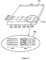
- FIG. 8 shows a reticle inspection system 900 where process 108 of Figure 1 of evaluating the reticle is implemented in one embodiment of the present invention.
- An autoloader 208 for automatically transporting reticles includes a robot 212 having an arm 210 extending towards a inspection port 202 of a reticle inspection station 250. Arm 210 may rotate and extend towards an external port 204 when in its state denoted by reference number 210'. Similarly, when in its state denoted by reference number 210", the robotic arm can also extend towards a storage port 206 of a reticle stocker station 216 that typically includes several slots or tracks for storing reticles. The robotic arm is designed to further extend and retrieve a reticle 214 from reticle stocker station 216.
- a typical inspection process may begin after reticle 214 is placed on external port 204, with the intention of storing the reticle in reticle stocker station 216 until it is used in a subsequent inspection application, for example.
- Robotic arm in its position 210' transports the reticle from external port 204 and stores it in a loading port of reticle stocker station 216 by extending as shown in Figure 8 .
- robotic arm 210" retrieves reticle 214 from the loading port and places it on inspection port 202 of reticle inspection station.
- the reticle inspection station 250 is coupled with a computer system 252 where evaluation process 108 of Figure 1 detailed above is carried out and it is determined whether the reticle has passed inspection.
- the computer system 252 may be integral to reticle inspection station 250 or separate from the inspection station 250.
- the reticle inspection station 250 receives design data 254 in the form of a list of figures, for example. Additionally, the computer system 252 receives image data (i.e., a test image) from the inspection station 250. The image data is analyzed by comparing it to a baseline image, which may be generated from the design data 254 or from the reticle 214. After the reticle inspection has concluded, reticle 214 is placed on external port 204 so that it may be carried to a fabrication facility for use, assuming of course, that it has passed inspection. Alternatively, the reticle 214 may be repaired or remade.
- Suitable computer systems for use in implementing and controlling the methods in the present invention may be obtained from various vendors (e.g. , Silicon Graphics of Mountain View, CA or Sun Mircosystems of Sunnyvale, CA) or custom built by a reticle inspection system vendor, such as KLA-Tencor.
- electronic representation covers any machine readable representation. Typically, such representations are stored on magnetic, electronic, or optically readable media. The content of such representations may be transmitted as electrical signals, magnetic signals, electromagnetic signals, optical signals, etc.
- an optical, electron beam, or other inspection system is integrated with a computer system which implements many of the method steps of this invention.
- Such composite system preferably includes at least (a) a baseline image (preferably compacted) stored in memory, (b) an imaging system arranged to generate an optical or electron beam image of the reticle, and (c) a processing unit configured to compare the baseline and current test images and thereby identify defects, as well as compute and store various statistical information.
- the imaging system will usually include (i) a source of illumination oriented to direct radiation onto a specified location of the reticle: and (ii) one or more detectors oriented to detect an image of the reticle from the source which has been scattered by the reticle.
- the imaging system may also include a scanning means.
- the collected statistical information may be utilized after the reticle is used to form patterns on a semiconductor wafer. That is, the statistical information may be used to correlate wafer statistical information, and hence separate the new errors introduced during wafer processing from the errors on the reticle. Accordingly, the present embodiments are to be considered as illustrative and not restrictive, and the invention is not to be limited to the details given herein, but may be modified within the scope of the appended claims.
Landscapes
- Engineering & Computer Science (AREA)
- Quality & Reliability (AREA)
- Computer Vision & Pattern Recognition (AREA)
- Physics & Mathematics (AREA)
- General Physics & Mathematics (AREA)
- Theoretical Computer Science (AREA)
- Exposure And Positioning Against Photoresist Photosensitive Materials (AREA)
- Investigating Materials By The Use Of Optical Means Adapted For Particular Applications (AREA)
- Image Processing (AREA)
- Image Analysis (AREA)
- Preparing Plates And Mask In Photomechanical Process (AREA)
Claims (43)
- Procédé d'examen d'un réticule définissant un motif de couche de circuit qui est utilisé dans un processus à semi-conducteur correspondant pour générer des motifs correspondants sur une tranche de semi-conducteur, le procédé comprenant :(a) la fourniture d'une image d'essai du réticule (604), l'image d'essai ayant une pluralité de valeurs caractéristiques d'essai ;(b) la fourniture d'une image de ligne de base contenant un motif attendu de l'image d'essai (601), l'image de ligne de base ayant une pluralité de valeurs caractéristiques de ligne de base qui correspondent aux valeurs caractéristiques d'essai ;(c) la comparaison des valeurs caractéristiques d'essai aux valeurs caractéristiques de ligne de base (308) de sorte qu'une pluralité de valeurs de différence soit calculée pour chaque paire de valeurs caractéristiques d'essai et de ligne de base ; et(d) la collecte d'informations statistiquescaractérisé en ce que :les informations statistiques sont collectées lorsque les valeurs caractéristiques d'essai sont comparées aux valeurs caractéristiques de ligne de base pour la pluralité de valeurs caractéristiques d'essai (310), dans lequel les informations statistiques comprennent une valeur moyenne ou médiane de la pluralité de valeurs caractéristiques d'essai ou des valeurs de différence.
- Procédé selon la revendication 1, dans lequel les informations statistiques sont collectées d'après une seconde pluralité de valeurs caractéristiques d'essai qui sont d'un type de caractéristique différent de la première pluralité de valeurs caractéristiques d'essai qui sont comparées aux valeurs caractéristiques de ligne de base.
- Procédé selon la revendication 2, dans lequel les premières valeurs caractéristiques d'essai sont sous forme de valeurs de position de bord et les secondes valeurs caractéristiques d'essai sont choisies dans le groupe constitué de valeurs de largeur de raies, de valeurs d'arrondissement d'angles, de valeurs de transmission, de valeurs de largeur de raies de grille, de valeurs de surface de contact, et de valeurs de désalignement.
- Procédé selon les revendications 2 ou 3, dans lequel les informations statistiques sont collectées d'après les secondes valeurs caractéristiques d'essai en fonction d'un paramètre prédéterminé.
- Procédé selon la revendication 4, dans lequel le paramètre prédéterminé est une position sur le réticule.
- Procédé selon la revendication 4, dans lequel le paramètre prédéterminé est une valeur de densité de particularité d'une surface sur le réticule.
- Procédé selon la revendication 4, dans lequel le paramètre prédéterminé est le processus correspondant du réticule, et l'écart type est déterminé pour une pluralité de réticules employés dans le processus.
- Procédé selon l'une quelconque des revendications 1, dans lequel les informations statistiques comprennent en outre une ou plusieurs des valeurs suivantes : une valeur maximale, une valeur minimale, ou une valeur de plage de la pluralité des valeurs caractéristiques d'essai de l'image d'essai.
- Procédé selon l'une quelconque des revendications 1 à 8, comprenant en outre le signalement d'une erreur pour une valeur choisie des valeurs caractéristiques d'essai si la valeur caractéristique d'essai choisie et la valeur caractéristique de ligne de base correspondante ont une valeur de différence associée qui est supérieure à un seuil prédéterminé.
- Procédé selon la revendication 8, dans lequel les valeurs moyenne, maximale, minimale, de plage, médiane et d'écart type sont corrélées à une région particulière du réticule.
- Procédé selon la revendication 10, dans lequel les valeurs moyenne, maximale, minimale, de plage, médiane et d'écart type sont en outre corrélées à une valeur de densité de particularité de la région particulière du réticule.
- Procédé selon la revendication 11, dans lequel les valeurs moyenne, maximale, minimale, de plage, médiane et d'écart type sont corrélées à un processus particulier associé au réticule.
- Procédé selon la revendication 1, dans lequel les informations statistiques sont collectées d'après la même pluralité de valeurs caractéristiques d'essai que la pluralité de valeurs caractéristiques d'essai qui sont comparées aux valeurs caractéristiques de ligne de base.
- Procédé selon la revendication 13, dans lequel les informations statistiques sont collectées d'après les valeurs caractéristiques d'essai en fonction d'un paramètre prédéterminé.
- Procédé selon la revendication 14, dans lequel le paramètre prédéterminé est une position sur le réticule.
- Procédé selon la revendication 14, dans lequel le paramètre prédéterminé est une valeur de densité de particularité d'une surface sur le réticule.
- Procédé selon la revendication 14, dans lequel le paramètre prédéterminé est le processus correspondant du réticule, et les informations statistiques sont collectées pour une pluralité de réticules employés dans le processus.
- Procédé selon la revendication 9, comprenant en outre l'ajustement du seuil prédéterminé pour des portions de l'image d'essai d'après les informations statistiques collectées.
- Procédé selon la revendication 1, dans lequel les valeurs caractéristiques d'essai qui sont utilisées dans la comparaison forment un premier sous-groupe et les valeurs caractéristiques d'essai sur lesquelles sont fondées les informations statistiques forment un second sous-groupe, le procédé comprenant en outre :l'ajustement d'un paramètre de processus d'un processus de réticule si les informations statistiques indiquent que le second sous-groupe de valeurs caractéristiques d'essai s'écarte des valeurs caractéristiques de ligne de base de plus d'une quantité prédéterminée.
- Procédé selon la revendication 19, dans lequel le premier sous-groupe est égal au second sous-groupe de valeurs caractéristiques d'essai.
- Procédé selon les revendications 19 ou 20, dans lequel les informations statistiques comprennent un paramètre choisi dans le groupe constitué d'une valeur d'écart type, d'une valeur minimale, d'une valeur maximale, d'une valeur de plage et d'une valeur médiane ou moyenne du second sous-groupe de valeurs caractéristiques d'essai.
- Procédé selon l'une quelconque des revendications 19 à 21, dans lequel le second sous-groupe de valeurs caractéristiques d'essai est choisi dans le groupe constitué de valeurs de largeur de raies, de valeurs d'arrondissement d'angles, de valeurs de transmission, de valeurs de largeur de raies de grille, de valeurs de surface de contact, et de valeurs d'alignement.
- Procédé selon l'une quelconque des revendications 19 à 21, dans lequel les informations statistiques sont fondées sur des valeurs de particularités mesurées sur le réticule ou des valeurs de différence entre des particularités du réticule et des particularités correspondantes d'une image de ligne de base.
- Procédé selon la revendication 23, dans lequel les informations statistiques sont collectées d'après les valeurs mesurées ou les valeurs de différence en fonction d'une position sur le premier réticule.
- Procédé selon la revendication 23, dans lequel les informations statistiques sont collectées d'après les valeurs mesurées ou les valeurs de différence en fonction d'une valeur de densité de particularité d'une surface sur le premier réticule.
- Procédé selon la revendication 23, dans lequel les informations statistiques sont collectées d'après les valeurs mesurées ou les valeurs de différence en fonction du processus de réticule.
- Procédé selon l'une quelconque des revendications 19 à 21 ou 23 à 26, dans lequel le second sous-groupe de valeurs caractéristiques d'essai est choisi dans le groupe constitué de valeurs de largeur de raies, de valeurs d'arrondissement d'angles, de valeurs de transmission, de valeurs de largeur de raies de grille, de valeurs de surface de contact, et de valeurs de désalignement.
- Procédé selon l'une quelconque des revendications 19 à 27, comprenant en outre :la répétition des opérations (a) à (d) pour un second réticule ;la comparaison des informations statistiques pour le second réticule aux informations statistiques pour le premier réticule ; etl'ajustement d'un paramètre de processus du processus de réticule si les informations statistiques pour le second réticule varient des informations statistiques pour le premier réticule de plus d'une seconde quantité prédéterminée.
- Procédé selon la revendication 28, dans lequel le paramètre de processus du processus de réticule est ajusté de façon à réduire des variations du second sous-groupe de valeurs caractéristiques d'essai en fonction de la position du réticule.
- Procédé selon l'une quelconque des revendications 19 à 27, comprenant en outre l'ajustement d'un paramètre de processus du processus de réticule si les informations statistiques indiquent que le second sous-groupe de valeurs caractéristiques d'essai s'écarte de plus d'une quantité prédéterminée.
- Procédé selon la revendication 30, dans lequel le paramètre de processus du processus de réticule est ajusté de façon à réduire des variations du second sous-groupe de valeurs caractéristiques d'essai en fonction de la densité de particularité.
- Procédé selon la revendication 1, le procédé comprenant en outre l'ajustement d'un paramètre de processus du processus de semi-conducteur d'après au moins en partie les informations statistiques collectées.
- Procédé selon la revendication 32, comprenant en outre l'examen d'une couche de circuit, résultant du processus de semi-conducteur, d'après au moins en partie les informations statistiques.
- Procédé selon les revendications 32 ou 33, dans lequel les informations statistiques comprennent un paramètre choisi dans le groupe consistant d'une valeur d'écart type, d'une valeur minimale, d'une valeur maximale, d'une valeur de plage et d'une valeur médiane ou moyenne des valeurs caractéristiques choisies.
- Procédé selon l'une quelconque des revendications 32 à 34, dans lequel les valeurs caractéristiques choisies sont choisies dans le groupe constitué de valeurs de largeur de raies, de valeurs d'arrondissement d'angles, de valeurs de transmission, de valeurs de largeur de raies de grille, de valeurs de surface de contact, et de valeurs d'alignement.
- Procédé selon l'une quelconque des revendications 32 à 35, dans lequel les informations statistiques sont fondées sur des valeurs de particularités mesurées sur le réticule ou des valeurs de différence entre des particularités du réticule et des particularités correspondantes d'une image de ligne de base.
- Procédé selon la revendication 36, dans lequel les valeurs mesurées et les valeurs de différence sont fonction d'une position sur le réticule.
- Procédé selon la revendication 36, dans lequel les valeurs mesurées et les valeurs de différence sont fonction d'une valeur de densité de particularité d'une surface sur le réticule.
- Procédé selon la revendication 36, dans lequel les valeurs mesurées et les valeurs de différence sont fonction du processus correspondant du réticule.
- Support lisible par ordinateur contenant des instructions de programme permettant d'examiner un réticule définissant un motif de couche de circuit qui est utilisé dans un processus à semi-conducteur correspondant pour générer des motifs correspondants sur une tranche de semi-conducteur, le support lisible par ordinateur stockant :(a) un code lisible par ordinateur permettant de fournir une image d'essai du réticule, l'image d'essai ayant une pluralité de valeurs caractéristiques d'essai ;(b) un code lisible par ordinateur permettant de fournir une image de ligne de base contenant un motif attendu de l'image d'essai, l'image de ligne de base ayant une pluralité de valeurs caractéristiques de ligne de base qui correspondent aux valeurs caractéristiques d'essai ;(c) un code lisible par ordinateur permettant de comparer les valeurs caractéristiques d'essai aux valeurs caractéristiques de ligne de base de sorte qu'une pluralité de valeurs de différence soit calculée pour chaque paire de valeurs caractéristiques d'essai et de ligne de base ; et(d) un code lisible par ordinateur permettant de collecter des informations statistiquescaractérisé en ce que :le code lisible par ordinateur permettant de collecter les informations statistiques est configuré pour collecter les informations statistiques lorsque les valeurs caractéristiques d'essai sont comparées aux valeurs caractéristiques de ligne de base pour une pluralité de valeurs caractéristiques de l'image d'essai, les informations statistiques comportant une valeur moyenne ou médiane d'une pluralité de valeurs caractéristiques de l'image d'essai ou des valeurs de différence.
- Support lisible par ordinateur selon la revendication 40, le support lisible par ordinateur comprenant en outre un code lisible par ordinateur permettant d'examiner une couche de circuit, résultant du processus à semi- conducteur, d'après au moins en partie les informations statistiques.
- Support lisible par ordinateur selon la revendication 40, le support lisible par ordinateur comprenant en outre un code informatique permettant d'ajuster un paramètre de processus du processus de réticule si les informations statistiques indiquent que les valeurs caractéristiques d'essai s'écartent des valeurs caractéristiques de ligne de base de plus d'une quantité prédéterminée.
- Support lisible par ordinateur selon la revendication 42, comprenant en outre :un code informatique permettant de répéter des instructions de programmation de codes informatiques (a) à (d) pour un second réticule ;un code informatique permettant de comparer les informations statistiques pour le second réticule aux informations statistiques pour le premier réticule ; etun code informatique permettant d'ajuster un paramètre de processus du processus de réticule si les informations statistiques pour le second réticule varient des informations statistiques pour le premier réticule de plus d'une seconde quantité prédéterminée
Applications Claiming Priority (3)
| Application Number | Priority Date | Filing Date | Title |
|---|---|---|---|
| US09/304,437 US6516085B1 (en) | 1999-05-03 | 1999-05-03 | Apparatus and methods for collecting global data during a reticle inspection |
| US304437 | 1999-05-03 | ||
| PCT/US2000/011768 WO2000066549A2 (fr) | 1999-05-03 | 2000-04-28 | Dispositifs et procedes de collecte de donnees globales durant une inspection de reticule |
Publications (2)
| Publication Number | Publication Date |
|---|---|
| EP1178961A2 EP1178961A2 (fr) | 2002-02-13 |
| EP1178961B1 true EP1178961B1 (fr) | 2016-07-06 |
Family
ID=23176510
Family Applications (1)
| Application Number | Title | Priority Date | Filing Date |
|---|---|---|---|
| EP00928680.8A Expired - Lifetime EP1178961B1 (fr) | 1999-05-03 | 2000-04-28 | Dispositifs et procedes de collecte de donnees globales durant une inspection de reticule |
Country Status (4)
| Country | Link |
|---|---|
| US (2) | US6516085B1 (fr) |
| EP (1) | EP1178961B1 (fr) |
| JP (1) | JP4588222B2 (fr) |
| WO (1) | WO2000066549A2 (fr) |
Families Citing this family (27)
| Publication number | Priority date | Publication date | Assignee | Title |
|---|---|---|---|---|
| US6516085B1 (en) * | 1999-05-03 | 2003-02-04 | Kla-Tencor | Apparatus and methods for collecting global data during a reticle inspection |
| JP2002132986A (ja) * | 2000-10-18 | 2002-05-10 | Canon Inc | 情報提供方法及び情報提供システム |
| US6617087B1 (en) * | 2001-06-27 | 2003-09-09 | Advanced Micro Devices, Inc. | Use of scatterometry to measure pattern accuracy |
| US6882745B2 (en) * | 2002-12-19 | 2005-04-19 | Freescale Semiconductor, Inc. | Method and apparatus for translating detected wafer defect coordinates to reticle coordinates using CAD data |
| US7271891B1 (en) * | 2003-08-29 | 2007-09-18 | Kla-Tencor Technologies Corporation | Apparatus and methods for providing selective defect sensitivity |
| US7450748B2 (en) * | 2003-12-02 | 2008-11-11 | International Business Machines Corporation | Mask inspection process accounting for mask writer proximity correction |
| US7297453B2 (en) * | 2005-04-13 | 2007-11-20 | Kla-Tencor Technologies Corporation | Systems and methods for mitigating variances on a patterned wafer using a prediction model |
| US7303842B2 (en) * | 2005-04-13 | 2007-12-04 | Kla-Tencor Technologies Corporation | Systems and methods for modifying a reticle's optical properties |
| US7300729B2 (en) * | 2005-04-13 | 2007-11-27 | Kla-Tencor Technologies Corporation | Method for monitoring a reticle |
| US7300725B2 (en) * | 2005-04-13 | 2007-11-27 | Kla-Tencor Technologies Corporation | Method for determining and correcting reticle variations |
| US7617477B2 (en) * | 2005-09-09 | 2009-11-10 | Brion Technologies, Inc. | Method for selecting and optimizing exposure tool using an individual mask error model |
| US8321422B1 (en) | 2009-04-23 | 2012-11-27 | Google Inc. | Fast covariance matrix generation |
| US8396325B1 (en) | 2009-04-27 | 2013-03-12 | Google Inc. | Image enhancement through discrete patch optimization |
| US8611695B1 (en) | 2009-04-27 | 2013-12-17 | Google Inc. | Large scale patch search |
| US8391634B1 (en) * | 2009-04-28 | 2013-03-05 | Google Inc. | Illumination estimation for images |
| US8385662B1 (en) | 2009-04-30 | 2013-02-26 | Google Inc. | Principal component analysis based seed generation for clustering analysis |
| US8735030B2 (en) | 2010-04-15 | 2014-05-27 | Carl Zeiss Smt Gmbh | Method and apparatus for modifying a substrate surface of a photolithographic mask |
| US8798393B2 (en) | 2010-12-01 | 2014-08-05 | Google Inc. | Removing illumination variation from images |
| FR2974414B1 (fr) * | 2011-04-22 | 2013-04-12 | Saint Gobain | Procede d'analyse de la qualite d'un vitrage |
| US9208552B2 (en) | 2011-04-26 | 2015-12-08 | Kla-Tencor Corporation | Method and system for hybrid reticle inspection |
| US10401305B2 (en) | 2012-02-15 | 2019-09-03 | Kla-Tencor Corporation | Time-varying intensity map generation for reticles |
| US8938119B1 (en) | 2012-05-01 | 2015-01-20 | Google Inc. | Facade illumination removal |
| US9448343B2 (en) | 2013-03-15 | 2016-09-20 | Kla-Tencor Corporation | Segmented mirror apparatus for imaging and method of using the same |
| US9518935B2 (en) * | 2013-07-29 | 2016-12-13 | Kla-Tencor Corporation | Monitoring changes in photomask defectivity |
| US9875534B2 (en) | 2015-09-04 | 2018-01-23 | Kla-Tencor Corporation | Techniques and systems for model-based critical dimension measurements |
| US10451563B2 (en) | 2017-02-21 | 2019-10-22 | Kla-Tencor Corporation | Inspection of photomasks by comparing two photomasks |
| US11416982B2 (en) * | 2019-10-01 | 2022-08-16 | KLA Corp. | Controlling a process for inspection of a specimen |
Family Cites Families (39)
| Publication number | Priority date | Publication date | Assignee | Title |
|---|---|---|---|---|
| GB2129547B (en) * | 1982-11-02 | 1986-05-21 | Cambridge Instr Ltd | Reticle inspection |
| US4717644A (en) | 1982-12-20 | 1988-01-05 | International Business Machines Corporation | Hybrid electron beam and optical lithography method |
| JPS59157505A (ja) * | 1983-02-28 | 1984-09-06 | Hitachi Ltd | パタ−ン検査装置 |
| JPS6057929A (ja) * | 1983-09-09 | 1985-04-03 | Hitachi Ltd | パターン欠陥検出装置 |
| US4805123B1 (en) * | 1986-07-14 | 1998-10-13 | Kla Instr Corp | Automatic photomask and reticle inspection method and apparatus including improved defect detector and alignment sub-systems |
| US5267175A (en) | 1986-09-12 | 1993-11-30 | Digital Equipment Corporation | Data base access mechanism for rules utilized by a synthesis procedure for logic circuit design |
| US5150308A (en) | 1986-09-12 | 1992-09-22 | Digital Equipment Corporation | Parameter and rule creation and modification mechanism for use by a procedure for synthesis of logic circuit designs |
| US5097422A (en) | 1986-10-10 | 1992-03-17 | Cascade Design Automation Corporation | Method and apparatus for designing integrated circuits |
| US4989255A (en) | 1988-03-25 | 1991-01-29 | Texas Instruments Incorporated | Expansion of compact database for pattern inspector or writer |
| JPH02170279A (ja) * | 1988-12-23 | 1990-07-02 | Hitachi Ltd | 被検査対象パターンの欠陥検出方法及びその装置 |
| US5287290A (en) | 1989-03-10 | 1994-02-15 | Fujitsu Limited | Method and apparatus for checking a mask pattern |
| US5113451A (en) | 1989-10-16 | 1992-05-12 | Vlsi Technology, Inc. | Method for labelling polygons |
| JPH03278057A (ja) * | 1990-02-14 | 1991-12-09 | Toshiba Corp | パターン検査装置 |
| US5230075A (en) | 1990-06-04 | 1993-07-20 | General Electric Company | Database shadowing system with data tags that select an operation of the save command |
| JP3329805B2 (ja) * | 1990-08-29 | 2002-09-30 | 株式会社日立製作所 | 自動外観検査装置及び外観検査方法 |
| IL125217A (en) | 1990-12-04 | 1999-10-28 | Orbot Instr Ltd | Apparatus and method for microscopic inspection of articles |
| US5563702A (en) * | 1991-08-22 | 1996-10-08 | Kla Instruments Corporation | Automated photomask inspection apparatus and method |
| US5416722A (en) | 1992-11-19 | 1995-05-16 | Vlsi Technology, Inc. | System and method for compacting integrated circuit layouts |
| US5483461A (en) | 1993-06-10 | 1996-01-09 | Arcsys, Inc. | Routing algorithm method for standard-cell and gate-array integrated circuit design |
| JP3069215B2 (ja) * | 1993-06-30 | 2000-07-24 | ホーヤ株式会社 | フォトマスクパターンの評価方法及びその装置並びにパターン転写方法 |
| JPH0765040A (ja) | 1993-08-24 | 1995-03-10 | Matsushita Electric Ind Co Ltd | 機能データインターフェース方法および機能データインターフェース装置 |
| JPH07147309A (ja) * | 1993-11-25 | 1995-06-06 | Nikon Corp | 欠陥検査装置 |
| US5625568A (en) | 1993-12-22 | 1997-04-29 | Vlsi Technology, Inc. | Method and apparatus for compacting integrated circuits with standard cell architectures |
| JPH07249748A (ja) | 1994-03-14 | 1995-09-26 | Fujitsu Ltd | マスタースライス型lsiの設計装置 |
| JPH08137093A (ja) * | 1994-09-16 | 1996-05-31 | Toshiba Corp | 欠陥検査装置 |
| US5814829A (en) * | 1995-07-11 | 1998-09-29 | Qc Optics, Inc. | Multistation surface inspection system |
| US6292582B1 (en) | 1996-05-31 | 2001-09-18 | Lin Youling | Method and system for identifying defects in a semiconductor |
| JP3660763B2 (ja) * | 1996-06-26 | 2005-06-15 | 株式会社日立製作所 | 被検査パターンの検査方法及び製造プロセス診断方法並びに半導体基板の製造方法 |
| JP4001653B2 (ja) * | 1996-08-29 | 2007-10-31 | ケーエルエー・インストルメンツ・コーポレーション | 試料からの多重チャネル応答を用いた試料の光学的検査 |
| US5804340A (en) | 1996-12-23 | 1998-09-08 | Lsi Logic Corporation | Photomask inspection method and inspection tape therefor |
| JPH10213422A (ja) * | 1997-01-29 | 1998-08-11 | Hitachi Ltd | パタ−ン検査装置 |
| JPH10242038A (ja) | 1997-02-28 | 1998-09-11 | Toshiba Corp | パターン形成方法とリソグラフィシステム |
| JP3484042B2 (ja) | 1997-05-21 | 2004-01-06 | 株式会社日立製作所 | パターン検査方法およびその装置 |
| US6009251A (en) | 1997-09-30 | 1999-12-28 | Synopsys, Inc. | Method and system for layout verification of an integrated circuit design with reusable subdesigns |
| US6097884A (en) | 1997-12-08 | 2000-08-01 | Lsi Logic Corporation | Probe points and markers for critical paths and integrated circuits |
| JP4002655B2 (ja) * | 1998-01-06 | 2007-11-07 | 株式会社日立製作所 | パターン検査方法およびその装置 |
| US6282309B1 (en) | 1998-05-29 | 2001-08-28 | Kla-Tencor Corporation | Enhanced sensitivity automated photomask inspection system |
| US6529621B1 (en) * | 1998-12-17 | 2003-03-04 | Kla-Tencor | Mechanisms for making and inspecting reticles |
| US6516085B1 (en) * | 1999-05-03 | 2003-02-04 | Kla-Tencor | Apparatus and methods for collecting global data during a reticle inspection |
-
1999
- 1999-05-03 US US09/304,437 patent/US6516085B1/en not_active Expired - Lifetime
-
2000
- 2000-04-28 WO PCT/US2000/011768 patent/WO2000066549A2/fr active Application Filing
- 2000-04-28 JP JP2000615380A patent/JP4588222B2/ja not_active Expired - Fee Related
- 2000-04-28 EP EP00928680.8A patent/EP1178961B1/fr not_active Expired - Lifetime
-
2002
- 2002-12-04 US US10/314,030 patent/US6654489B2/en not_active Expired - Lifetime
Also Published As
| Publication number | Publication date |
|---|---|
| WO2000066549A2 (fr) | 2000-11-09 |
| US6654489B2 (en) | 2003-11-25 |
| WO2000066549A3 (fr) | 2001-01-11 |
| JP4588222B2 (ja) | 2010-11-24 |
| US20030091224A1 (en) | 2003-05-15 |
| JP2002543463A (ja) | 2002-12-17 |
| EP1178961A2 (fr) | 2002-02-13 |
| US6516085B1 (en) | 2003-02-04 |
Similar Documents
| Publication | Publication Date | Title |
|---|---|---|
| EP1178961B1 (fr) | Dispositifs et procedes de collecte de donnees globales durant une inspection de reticule | |
| US6529621B1 (en) | Mechanisms for making and inspecting reticles | |
| US6691052B1 (en) | Apparatus and methods for generating an inspection reference pattern | |
| US6966047B1 (en) | Capturing designer intent in reticle inspection | |
| KR102513717B1 (ko) | 픽셀 레벨 이미지 정량화를 위한 딥 러닝 기반 결함 검출 및 분류 스킴의 사용 | |
| US7135344B2 (en) | Design-based monitoring | |
| CN105652589B (zh) | 使用设计者意图数据检查晶片和掩模版的方法和系统 | |
| US7440093B1 (en) | Apparatus and methods for providing selective defect sensitivity | |
| US8151220B2 (en) | Methods for simulating reticle layout data, inspecting reticle layout data, and generating a process for inspecting reticle layout data | |
| US7853920B2 (en) | Method for detecting, sampling, analyzing, and correcting marginal patterns in integrated circuit manufacturing | |
| KR101285967B1 (ko) | 검사 데이터와 조합하여 설계 데이터를 활용하는 방법 및시스템 | |
| US7027143B1 (en) | Methods and systems for inspecting reticles using aerial imaging at off-stepper wavelengths | |
| US6784446B1 (en) | Reticle defect printability verification by resist latent image comparison | |
| US6581193B1 (en) | Apparatus and methods for modeling process effects and imaging effects in scanning electron microscopy | |
| US7788629B2 (en) | Systems configured to perform a non-contact method for determining a property of a specimen | |
| US10074036B2 (en) | Critical dimension uniformity enhancement techniques and apparatus | |
| US7297453B2 (en) | Systems and methods for mitigating variances on a patterned wafer using a prediction model | |
| US20080167829A1 (en) | Methods and systems for using electrical information for a device being fabricated on a wafer to perform one or more defect-related functions | |
| WO2006113126A2 (fr) | Procede de surveillance d'un reticule | |
| WO2010005700A2 (fr) | Procédé de détection de caractéristiques d’aide de sous-résolution surdimensionnées | |
| JP2000347384A (ja) | 集束イオンビーム修正装置及び欠陥保証方法 | |
| KR20010003507A (ko) | 포토마스크 검사방법 |
Legal Events
| Date | Code | Title | Description |
|---|---|---|---|
| PUAI | Public reference made under article 153(3) epc to a published international application that has entered the european phase |
Free format text: ORIGINAL CODE: 0009012 |
|
| 17P | Request for examination filed |
Effective date: 20011115 |
|
| AK | Designated contracting states |
Kind code of ref document: A2 Designated state(s): AT BE CH CY DE DK ES FI FR GB GR IE IT LI LU MC NL PT SE |
|
| RIN1 | Information on inventor provided before grant (corrected) |
Inventor name: JUANG, SHAUH-TEH Inventor name: YE, JUN Inventor name: LU, YEN-WEN Inventor name: WILEY, JAMES, N. Inventor name: CAO, YU Inventor name: ALLES, DAVID, S. |
|
| RBV | Designated contracting states (corrected) |
Designated state(s): DE FR GB NL |
|
| 17Q | First examination report despatched |
Effective date: 20070118 |
|
| R17C | First examination report despatched (corrected) |
Effective date: 20070903 |
|
| REG | Reference to a national code |
Ref country code: DE Ref legal event code: R079 Ref document number: 60049377 Country of ref document: DE Free format text: PREVIOUS MAIN CLASS: C07C0405000000 Ipc: G06T0007000000 |
|
| RIC1 | Information provided on ipc code assigned before grant |
Ipc: G06T 7/00 20060101AFI20151222BHEP |
|
| GRAP | Despatch of communication of intention to grant a patent |
Free format text: ORIGINAL CODE: EPIDOSNIGR1 |
|
| INTG | Intention to grant announced |
Effective date: 20160205 |
|
| GRAS | Grant fee paid |
Free format text: ORIGINAL CODE: EPIDOSNIGR3 |
|
| GRAA | (expected) grant |
Free format text: ORIGINAL CODE: 0009210 |
|
| AK | Designated contracting states |
Kind code of ref document: B1 Designated state(s): DE FR GB NL |
|
| REG | Reference to a national code |
Ref country code: GB Ref legal event code: FG4D |
|
| REG | Reference to a national code |
Ref country code: DE Ref legal event code: R096 Ref document number: 60049377 Country of ref document: DE |
|
| REG | Reference to a national code |
Ref country code: NL Ref legal event code: FP |
|
| REG | Reference to a national code |
Ref country code: DE Ref legal event code: R097 Ref document number: 60049377 Country of ref document: DE |
|
| PLBE | No opposition filed within time limit |
Free format text: ORIGINAL CODE: 0009261 |
|
| STAA | Information on the status of an ep patent application or granted ep patent |
Free format text: STATUS: NO OPPOSITION FILED WITHIN TIME LIMIT |
|
| 26N | No opposition filed |
Effective date: 20170407 |
|
| GBPC | Gb: european patent ceased through non-payment of renewal fee |
Effective date: 20170428 |
|
| REG | Reference to a national code |
Ref country code: FR Ref legal event code: ST Effective date: 20171229 |
|
| PG25 | Lapsed in a contracting state [announced via postgrant information from national office to epo] |
Ref country code: FR Free format text: LAPSE BECAUSE OF NON-PAYMENT OF DUE FEES Effective date: 20170502 |
|
| PG25 | Lapsed in a contracting state [announced via postgrant information from national office to epo] |
Ref country code: GB Free format text: LAPSE BECAUSE OF NON-PAYMENT OF DUE FEES Effective date: 20170428 |
|
| PGFP | Annual fee paid to national office [announced via postgrant information from national office to epo] |
Ref country code: NL Payment date: 20180426 Year of fee payment: 19 |
|
| PGFP | Annual fee paid to national office [announced via postgrant information from national office to epo] |
Ref country code: DE Payment date: 20180427 Year of fee payment: 19 |
|
| REG | Reference to a national code |
Ref country code: DE Ref legal event code: R119 Ref document number: 60049377 Country of ref document: DE |
|
| REG | Reference to a national code |
Ref country code: NL Ref legal event code: MM Effective date: 20190501 |
|
| PG25 | Lapsed in a contracting state [announced via postgrant information from national office to epo] |
Ref country code: DE Free format text: LAPSE BECAUSE OF NON-PAYMENT OF DUE FEES Effective date: 20191101 Ref country code: NL Free format text: LAPSE BECAUSE OF NON-PAYMENT OF DUE FEES Effective date: 20190501 |
|
| P01 | Opt-out of the competence of the unified patent court (upc) registered |
Effective date: 20230525 |