EP1178705A1 - Composite substrate and el device comprising the same - Google Patents
Composite substrate and el device comprising the same Download PDFInfo
- Publication number
- EP1178705A1 EP1178705A1 EP01902771A EP01902771A EP1178705A1 EP 1178705 A1 EP1178705 A1 EP 1178705A1 EP 01902771 A EP01902771 A EP 01902771A EP 01902771 A EP01902771 A EP 01902771A EP 1178705 A1 EP1178705 A1 EP 1178705A1
- Authority
- EP
- European Patent Office
- Prior art keywords
- substrate
- composite substrate
- electrode
- dielectric layer
- oxide
- Prior art date
- Legal status (The legal status is an assumption and is not a legal conclusion. Google has not performed a legal analysis and makes no representation as to the accuracy of the status listed.)
- Withdrawn
Links
Images

Classifications
-
- H—ELECTRICITY
- H05—ELECTRIC TECHNIQUES NOT OTHERWISE PROVIDED FOR
- H05B—ELECTRIC HEATING; ELECTRIC LIGHT SOURCES NOT OTHERWISE PROVIDED FOR; CIRCUIT ARRANGEMENTS FOR ELECTRIC LIGHT SOURCES, IN GENERAL
- H05B33/00—Electroluminescent light sources
- H05B33/12—Light sources with substantially two-dimensional [2D] radiating surfaces
- H05B33/22—Light sources with substantially two-dimensional [2D] radiating surfaces characterised by the chemical or physical composition or the arrangement of auxiliary dielectric or reflective layers
-
- H—ELECTRICITY
- H05—ELECTRIC TECHNIQUES NOT OTHERWISE PROVIDED FOR
- H05B—ELECTRIC HEATING; ELECTRIC LIGHT SOURCES NOT OTHERWISE PROVIDED FOR; CIRCUIT ARRANGEMENTS FOR ELECTRIC LIGHT SOURCES, IN GENERAL
- H05B33/00—Electroluminescent light sources
- H05B33/02—Details
-
- H—ELECTRICITY
- H05—ELECTRIC TECHNIQUES NOT OTHERWISE PROVIDED FOR
- H05B—ELECTRIC HEATING; ELECTRIC LIGHT SOURCES NOT OTHERWISE PROVIDED FOR; CIRCUIT ARRANGEMENTS FOR ELECTRIC LIGHT SOURCES, IN GENERAL
- H05B33/00—Electroluminescent light sources
- H05B33/10—Apparatus or processes specially adapted to the manufacture of electroluminescent light sources
-
- H—ELECTRICITY
- H05—ELECTRIC TECHNIQUES NOT OTHERWISE PROVIDED FOR
- H05B—ELECTRIC HEATING; ELECTRIC LIGHT SOURCES NOT OTHERWISE PROVIDED FOR; CIRCUIT ARRANGEMENTS FOR ELECTRIC LIGHT SOURCES, IN GENERAL
- H05B33/00—Electroluminescent light sources
- H05B33/12—Light sources with substantially two-dimensional [2D] radiating surfaces
-
- Y—GENERAL TAGGING OF NEW TECHNOLOGICAL DEVELOPMENTS; GENERAL TAGGING OF CROSS-SECTIONAL TECHNOLOGIES SPANNING OVER SEVERAL SECTIONS OF THE IPC; TECHNICAL SUBJECTS COVERED BY FORMER USPC CROSS-REFERENCE ART COLLECTIONS [XRACs] AND DIGESTS
- Y10—TECHNICAL SUBJECTS COVERED BY FORMER USPC
- Y10S—TECHNICAL SUBJECTS COVERED BY FORMER USPC CROSS-REFERENCE ART COLLECTIONS [XRACs] AND DIGESTS
- Y10S428/00—Stock material or miscellaneous articles
- Y10S428/917—Electroluminescent
Definitions
- This invention relates to a composite substrate having a dielectric and an electrode, and an electroluminescent (EL) device using the same.
- electroluminescence The phenomenon that a material emits light upon application of an electric field is known as electroluminescence (EL). Devices utilizing this phenomenon are on commercial use as backlight in liquid crystal displays (LCD) and watches.
- LCD liquid crystal displays
- the EL devices include dispersion type devices of the structure that a dispersion of a powder phosphor in an organic material or enamel is sandwiched between electrodes, and thin-film type devices in which a thin-film phosphor sandwiched between two electrodes and two insulating thin films is formed on an electrically insulating substrate.
- the drive modes include DC voltage drive mode and AC voltage drive mode.
- the dispersion type EL devices are known from the past and have the advantage of easy manufacture, but their use is limited because of a low luminance and a short lifetime.
- the thin-film type EL devices have markedly spread the practical range of EL device application by virtue of a high luminance and a long lifetime.
- the predominant structure is such that blue sheet glass customarily used in liquid crystal displays and plasma display panels (PDP) is employed as the substrate, a transparent electrode of ITO or the like is used as the electrode in contact with the substrate, and the phosphor emits light which exits from the substrate side.
- PDP liquid crystal displays and plasma display panels
- a transparent electrode of ITO or the like is used as the electrode in contact with the substrate
- the phosphor emits light which exits from the substrate side.
- Mn-doped ZnS which emits yellowish orange light has been often used from the standpoints of ease of deposition and light emitting characteristics.
- the use of phosphor materials which emit light in the primaries of red, green and blue is essential to manufacture color displays.
- FIG. 2 illustrates the basic structure of this device.
- the EL device in FIG. 2 is structured such that a lower electrode 12, a thick-film dielectric layer 13, a light emitting layer 14, a thin-film insulating layer 15 and an upper electrode 16 are successively formed on a substrate 11 of ceramic or similar material. Since the light emitted by the phosphor exits from the upper side of the EL structure opposite to the substrate as opposed to the prior art structure, the upper electrode is a transparent electrode.
- the thick-film dielectric has a thickness of several tens of microns which is about several hundred to several thousand times the thickness of the thin-film insulator. This offers advantages including a minimized chance of breakdown caused by pinholes or the like, high reliability, and high manufacturing yields.
- Use of the thick dielectric invites a drop of the voltage applied to the phosphor layer, which is overcome by using a high-permittivity material as the dielectric layer.
- Use of the ceramic substrate and the thick-film dielectric permits a higher temperature for heat treatment. As a result, it becomes possible to deposit a light emitting material having good luminescent characteristics, which was impossible in the prior art because of the presence of crystal defects.
- Preferred conditions for the dielectric material used as the thick-film dielectric include high permittivity, insulation resistance, and dielectric strength.
- the substrate material is widespread crystallized glass or Al 2 O 3 and the dielectric material is BaTiO 3 which is widely used as capacitor material because of good dielectric characteristics, there arises a problem that cracks develop in the BaTiO 3 dielectric layer upon firing. Since the dielectric layer has a reduced dielectric strength due to such cracks, an EL device fabricated using this composite substrate is likely to break down. The cause is presumably the difference in coefficient of thermal expansion between the substrate material and the dielectric, which has a significant influence since the dielectric must be fired at high temperatures.
- lead-base dielectric materials having a relatively low firing temperature have been under predominant consideration as the dielectric material, as disclosed in JP-A 7-50197 and JP-B 7-44072.
- lead-base dielectric materials generally have a lower firing temperature than BaTiO 3 , which prevents the heat treating temperature of a phosphor layer from being elevated, so that EL devices using them fail to provide satisfactory luminescent characteristics.
- An object of the invention is to provide a composite substrate which suppresses reaction of a substrate with a dielectric layer that can otherwise cause degradation of the dielectric layer and which can be sintered at high temperature while minimizing the generation of cracks in the dielectric layer, as well as an EL device using the same.
- the specific substrate material and the dielectric material of the specific composition are used according to the invention, there is fabricated a composite substrate which can be sintered at a high temperature without incurring reaction of the dielectric layer with the substrate that can otherwise cause degradation of the dielectric layer and which has a thick-film dielectric layer free of cracks.
- the heat treating temperature of a phosphor layer can be increased whereby crystal defects in the phosphor layer are reduced and improved luminescent characteristics are obtainable.
- This function is effective especially when a Ce-doped SrS phosphor layer capable of emitting blue light is deposited.
- the dielectric layer has a high dielectric strength due to the absence of cracks, allowing high voltage drive ensuring improved luminescent characteristics.
- the composite substrate of the invention has the construction that an electrode and a dielectric layer are successively formed on an electrically insulating substrate.
- the substrate has a coefficient of thermal expansion of 10 to 20 ppm/K -1 and is preferably composed mainly of magnesia (MgO), steatite (MgO ⁇ SiO 2 ) or forsterite (2MgO ⁇ SiO 2 ).
- the dielectric layer is a sintered ceramic body composed mainly of barium titanate (BaTiO 3 ).
- the dielectric layer may further contain one or more oxides selected from among rare earth oxides, MnO, MgO, WO 3 , SiO 2 , CaO, ZrO 2 , Nb 2 O 5 and Co 2 O 3 .
- FIG. 1 is a cross-sectional view of an electroluminescent (EL) device using a composite substrate according to the invention.
- the composite substrate is a ceramic laminate structure having a substrate 1 of the above-described composition, a thick-film electrode (or first electrode) 2 formed thereon in a predetermined pattern, and a dielectric layer (or first dielectric layer) 3 of sintered high-permittivity ceramic body formed thereon by a thick-film technique.
- the EL device using the composite substrate has a basic structure as shown in FIG. 1, for example, including a thin-film light emitting layer (or phosphor layer) 4, a thin-film insulating layer (or second insulating layer) 5, and a transparent electrode (or second electrode) 6, which are formed on the dielectric layer of the composite substrate by such a technique as vacuum evaporation, sputtering or CVD.
- a single insulating structure with the thin-film insulating layer omitted is also acceptable.
- the composite substrate and the EL device using the same according to the invention are characterized by the use as the substrate material of magnesia (MgO), steatite (MgO ⁇ SiO 2 ) or forsterite (2MgO ⁇ SiO 2 ) which does not react with BaTiO 3 of the dielectric layer up to high temperature and has a substantially equal coefficient of thermal expansion to that of BaTiO 3 .
- MgO magnesia
- steatite MgO ⁇ SiO 2
- 2MgO ⁇ SiO 2 forsterite
- the substrate material used is composed mainly of magnesia (MgO), steatite (MgO ⁇ SiO 2 ) or forsterite (2MgO ⁇ SiO 2 ). Any of these materials may be used although a substrate material having a substantially equal coefficient of thermal expansion to that of the dielectric material is preferable. Among others, magnesia is preferred.
- the substrate formed of such material preferably has a coefficient of thermal expansion of 10 to 20 ppm/K -1 , and especially about 12 to 18 ppm/K -1 .
- the lower electrode layer serving as the first electrode is formed at least on the insulated substrate side or within the insulating layer.
- the electrode layer which is exposed to high temperature during formation of the insulating layer or during heat treatment together with the light emitting layer may be a commonly used metallic electrode composed mainly of palladium, rhodium, iridium, rhenium, ruthenium, platinum, silver, gold, tantalum, nickel, chromium or titanium.
- the upper electrode layer serving as the second electrode may be a transparent electrode which is transmissive to light in the predetermined emission wavelength region.
- a transparent electrode of ZnO or ITO generally contains In 2 O 3 and SnO in the stoichiometric composition although the O content may somewhat deviate therefrom.
- the mixing proportion of SnO 2 to In 2 O 3 is preferably 1 to 20% by weight, and more preferably 5 to 12% by weight.
- IZO the mixing proportion of ZnO to In 2 O 3 is about 12 to 32% by weight.
- the electrode layer may be a silicon-based one.
- the silicon electrode layer may be either polycrystalline silicon (p-Si) or amorphous silicon (a-Si), or even single crystal silicon if desired.
- the electrode layer is doped with an impurity for imparting electric conductivity.
- Any dopant may be used as the impurity as long as it can impart the desired conductivity.
- Use may be made of dopants commonly used in the silicon semiconductor art.
- Exemplary dopants are B, P, As, Sb, Al and the like. Of these, B, P, As, Sb and Al are especially preferred.
- the preferred dopant concentration is about 0.001 to 5 at%.
- any of conventional methods such as evaporation, sputtering, CVD, sol-gel and printing/firing methods may be used. Particularly when a structure in which a thick film having an electrode built therein is formed on a substrate is fabricated, the same method as used for the dielectric thick film is preferred.
- the electrode layer should preferably have a resistivity of up to 1 ⁇ cm, especially about 0.003 to 0.1 ⁇ cm in order to apply an effective electric field across the light emitting layer.
- the preferred thickness of the electrode layer is about 50 to 10,000 nm, more preferably about 100 to 5,000 nm, especially about 100 to 3,000 nm, though it depends on the identity of electrode material.
- the dielectric thick-film materials used as the first insulating layer include well-known dielectric thick-film materials. Those materials having a relatively high permittivity, dielectric strength and insulation resistance are preferred.
- such materials as lead titanate, lead niobate and barium titanate base materials may be used as the main component.
- Barium titanate (BaTiO 3 ) is especially preferred in relation to the substrate.
- the dielectric layer may further contain as an auxiliary component one or more oxides selected from among manganese oxide (MnO), magnesium oxide (MgO), tungsten oxide (WO 3 ), calcium oxide (CaO), zirconium oxide (ZrO 2 ), niobium oxide (Nb 2 O 5 ) and cobalt oxide (Co 2 O 3 ) or the oxide or oxides of one or more elements selected from among rare earth elements Sc, Y, La, Ce, Pr, Nd, Pm, Sm, Eu, Gd, Tb, Dy, Ho, Er, Tm, Yb and Lu.
- the auxiliary component is preferably contained in an amount of up to 50 mol%, more preferably 0.004 to 40 mol%, and even more preferably 0.01 to 30 mol% based on the main component, especially BaTiO 3 .
- the dielectric layer may further contain a vitreous component of silicon oxide (SiO 2 ), preferably in an amount of up to 2% by weight, especially 0.05 to 0.5% by weight.
- a vitreous component of silicon oxide (SiO 2 ) preferably in an amount of up to 2% by weight, especially 0.05 to 0.5% by weight. The inclusion of the vitreous component leads to an improvement in sinterability.
- any one or a mixture of two or more of the following materials may be used.
- ferroelectric Most of these materials are ferroelectric. These materials are described in further detail.
- BaTiO 3 and Sr family perovskite compounds are generally represented by the chemical formula ABO 3 wherein A and B each are a cation.
- A is at least one element selected from among Ca, Ba, Sr, Pb, K, Na, Li, La and Cd
- B is at least one element selected from among Ti, Zr, Ta and Nb.
- the ratio A/B in such perovskite type compounds is preferably between 0.8 and 1.3, and more preferably between 0.9 and 1.2.
- Ratios of A/B in the above range ensure the insulation of dielectrics and improve the crystallinity thereof, improving the dielectric or ferroelectric characteristics thereof. By contrast, at A/B ratios below 0.8, the crystallinity improving effect is not expectable. At A/B ratios beyond 1.3, it is difficult to form homogeneous thin films.
- the desired A/B is accomplished by controlling film depositing conditions.
- the proportion of O in ABO 3 is not limited to 3.
- Some perovskite materials form a stable perovskite structure when they are in short or excess of oxygen.
- ABO x the value of x is generally from about 2.7 to about 3.3. It is understood that the A/B ratio can be determined by x-ray fluorescence analysis.
- the ABO 3 type perovskite compound used herein may be any of A 1+ B 5+ O 3 , A 2+ B 4+ O 3 , A 3+ B 3+ O 3 , A x BO 3 , A(B' 0.67 B" 0.33 )O 3 , A(B' 0.33 B" 0.67 )O 3 , A(B 0.5 +3 B 0.5 +5 )O 3 , A(B 0.5 2+ B 0.5 6+ )O 3 , A(B 0.5 1+ B 0.5 7+ )O 3 , A 3+ (B 0.5 2+ B 0.5 4+ )O 3 , A(B 0.25 1+ B 0.75 5+ )O 3 , A(B 0.5 3+ B 0.5 4+ )O 2.75 , and A(B 0.5 2+ B 0.5 5+ )O 2.75 .
- More illustrative are lead family perovskite compounds such as PZT and PLZT, NaNbO 3 , KNbO 3 , NaTaO 3 , KTaO 3 , CaTiO 3 , SrTiO 3 , BaTiO 3 , BaZrO 3 , CaZrO 3 , SrZrO 3 , CdHfO 3 , CdZrO 3 , SrSnO 3 , LaAlO 3 , BiFeO 3 , bismuth family perovskite compounds, and solid solutions thereof.
- lead family perovskite compounds such as PZT and PLZT, NaNbO 3 , KNbO 3 , NaTaO 3 , KTaO 3 , CaTiO 3 , SrTiO 3 , BaTiO 3 , BaZrO 3 , CaZrO 3 , SrZrO 3 , CdHfO 3 , C
- PZT is a solid solution of PbZrO 3 -PbTiO 3 system.
- PLZT is a compound of PZT doped with La and has the formula: (Pb 0.89-0.91 La 0.11-0.09 )(Zr 0.65 Ti 0.35 )O 3 when represented according to the ABO 3 .
- bismuth family layer compounds are generally represented by the formula: Bi 2 A m-1 B m O 3m+3 wherein m is an integer of 1 to 5, A is selected from among Bi, Ca, Sr, Ba, Pb, Na, K and rare earth elements (inclusive of Sc and Y), and B is Ti, Ta or Nb.
- A is selected from among Bi, Ca, Sr, Ba, Pb, Na, K and rare earth elements (inclusive of Sc and Y)
- B is Ti, Ta or Nb.
- Illustrative are Bi 4 Ti 3 O 12 , SrBi 2 Ta 2 O 9 , and SrBi 2 Nb 2 O 9 . Any of these compounds or a solid solution thereof may be used in the practice of the invention.
- the preferred perovskite type compounds used herein are those having a high permittivity, for example, NaNbO 3 , KNbO 3 , KTaO 3 , CdHfO 3 , CdZrO 3 , BiFeO 3 and bismuth family perovskite compounds, with CdHfO 3 being more preferred.
- the tungsten bronze type materials are preferably those tungsten bronze type materials described in the collection of ferroelectric materials by Landoit-Borenstein, Vol. 16.
- the tungsten bronze type materials generally have the chemical formula: A y B 5 O 15 wherein A and B each are a cation.
- A is one or more elements of Mg, Ca, Ba, Sr, Pb, K, Na, Li, Rb, Tl, Bi, rare earth elements and Cd
- B is one or more elements selected from Ti, Zr, Ta, Nb, Mo, W, Fe and Ni.
- the ratio O/B in these tungsten bronze type materials is not limited to 15/5. Some tungsten bronze type materials form a stable tungsten bronze structure when they are in short or excess of oxygen.
- the ratio O/B is generally between about 2.6 and about 3.4.
- Illustrative examples include tungsten bronze type oxides, such as (Ba,Pb)Nb 2 O 6 , PbNb 2 O 6 , PbTa 2 O 6 , PbNb 4 O 11 , PbNb 2 O 6 , SBN (strontium barium niobate), Ba 2 KNb 5 O 15 , Ba 2 LiNb 5 O 15 , Ba 2 AgNb 5 O 15 , Ba 2 RbNb 5 O 15 , SrNb 2 O 6 , BaNb 2 O 6 , Sr 2 NaNb 5 O 15 , Sr 2 LiNb 5 O 15 , Sr 2 KNb 5 O 15 , Sr 2 RbNb 5 O 15 , Ba 3 Nb 10 O 28 , Bi 3 Nd 17 O 47 , K 3 Li 2 Nb 5 O 15 , K 2 RNb 5 O 15 (wherein R is Y, La, Ce, Pr, Nd, Sm, Eu, Gd, Tb, Dy or Ho),
- Sr 2 TlNb 5 O 15 Ba 2 NaNb 5 O 15 , and Ba 2 KNb 5 O 15 , and solid solutions thereof.
- Preferred among others are SBN ((Ba,Sr)Nb 2 O 6 ), Ba 2 KNb 5 O 15 , Ba 2 LiNb 5 O 15 , Ba 2 AgNb 5 O 15 , Sr 2 NaNb 5 O 15 , Sr 2 LiNb 5 O 15 , and Sr 2 KNb 5 O 15 .
- the YMnO 3 type materials have the chemical formula: RMnO 3 wherein R is preferably at least one rare earth element (inclusive of Sc and Y).
- the ratio R/Mn in the YMnO 3 type materials is preferably between 0.8 and 1.2, and more preferably between 0.9 and 1.1. Ratios of R/Mn in this range ensure the insulation of dielectrics and improve the crystallinity thereof, improving the ferroelectric characteristics thereof. By contrast, R/Mn ratios below 0.8 or above 1.2 tend to lower crystallinity. Especially at R/Mn ratios beyond 1.2, materials are likely to be paraelectric rather than ferroelectric and sometimes cannot be applied to devices utilizing polarization.
- the desired R/Mn is accomplished by controlling film depositing conditions. It is understood that the R/Mn ratio can be determined by x-ray fluorescence analysis.
- the preferred YMnO 3 type materials used herein have a hexagonal crystal structure.
- the existing YMnO 3 type materials include those having a hexagonal crystal structure and those having a rhombic crystal structure. To achieve the phase transition effect, hexagonal crystal materials are preferred.
- Illustrative are materials having a substantial composition of YMnO 3 , HoMnO 3 , ErMnO 3 , YbMnO 3 , TmMnO 3 or LuMnO 3 , or solid solutions thereof.
- the dielectric layer thick-film preferably has a resistivity of at least about 10 8 ⁇ cm, especially about 10 10 to 10 18 ⁇ cm.
- a material having a relatively high permittivity as well is preferred.
- the permittivity ⁇ is preferably about 100 to 10,000.
- the film thickness is preferably 5 to 50 ⁇ m, and more preferably 10 to 30 ⁇ m.
- any desired method may be used in forming the dielectric layer thick-film.
- a method capable of easily forming a film of 10 to 50 ⁇ m thick is recommended, with the sol-gel and printing/firing methods being preferred.
- a material having a properly selected particle size is mixed with a binder to form a paste having an appropriate viscosity.
- the paste is applied onto a substrate by a screen printing technique and dried.
- the green sheet is fired at a suitable temperature, yielding a thick film.
- the thick film thus obtained has asperities or holes as large as 1 ⁇ m or more, it is preferred in some embodiments to improve the surface flatness or smoothness by polishing the film or forming a smoothing layer thereon.
- the materials used in its light emitting layer includes ZnS and Mn/CdSSe as the red light emitting material, ZnS:TbOF and ZnS:Tb as the green light emitting material, and SrS:Ce, (SrS:Ce/ZnS)n, CaGa 2 S 4 :Ce, and SrGa 2 S 4 :Ce as the blue light emitting material.
- Multilayer films of SrS:Ce/ZnS:Mn and the like are known as the material capable of emitting white light.
- compositional ratio of these compounds does not strictly take the above-described value, but has a certain solid solution limit with respect to each element. Therefore, a compositional ratio within that range is acceptable.
- the EL phosphor thin-film is formed of a matrix material to which a luminescence center is added.
- a luminescence center selected from well-known transition metals and rare earth elements may be added in a conventional quantity.
- a rare earth element such as Ce or Eu or Cr, Fe, Co, Ni, Cu, Bi, Ag or the like in metallic or sulfide form is added to a raw material. Since the addition quantity varies with the raw material and the thin film to be formed, the composition of the raw material is adjusted so that the thin film may have an ordinary addition quantity.
- any of well-known techniques such as evaporation, sputtering, CVD, sol-gel and printing/firing techniques may be used in forming an EL phosphor thin-film from these materials.
- the thickness of the light emitting layer is not critical. Too large a thickness causes to increase the drive voltage whereas too small a thickness leads to a decline of emission efficiency.
- the thickness is preferably about 100 to 1,000 nm, and especially about 150 to 700 nm, though it depends on the identity of phosphor material.
- a sulfide phosphor of the desired composition is preferably formed at a high temperature in excess of 600°C or annealed at a high temperature in excess of 600°C, if desired.
- a high-temperature process is effective.
- the dielectric thick-film for inorganic EL devices according to the invention can withstand such high-temperature process.
- the inorganic EL device preferably includes a thin-film insulating layer (or second insulating layer) between the electrode layer and the phosphor thin-film (or light emitting layer).
- the materials of which the thin-film insulating layer is made include silicon oxide (SiO 2 ), silicon nitride (Si 3 N 4 ), tantalum oxide (Ta 2 O 5 ), strontium titanate (SrTiO 3 ), yttrium oxide (Y 2 O 3 ), barium titanate (BaTiO 3 ), lead titanate (PbTiO 3 ), PZT, zirconia (ZrO 2 ), silicon oxynitride (SiON), alumina (Al 2 O 3 ), lead niobate, PMN-PT base materials and multilayer or mixed thin-films thereof.
- the insulating layer thus formed preferably has a thickness of about 50 to 1,000 nm, and especially about 100 to 500 nm.
- another thin-film insulating layer may be formed in a duplex configuration using another material, if desired.
- an electrode layer (or second electrode) is preferably formed on the thin-film insulating layer.
- the material of the electrode layer is preferably selected from the electrode materials described above.
- an EL device can be constructed in this way. Since the phosphor thin-film can be formed by the high-temperature process, the performance of a blue phosphor which is short of luminance in the prior art can be significantly improved, and hence, a full-color EL display can be implemented. Further, since an insulating thick-film having a high density and free of cracks can be formed according to the invention, the EL device is less prone to breakdown and outstandingly increased in stability as compared with conventional thin-film dual insulating structure, achieving a higher luminance and a lower voltage.
- the composite substrate is preferably prepared by a conventional thick-film laminating technique. Specifically, onto a substrate of magnesia (MgO), steatite (MgO ⁇ SiO 2 ) or forsterite (2MgO ⁇ SiO 2 ), a paste using a conductive powder such as Pd or Pt as a source is printed in a pattern by a screen printing technique or the like. Further, a thick film is formed thereon using a dielectric paste prepared employing a powdery dielectric material as a source. Alternatively, the dielectric paste is cast to form a green sheet, which is placed and press bonded onto the electrode. It is also possible to print an electrode on a green sheet of dielectric, which is press bonded to a stress relief layer on the substrate.
- MgO magnesia
- steatite MgO ⁇ SiO 2
- 2MgO ⁇ SiO 2 forsterite
- a green laminate sheet consisting of a stress relief layer, electrode and dielectric is separately formed and press bonded to the substrate.
- the stress relief layer having a graded composition can be formed by successively stacking layers of varying composition.
- the structure thus constructed is fired at a temperature of 1,000°C to less than 1,600°C, preferably 1,200°C to 1,500°C, and more preferably 1,300°C to 1,450°C.
- a paste based on Pd powder was printed in a stripe pattern having a width of 1.6 mm and a gap of 1.5 mm as an electrode and dried for several minutes at 1,100°C.
- MnO, MgO, Y 2 O 3 , V 2 O 5 or (Ba, Ca)SiO 3 was added to BaTiO 3 powder in a predetermined concentration and mixed in water.
- the mixed powder was dried and admixed with a binder to form a dielectric paste.
- the dielectric paste thus obtained was printed onto the electrode pattern-printed substrate to a thickness of 30 ⁇ m, dried, and fired in air at 1,200°C for 2 hours.
- the dielectric layer as fired was 10 ⁇ m thick.
- a sample was separately prepared by printing a stripe pattern of Pd electrode having a width of 1.5 mm and a gap of 1.5 mm so as to extend perpendicular to the underlying electrode pattern after drying of the dielectric paste, drying and firing in the above-mentioned temperature profile.
- An EL device was constructed by sputtering a Mn-doped ZnS target, with the composite substrate heated at 250°C, to form a ZnS phosphor thin film of 0.7 ⁇ m thick, followed by heat treatment in vacuum for 10 minutes. Then a Si 3 N 4 thin film as the second insulating layer and an ITO thin film as the second electrode were successively formed by sputtering, completing the EL device.
- the luminescent characteristics of the EL device were determined by extending electrodes from the printed/fired electrode and the ITO transparent electrode of the cell structure obtained above and applying an electric field at a frequency of 1 kHz and a pulse width of 50 ⁇ s.
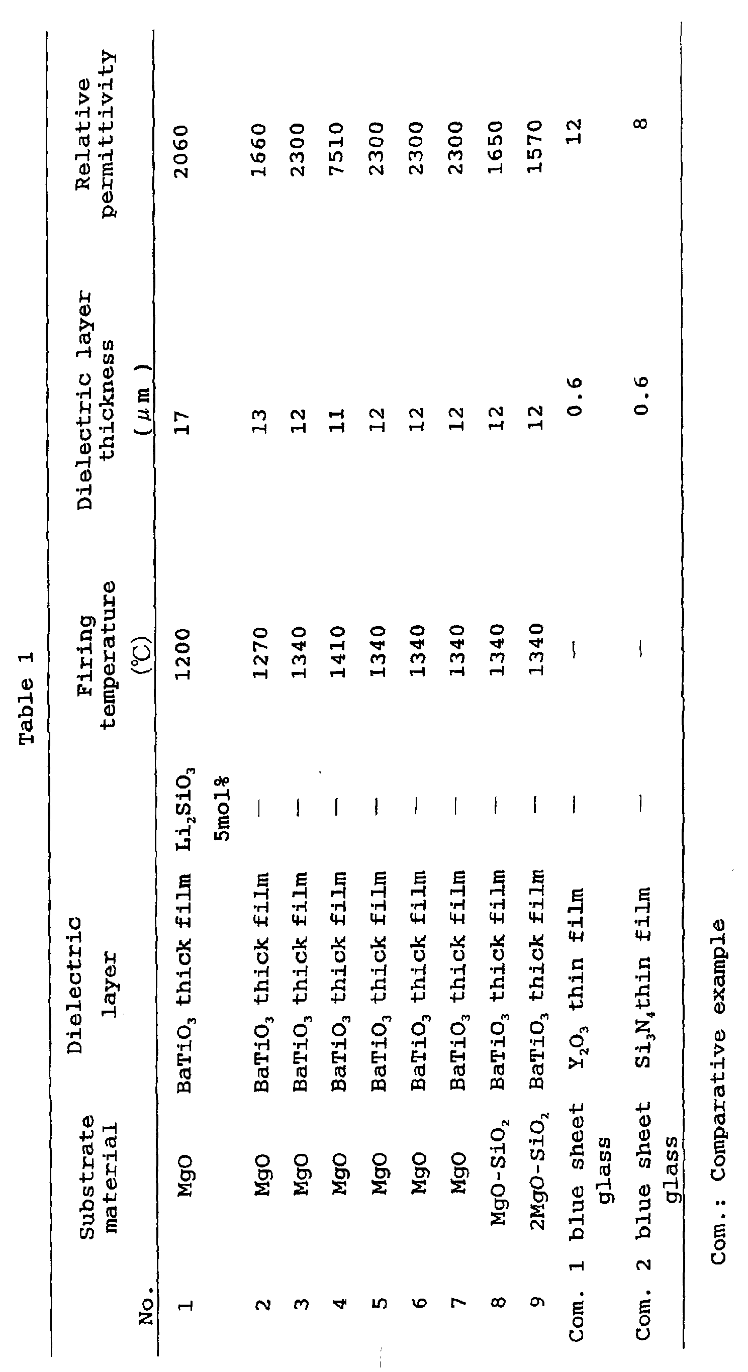
- Table 1 shows the electrical characteristics of the dielectric layers of the composite substrates prepared as above and the luminescent characteristics of the EL devices fabricated using the composite substrates.
- the inventive samples in which the coefficient of thermal expansion of substrates is adjusted optimum to permit use of a thick film of high permittivity material have a low emission start voltage as compared with prior art devices, and provide a higher emission luminance when the same voltage is applied. Elevating the heat treating temperature is effective for further reducing the emission start voltage.
- a composite substrate which suppresses reaction of a substrate with a dielectric layer that can otherwise cause degradation of the dielectric layer and which can be sintered at high temperature while minimizing the occurrence of cracks in the dielectric layer, and an EL device using the composite substrate.
Landscapes
- Engineering & Computer Science (AREA)
- Manufacturing & Machinery (AREA)
- Electroluminescent Light Sources (AREA)
- Laminated Bodies (AREA)
Abstract
Description
said substrate having a coefficient of thermal expansion of 10 to 20 ppm/K.
Illustrative are Bi4Ti3O12, SrBi2Ta2O9, and SrBi2Nb2O9. Any of these compounds or a solid solution thereof may be used in the practice of the invention.

Claims (8)
- A composite substrate in which an electrode and a dielectric layer are successively formed on an electrically insulating substrate,
said substrate having a coefficient of thermal expansion of 10 to 20 ppm/K. - The composite substrate of claim 1 wherein said substrate is composed mainly of magnesia (MgO), steatite (MgO·SiO2) or forsterite (2MgO·SiO2).
- The composite substrate of claim 1 or 2 wherein said substrate is a sintered ceramic body composed mainly of barium titanate (BaTiO3).
- The composite substrate of claim 3 wherein said dielectric layer contains one or more oxides selected from the group consisting of manganese oxide (MnO), magnesium oxide (MgO), tungsten oxide (WO3), calcium oxide (CaO), zirconium oxide (ZrO2), niobium oxide (Nb2O5) and cobalt oxide (Co2O3).
- The composite substrate of claim 3 or 4 wherein said dielectric layer contains the oxides of one or more elements selected from the group consisting of rare earth elements Sc, Y, La, Ce, Pr, Nd, Pm, Sm, Eu, Gd, Tb, Dy, Ho, Er, Tm, Yb and Lu.
- The composite substrate of any one of claims 3 to 5 wherein said dielectric layer contains a vitreous component composed of silicon oxide (SiO2).
- An EL device comprising at least a light emitting layer and a second electrode on the composite substrate of any one of claims 1 to 6.
- The EL device of claim 7 further comprising a second insulator layer between the light emitting layer and the second electrode.
Applications Claiming Priority (7)
| Application Number | Priority Date | Filing Date | Title |
|---|---|---|---|
| JP2000029465 | 2000-02-07 | ||
| JP2000029465A JP2001220217A (en) | 2000-02-07 | 2000-02-07 | Composite board el element using the same |
| JP2000059522 | 2000-03-03 | ||
| JP2000059521 | 2000-03-03 | ||
| JP2000059522A JP2001250677A (en) | 2000-03-03 | 2000-03-03 | Manufacturing method of complex substrate, complex substrate, and thin film light emission element using the same |
| JP2000059521A JP2001250683A (en) | 2000-03-03 | 2000-03-03 | Complex substrate, thin film light emission element using it, and its manufacturing method |
| PCT/JP2001/000813 WO2001060124A1 (en) | 2000-02-07 | 2001-02-06 | Composite substrate and el device comprising the same |
Publications (2)
| Publication Number | Publication Date |
|---|---|
| EP1178705A1 true EP1178705A1 (en) | 2002-02-06 |
| EP1178705A4 EP1178705A4 (en) | 2009-05-06 |
Family
ID=27342273
Family Applications (3)
| Application Number | Title | Priority Date | Filing Date |
|---|---|---|---|
| EP01902771A Withdrawn EP1178705A4 (en) | 2000-02-07 | 2001-02-06 | COMPOSITE SUBSTRATE AND EL DEVICE INCLUDING THE SAME |
| EP01902772A Withdrawn EP1173047A4 (en) | 2000-02-07 | 2001-02-06 | COMPOSITE SUBSTRATE, THIN-FILM ELECTROLUMINESCENT DEVICE COMPRISING THE SAME, AND PROCESS FOR PRODUCING THE SAME |
| EP01902773A Withdrawn EP1178707A1 (en) | 2000-02-07 | 2001-02-06 | Method for producing composite substrate, composite substrate, and el device comprising the same |
Family Applications After (2)
| Application Number | Title | Priority Date | Filing Date |
|---|---|---|---|
| EP01902772A Withdrawn EP1173047A4 (en) | 2000-02-07 | 2001-02-06 | COMPOSITE SUBSTRATE, THIN-FILM ELECTROLUMINESCENT DEVICE COMPRISING THE SAME, AND PROCESS FOR PRODUCING THE SAME |
| EP01902773A Withdrawn EP1178707A1 (en) | 2000-02-07 | 2001-02-06 | Method for producing composite substrate, composite substrate, and el device comprising the same |
Country Status (7)
| Country | Link |
|---|---|
| US (3) | US6709695B2 (en) |
| EP (3) | EP1178705A4 (en) |
| KR (3) | KR100443276B1 (en) |
| CN (3) | CN1198482C (en) |
| CA (3) | CA2366572C (en) |
| TW (1) | TW524028B (en) |
| WO (3) | WO2001060126A1 (en) |
Cited By (1)
| Publication number | Priority date | Publication date | Assignee | Title |
|---|---|---|---|---|
| EP4701334A1 (en) * | 2024-08-22 | 2026-02-25 | Datec Coating Technologies Ltd. | Self-limiting thick film positive temperature coefficient of resistivity (ptcr) resistor compositions |
Families Citing this family (39)
| Publication number | Priority date | Publication date | Assignee | Title |
|---|---|---|---|---|
| US7223483B2 (en) * | 2001-06-25 | 2007-05-29 | Showa Denko K.K. | Light-emitting material and organic light-emitting device |
| JP4748435B2 (en) * | 2001-08-21 | 2011-08-17 | 日本電気硝子株式会社 | Laminated glass ceramic material and laminated glass ceramic sintered body |
| KR100497213B1 (en) | 2001-10-29 | 2005-06-28 | 더 웨스타임 코퍼레이션 | Composite Substrate, EL Panel Comprising the Same, and Method for Producing the Same |
| ATE428291T1 (en) * | 2001-12-21 | 2009-04-15 | Ifire Ip Corp | LOW BURNING TEMPERATURE DIELECTRIC THICK FILM FOR ELECTROLUMINESCENT DEVICES |
| US6730615B2 (en) * | 2002-02-19 | 2004-05-04 | Intel Corporation | High reflector tunable stress coating, such as for a MEMS mirror |
| KR100506149B1 (en) * | 2002-07-22 | 2005-08-08 | 이충훈 | Manufacturing method of organic light emitting diode |
| EP1537763B1 (en) * | 2002-09-12 | 2007-03-21 | iFire Technology Corp. | Silicon oxynitride passivated rare earth activated thioaluminate phosphors for electroluminescent displays |
| JP3829935B2 (en) * | 2002-12-27 | 2006-10-04 | 信越化学工業株式会社 | High voltage resistance member |
| KR20040068772A (en) * | 2003-01-27 | 2004-08-02 | 엘지전자 주식회사 | Dielectric layer of plasma display panel and method of fabricating the same |
| JP2004265740A (en) * | 2003-02-28 | 2004-09-24 | Tdk Corp | El functional film and el element |
| US7659475B2 (en) * | 2003-06-20 | 2010-02-09 | Imec | Method for backside surface passivation of solar cells and solar cells with such passivation |
| JP4131218B2 (en) * | 2003-09-17 | 2008-08-13 | セイコーエプソン株式会社 | Display panel and display device |
| EP1669964A4 (en) * | 2003-09-30 | 2007-09-26 | Asahi Glass Co Ltd | MULTILAYER BODIES FOR FORMING A WIRING BASE, WIRING BASE, AND PROCESS FOR PRODUCING THE SAME |
| JP4085051B2 (en) * | 2003-12-26 | 2008-04-30 | 株式会社東芝 | Semiconductor device and manufacturing method thereof |
| WO2005075378A1 (en) * | 2004-02-06 | 2005-08-18 | Murata Manufacturing Co.,Ltd. | Ferroelectric ceramic composition and ferroelectricity application device utilizing the same |
| JP3951055B2 (en) * | 2004-02-18 | 2007-08-01 | セイコーエプソン株式会社 | Organic electroluminescence device and electronic device |
| JP4030515B2 (en) * | 2004-03-30 | 2008-01-09 | 本田技研工業株式会社 | Exhaust gas purification catalyst |
| US7741773B2 (en) * | 2004-04-09 | 2010-06-22 | Ifire Ip Corporation | Thick film dielectric structure for thick dielectric electroluminescent displays |
| US7815854B2 (en) * | 2004-04-30 | 2010-10-19 | Kimberly-Clark Worldwide, Inc. | Electroluminescent illumination source for optical detection systems |
| US20060019265A1 (en) * | 2004-04-30 | 2006-01-26 | Kimberly-Clark Worldwide, Inc. | Transmission-based luminescent detection systems |
| US7796266B2 (en) * | 2004-04-30 | 2010-09-14 | Kimberly-Clark Worldwide, Inc. | Optical detection system using electromagnetic radiation to detect presence or quantity of analyte |
| US20050253510A1 (en) * | 2004-05-11 | 2005-11-17 | Shogo Nasu | Light-emitting device and display device |
| JP2006164708A (en) | 2004-12-06 | 2006-06-22 | Semiconductor Energy Lab Co Ltd | Electronic equipment and light emitting device |
| US20070121113A1 (en) * | 2004-12-22 | 2007-05-31 | Cohen David S | Transmission-based optical detection systems |
| JP5355076B2 (en) * | 2005-04-15 | 2013-11-27 | アイファイアー・アイピー・コーポレーション | Magnesium oxide-containing barrier layer for dielectric thick film electroluminescent displays |
| KR100691437B1 (en) * | 2005-11-02 | 2007-03-09 | 삼성전기주식회사 | Polymer-ceramic dielectric compositions, embedded capacitors and printed circuit boards using the same |
| US20080131673A1 (en) * | 2005-12-13 | 2008-06-05 | Yasuyuki Yamamoto | Method for Producing Metallized Ceramic Substrate |
| KR100785022B1 (en) * | 2006-07-05 | 2007-12-11 | 삼성전자주식회사 | Electroluminescent element |
| WO2008075615A1 (en) * | 2006-12-21 | 2008-06-26 | Semiconductor Energy Laboratory Co., Ltd. | Light-emitting element and light-emitting device |
| JP2009069288A (en) * | 2007-09-11 | 2009-04-02 | Seiko Epson Corp | screen |
| KR20090041639A (en) * | 2007-10-24 | 2009-04-29 | 삼성전자주식회사 | Manufacturing method of distributed inorganic electroluminescent device and distributed inorganic electroluminescent device |
| US20090252933A1 (en) * | 2008-04-04 | 2009-10-08 | 3M Innovative Properties Company | Method for digitally printing electroluminescent lamps |
| NL1036735A1 (en) * | 2008-04-10 | 2009-10-13 | Asml Holding Nv | Shear-layer chuck for lithographic apparatus. |
| JP5762715B2 (en) * | 2010-10-06 | 2015-08-12 | 信越化学工業株式会社 | Magneto-optic material, Faraday rotator, and optical isolator |
| US8908349B2 (en) * | 2011-03-31 | 2014-12-09 | Ngk Insulators, Ltd. | Member for semiconductor manufacturing apparatus |
| JP2015199916A (en) * | 2014-04-02 | 2015-11-12 | Jsr株式会社 | Film forming composition and pattern forming method |
| CN105244450A (en) * | 2015-10-09 | 2016-01-13 | 北京大学深圳研究生院 | Organic light-emitting device driven by alternating electric field and preparation method for organic light-emitting device |
| US10186379B2 (en) * | 2016-06-28 | 2019-01-22 | Tdk Corporation | Dielectric composition and electronic component |
| DE102018117210A1 (en) * | 2018-07-17 | 2020-02-20 | Helmholtz-Zentrum Dresden - Rossendorf E.V. | Layer sequence for the generation of electroluminescence and its use |
Family Cites Families (32)
| Publication number | Priority date | Publication date | Assignee | Title |
|---|---|---|---|---|
| JPS6084692A (en) * | 1983-08-08 | 1985-05-14 | ライフ・ライト・システムズ | Emergency signal apparatus |
| JPH0744072B2 (en) | 1985-04-05 | 1995-05-15 | 日本電気株式会社 | EL device and manufacturing method thereof |
| JPS61230294A (en) * | 1985-04-05 | 1986-10-14 | 日本電気株式会社 | El element and manufacture thereof |
| US4757235A (en) * | 1985-04-30 | 1988-07-12 | Nec Corporation | Electroluminescent device with monolithic substrate |
| JPS62278792A (en) | 1986-05-27 | 1987-12-03 | 古河電気工業株式会社 | Manufacture of electroluminescence light emission device |
| JPS62278791A (en) | 1986-05-27 | 1987-12-03 | 古河電気工業株式会社 | Manufacture of electroluminescence light emission device |
| JPS62281295A (en) | 1986-05-30 | 1987-12-07 | 古河電気工業株式会社 | Manufacture of electroluminescence light emission device |
| JPS6369193A (en) | 1986-09-10 | 1988-03-29 | 日本電気株式会社 | El device and manufacture of the same |
| JPS63146398A (en) * | 1986-12-09 | 1988-06-18 | 日産自動車株式会社 | Thin film el panel |
| IT1221924B (en) * | 1987-07-01 | 1990-08-23 | Eniricerche Spa | THIN FILM ELECTROLUMINESCENT DEVICE AND PROCEDURE FOR ITS PREPARATION |
| JPS6463297A (en) | 1987-09-01 | 1989-03-09 | Nec Corp | El element |
| US5043631A (en) * | 1988-08-23 | 1991-08-27 | Westinghouse Electric Corp. | Thin film electroluminescent edge emitter structure on a silicon substrate |
| JPH02199790A (en) * | 1989-01-27 | 1990-08-08 | Furukawa Electric Co Ltd:The | Manufacture of electroluminescence display element |
| US5264714A (en) * | 1989-06-23 | 1993-11-23 | Sharp Kabushiki Kaisha | Thin-film electroluminescence device |
| JP2753887B2 (en) * | 1989-09-29 | 1998-05-20 | 京セラ株式会社 | Composite circuit board with built-in capacitor |
| JPH0461791A (en) * | 1990-06-26 | 1992-02-27 | Sharp Corp | Thin film electro-luminescence element |
| JPH04277492A (en) * | 1991-03-05 | 1992-10-02 | Toshiba Corp | Manufacture of el element |
| JP2958817B2 (en) * | 1991-06-27 | 1999-10-06 | 株式会社村田製作所 | Non-reducing dielectric porcelain composition |
| DE4220681C2 (en) * | 1991-06-27 | 1995-09-14 | Murata Manufacturing Co | Non-reducing, dielectric, ceramic composition |
| JPH05121169A (en) * | 1991-10-24 | 1993-05-18 | Nippon Seiki Co Ltd | Organic dispersion type electroluminescent device |
| US5352622A (en) * | 1992-04-08 | 1994-10-04 | National Semiconductor Corporation | Stacked capacitor with a thin film ceramic oxide layer |
| US5432015A (en) * | 1992-05-08 | 1995-07-11 | Westaim Technologies, Inc. | Electroluminescent laminate with thick film dielectric |
| JP3578786B2 (en) * | 1992-12-24 | 2004-10-20 | アイファイアー テクノロジー インク | EL laminated dielectric layer structure, method for producing the dielectric layer structure, laser pattern drawing method, and display panel |
| JPH06267656A (en) * | 1993-03-15 | 1994-09-22 | Fuji Electric Co Ltd | Electroluminescence element |
| JPH06283265A (en) * | 1993-03-25 | 1994-10-07 | Nec Kansai Ltd | Electroluminescent lamp, manufacturing method thereof and manufacturing apparatus thereof |
| JP2770299B2 (en) * | 1993-10-26 | 1998-06-25 | 富士ゼロックス株式会社 | Thin-film EL element, method of manufacturing the same, and sputtering target used therefor |
| JPH0883686A (en) * | 1994-09-09 | 1996-03-26 | Nippon Hoso Kyokai <Nhk> | Thin film light emitting device |
| JPH0963769A (en) * | 1995-08-25 | 1997-03-07 | Fuji Electric Co Ltd | Thin film electroluminescence device |
| EP0875071B1 (en) * | 1996-01-16 | 2005-07-20 | World Properties, Inc. | Roll coated el panel |
| JP2000223273A (en) * | 1999-01-27 | 2000-08-11 | Tdk Corp | Organic EL device |
| JP2000260570A (en) * | 1999-03-11 | 2000-09-22 | Tdk Corp | Thin film EL device and method of manufacturing the same |
| JP4252665B2 (en) * | 1999-04-08 | 2009-04-08 | アイファイヤー アイピー コーポレイション | EL element |
-
2001
- 2001-02-06 KR KR10-2001-7012290A patent/KR100443276B1/en not_active Expired - Fee Related
- 2001-02-06 EP EP01902771A patent/EP1178705A4/en not_active Withdrawn
- 2001-02-06 CA CA002366572A patent/CA2366572C/en not_active Expired - Fee Related
- 2001-02-06 CN CNB018002927A patent/CN1198482C/en not_active Expired - Fee Related
- 2001-02-06 CN CNB018003338A patent/CN1173602C/en not_active Expired - Fee Related
- 2001-02-06 KR KR10-2001-7012725A patent/KR100441284B1/en not_active Expired - Fee Related
- 2001-02-06 CN CNB018003192A patent/CN1204783C/en not_active Expired - Fee Related
- 2001-02-06 CA CA002366571A patent/CA2366571C/en not_active Expired - Fee Related
- 2001-02-06 CA CA002366573A patent/CA2366573C/en not_active Expired - Fee Related
- 2001-02-06 WO PCT/JP2001/000815 patent/WO2001060126A1/en not_active Ceased
- 2001-02-06 KR KR10-2001-7012468A patent/KR100443277B1/en not_active Expired - Fee Related
- 2001-02-06 WO PCT/JP2001/000813 patent/WO2001060124A1/en not_active Ceased
- 2001-02-06 EP EP01902772A patent/EP1173047A4/en not_active Withdrawn
- 2001-02-06 WO PCT/JP2001/000814 patent/WO2001060125A1/en not_active Ceased
- 2001-02-06 EP EP01902773A patent/EP1178707A1/en not_active Withdrawn
- 2001-02-07 TW TW090102627A patent/TW524028B/en not_active IP Right Cessation
- 2001-10-05 US US09/970,803 patent/US6709695B2/en not_active Expired - Lifetime
- 2001-10-09 US US09/971,707 patent/US6797413B2/en not_active Expired - Lifetime
- 2001-10-09 US US09/971,699 patent/US6800322B2/en not_active Expired - Lifetime
Cited By (1)
| Publication number | Priority date | Publication date | Assignee | Title |
|---|---|---|---|---|
| EP4701334A1 (en) * | 2024-08-22 | 2026-02-25 | Datec Coating Technologies Ltd. | Self-limiting thick film positive temperature coefficient of resistivity (ptcr) resistor compositions |
Also Published As
| Publication number | Publication date |
|---|---|
| US6709695B2 (en) | 2004-03-23 |
| CN1363199A (en) | 2002-08-07 |
| US6797413B2 (en) | 2004-09-28 |
| KR20010109327A (en) | 2001-12-08 |
| US20020037430A1 (en) | 2002-03-28 |
| TW524028B (en) | 2003-03-11 |
| EP1173047A1 (en) | 2002-01-16 |
| KR20010110473A (en) | 2001-12-13 |
| CN1416664A (en) | 2003-05-07 |
| KR100443276B1 (en) | 2004-08-04 |
| US20020043930A1 (en) | 2002-04-18 |
| CN1198482C (en) | 2005-04-20 |
| KR20010109344A (en) | 2001-12-08 |
| CA2366571C (en) | 2005-08-16 |
| WO2001060125A1 (en) | 2001-08-16 |
| CA2366572A1 (en) | 2001-08-16 |
| CA2366571A1 (en) | 2001-08-16 |
| CA2366573C (en) | 2005-01-04 |
| CN1363197A (en) | 2002-08-07 |
| WO2001060126A1 (en) | 2001-08-16 |
| CN1173602C (en) | 2004-10-27 |
| EP1178705A4 (en) | 2009-05-06 |
| CA2366572C (en) | 2005-08-30 |
| CA2366573A1 (en) | 2001-08-16 |
| US6800322B2 (en) | 2004-10-05 |
| WO2001060124A1 (en) | 2001-08-16 |
| CN1204783C (en) | 2005-06-01 |
| EP1178707A1 (en) | 2002-02-06 |
| US20020098368A1 (en) | 2002-07-25 |
| EP1173047A4 (en) | 2009-05-27 |
| KR100443277B1 (en) | 2004-08-04 |
| KR100441284B1 (en) | 2004-07-21 |
Similar Documents
| Publication | Publication Date | Title |
|---|---|---|
| US6797413B2 (en) | Composite substrate and EL device using the same | |
| US6734469B2 (en) | EL phosphor laminate thin film and EL device | |
| US8466615B2 (en) | EL functional film and EL element | |
| JP4230363B2 (en) | Phosphor thin film, manufacturing method thereof, and EL panel | |
| JP2003301171A (en) | Phosphor thin film, production process therefor, and el panel | |
| EP1215946A2 (en) | EL device and making method | |
| KR100497523B1 (en) | Phosphor Thin Film, Its Production Method, and EL Panel | |
| US6793962B2 (en) | EL phosphor multilayer thin film and EL device | |
| JP4563539B2 (en) | Composite substrate and EL device using the same | |
| KR100432681B1 (en) | Fluorescent Thin Film and EL Panel | |
| JP2001220217A (en) | Composite board el element using the same | |
| JP2001250691A (en) | Inorganic el element | |
| JP4530459B2 (en) | Inorganic EL structure and inorganic EL element | |
| JP4646347B2 (en) | Composite substrate and EL device using the same | |
| JP3822815B2 (en) | EL phosphor laminated thin film and EL element | |
| JP4494568B2 (en) | Dielectric thick film for inorganic EL, inorganic EL element, and dielectric thick film | |
| JP4440403B2 (en) | Inorganic EL substrate and inorganic EL element | |
| JP2001223088A (en) | EL element | |
| JP2001223089A (en) | Composite substrate and EL element | |
| JP2001196185A (en) | Dielectric thick film for inorganic el and inorganic el element |
Legal Events
| Date | Code | Title | Description |
|---|---|---|---|
| PUAI | Public reference made under article 153(3) epc to a published international application that has entered the european phase |
Free format text: ORIGINAL CODE: 0009012 |
|
| AK | Designated contracting states |
Kind code of ref document: A1 Designated state(s): AT BE CH CY DE DK ES FI FR GB GR IE IT LI LU MC NL PT SE TR |
|
| AX | Request for extension of the european patent |
Free format text: AL;LT;LV;MK;RO;SI |
|
| 17P | Request for examination filed |
Effective date: 20020124 |
|
| RBV | Designated contracting states (corrected) |
Designated state(s): DE FR GB |
|
| RAP1 | Party data changed (applicant data changed or rights of an application transferred) |
Owner name: THE WESTAIM CORPORATION |
|
| RAP1 | Party data changed (applicant data changed or rights of an application transferred) |
Owner name: IFIRE IP CORPORATION |
|
| A4 | Supplementary search report drawn up and despatched |
Effective date: 20090406 |
|
| STAA | Information on the status of an ep patent application or granted ep patent |
Free format text: STATUS: THE APPLICATION IS DEEMED TO BE WITHDRAWN |
|
| 18D | Application deemed to be withdrawn |
Effective date: 20090704 |