EP1178528A2 - Wafer pretreatment to decrease the deposition rate of silicon dioxide on silicon nitride in comparison to its deposition rate on a silicon substrate - Google Patents
Wafer pretreatment to decrease the deposition rate of silicon dioxide on silicon nitride in comparison to its deposition rate on a silicon substrate Download PDFInfo
- Publication number
- EP1178528A2 EP1178528A2 EP01306570A EP01306570A EP1178528A2 EP 1178528 A2 EP1178528 A2 EP 1178528A2 EP 01306570 A EP01306570 A EP 01306570A EP 01306570 A EP01306570 A EP 01306570A EP 1178528 A2 EP1178528 A2 EP 1178528A2
- Authority
- EP
- European Patent Office
- Prior art keywords
- wafer
- silicon dioxide
- silicon
- deposition
- silicon nitride
- Prior art date
- Legal status (The legal status is an assumption and is not a legal conclusion. Google has not performed a legal analysis and makes no representation as to the accuracy of the status listed.)
- Granted
Links
Images






Classifications
-
- C—CHEMISTRY; METALLURGY
- C23—COATING METALLIC MATERIAL; COATING MATERIAL WITH METALLIC MATERIAL; CHEMICAL SURFACE TREATMENT; DIFFUSION TREATMENT OF METALLIC MATERIAL; COATING BY VACUUM EVAPORATION, BY SPUTTERING, BY ION IMPLANTATION OR BY CHEMICAL VAPOUR DEPOSITION, IN GENERAL; INHIBITING CORROSION OF METALLIC MATERIAL OR INCRUSTATION IN GENERAL
- C23C—COATING METALLIC MATERIAL; COATING MATERIAL WITH METALLIC MATERIAL; SURFACE TREATMENT OF METALLIC MATERIAL BY DIFFUSION INTO THE SURFACE, BY CHEMICAL CONVERSION OR SUBSTITUTION; COATING BY VACUUM EVAPORATION, BY SPUTTERING, BY ION IMPLANTATION OR BY CHEMICAL VAPOUR DEPOSITION, IN GENERAL
- C23C16/00—Chemical coating by decomposition of gaseous compounds, without leaving reaction products of surface material in the coating, i.e. chemical vapour deposition [CVD] processes
- C23C16/02—Pretreatment of the material to be coated
- C23C16/0227—Pretreatment of the material to be coated by cleaning or etching
-
- C—CHEMISTRY; METALLURGY
- C23—COATING METALLIC MATERIAL; COATING MATERIAL WITH METALLIC MATERIAL; CHEMICAL SURFACE TREATMENT; DIFFUSION TREATMENT OF METALLIC MATERIAL; COATING BY VACUUM EVAPORATION, BY SPUTTERING, BY ION IMPLANTATION OR BY CHEMICAL VAPOUR DEPOSITION, IN GENERAL; INHIBITING CORROSION OF METALLIC MATERIAL OR INCRUSTATION IN GENERAL
- C23C—COATING METALLIC MATERIAL; COATING MATERIAL WITH METALLIC MATERIAL; SURFACE TREATMENT OF METALLIC MATERIAL BY DIFFUSION INTO THE SURFACE, BY CHEMICAL CONVERSION OR SUBSTITUTION; COATING BY VACUUM EVAPORATION, BY SPUTTERING, BY ION IMPLANTATION OR BY CHEMICAL VAPOUR DEPOSITION, IN GENERAL
- C23C16/00—Chemical coating by decomposition of gaseous compounds, without leaving reaction products of surface material in the coating, i.e. chemical vapour deposition [CVD] processes
- C23C16/02—Pretreatment of the material to be coated
-
- C—CHEMISTRY; METALLURGY
- C23—COATING METALLIC MATERIAL; COATING MATERIAL WITH METALLIC MATERIAL; CHEMICAL SURFACE TREATMENT; DIFFUSION TREATMENT OF METALLIC MATERIAL; COATING BY VACUUM EVAPORATION, BY SPUTTERING, BY ION IMPLANTATION OR BY CHEMICAL VAPOUR DEPOSITION, IN GENERAL; INHIBITING CORROSION OF METALLIC MATERIAL OR INCRUSTATION IN GENERAL
- C23C—COATING METALLIC MATERIAL; COATING MATERIAL WITH METALLIC MATERIAL; SURFACE TREATMENT OF METALLIC MATERIAL BY DIFFUSION INTO THE SURFACE, BY CHEMICAL CONVERSION OR SUBSTITUTION; COATING BY VACUUM EVAPORATION, BY SPUTTERING, BY ION IMPLANTATION OR BY CHEMICAL VAPOUR DEPOSITION, IN GENERAL
- C23C16/00—Chemical coating by decomposition of gaseous compounds, without leaving reaction products of surface material in the coating, i.e. chemical vapour deposition [CVD] processes
- C23C16/22—Chemical coating by decomposition of gaseous compounds, without leaving reaction products of surface material in the coating, i.e. chemical vapour deposition [CVD] processes characterised by the deposition of inorganic material, other than metallic material
- C23C16/30—Deposition of compounds, mixtures or solid solutions, e.g. borides, carbides, nitrides
- C23C16/40—Oxides
- C23C16/401—Oxides containing silicon
- C23C16/402—Silicon dioxide
-
- H—ELECTRICITY
- H10—SEMICONDUCTOR DEVICES; ELECTRIC SOLID-STATE DEVICES NOT OTHERWISE PROVIDED FOR
- H10P—GENERIC PROCESSES OR APPARATUS FOR THE MANUFACTURE OR TREATMENT OF DEVICES COVERED BY CLASS H10
- H10P14/00—Formation of materials, e.g. in the shape of layers or pillars
- H10P14/60—Formation of materials, e.g. in the shape of layers or pillars of insulating materials
- H10P14/65—Formation of materials, e.g. in the shape of layers or pillars of insulating materials characterised by treatments performed before or after the formation of the materials
- H10P14/6502—Formation of materials, e.g. in the shape of layers or pillars of insulating materials characterised by treatments performed before or after the formation of the materials of treatments performed before formation of the materials
- H10P14/6508—Formation of materials, e.g. in the shape of layers or pillars of insulating materials characterised by treatments performed before or after the formation of the materials of treatments performed before formation of the materials by exposure to a liquid
-
- H—ELECTRICITY
- H10—SEMICONDUCTOR DEVICES; ELECTRIC SOLID-STATE DEVICES NOT OTHERWISE PROVIDED FOR
- H10W—GENERIC PACKAGES, INTERCONNECTIONS, CONNECTORS OR OTHER CONSTRUCTIONAL DETAILS OF DEVICES COVERED BY CLASS H10
- H10W10/00—Isolation regions in semiconductor bodies between components of integrated devices
- H10W10/01—Manufacture or treatment
- H10W10/011—Manufacture or treatment of isolation regions comprising dielectric materials
- H10W10/014—Manufacture or treatment of isolation regions comprising dielectric materials using trench refilling with dielectric materials, e.g. shallow trench isolations
- H10W10/0143—Manufacture or treatment of isolation regions comprising dielectric materials using trench refilling with dielectric materials, e.g. shallow trench isolations comprising concurrently refilling multiple trenches having different shapes or dimensions
-
- H—ELECTRICITY
- H10—SEMICONDUCTOR DEVICES; ELECTRIC SOLID-STATE DEVICES NOT OTHERWISE PROVIDED FOR
- H10W—GENERIC PACKAGES, INTERCONNECTIONS, CONNECTORS OR OTHER CONSTRUCTIONAL DETAILS OF DEVICES COVERED BY CLASS H10
- H10W10/00—Isolation regions in semiconductor bodies between components of integrated devices
- H10W10/10—Isolation regions comprising dielectric materials
- H10W10/17—Isolation regions comprising dielectric materials formed using trench refilling with dielectric materials, e.g. shallow trench isolations
-
- H—ELECTRICITY
- H10—SEMICONDUCTOR DEVICES; ELECTRIC SOLID-STATE DEVICES NOT OTHERWISE PROVIDED FOR
- H10P—GENERIC PROCESSES OR APPARATUS FOR THE MANUFACTURE OR TREATMENT OF DEVICES COVERED BY CLASS H10
- H10P14/00—Formation of materials, e.g. in the shape of layers or pillars
- H10P14/60—Formation of materials, e.g. in the shape of layers or pillars of insulating materials
- H10P14/63—Formation of materials, e.g. in the shape of layers or pillars of insulating materials characterised by the formation processes
- H10P14/6326—Deposition processes
- H10P14/6328—Deposition from the gas or vapour phase
- H10P14/6334—Deposition from the gas or vapour phase using decomposition or reaction of gaseous or vapour phase compounds, i.e. chemical vapour deposition
-
- H—ELECTRICITY
- H10—SEMICONDUCTOR DEVICES; ELECTRIC SOLID-STATE DEVICES NOT OTHERWISE PROVIDED FOR
- H10P—GENERIC PROCESSES OR APPARATUS FOR THE MANUFACTURE OR TREATMENT OF DEVICES COVERED BY CLASS H10
- H10P14/00—Formation of materials, e.g. in the shape of layers or pillars
- H10P14/60—Formation of materials, e.g. in the shape of layers or pillars of insulating materials
- H10P14/69—Inorganic materials
- H10P14/692—Inorganic materials composed of oxides, glassy oxides or oxide-based glasses
- H10P14/6921—Inorganic materials composed of oxides, glassy oxides or oxide-based glasses containing silicon
- H10P14/69215—Inorganic materials composed of oxides, glassy oxides or oxide-based glasses containing silicon the material being a silicon oxide, e.g. SiO2
-
- H—ELECTRICITY
- H10—SEMICONDUCTOR DEVICES; ELECTRIC SOLID-STATE DEVICES NOT OTHERWISE PROVIDED FOR
- H10P—GENERIC PROCESSES OR APPARATUS FOR THE MANUFACTURE OR TREATMENT OF DEVICES COVERED BY CLASS H10
- H10P95/00—Generic processes or apparatus for manufacture or treatments not covered by the other groups of this subclass
- H10P95/06—Planarisation of inorganic insulating materials
Definitions
- the present invention generally relates to the fields of chemical vapor deposition of silicon dioxide on wafers to be used in integrated circuit technologies. More particularly, the present invention provides a method of pretreating a silicon wafer to decrease the deposition rate of a silicon dioxide film on the silicon nitride pad of the wafer.
- LOCS local oxidation of silicon
- IC integrated circuit
- Shallow trench isolation (STI) technology represents a superior application of device-level processing over the more standard LOCOS structure.
- Shallow trench isolation is primarily designed into devices at or below 0.25 microns with selective use occurring at 0.35 microns.
- Shallow trench isolation provides better trench depth, width control and greater packing density. Isolation areas are defined using photolithography and etch techniques; silicon dioxide (oxide) deposition into the silicon trench is accomplished via tetraethylorthosilicate (TEOS) or high-density plasma (HDP) vapor deposition.
- TEOS tetraethylorthosilicate
- HDP high-density plasma
- CMP chemical mechanical polishing
- Shallow trench isolation (STI) using selective oxide deposition (SELOX) utilizes the differential deposition rates on pad nitride and silicon to achieve good global planarity after the trench fill process.
- Self-planarizing trench fill occurs when specific conditions are set during chemical vapor deposition (CVD).
- CVD chemical vapor deposition
- the self-planarization of the silicon dioxide film can reduce or eliminate the need for dummy features or inverse masking or etching.
- the SELOX process is markedly less complex than traditional shallow trench isolation methods thereby reducing costs and improving manufacturability of devices.
- the selectivity, or film thickness multiple changes with the desired silicon dioxide thickness. Furthermore, the density of silicon dioxide on silicon nitride deposited by this method is low (porous), making non-destructive measurements of silicon dioxide on silicon nitride impossible.
- the selective deposition process can be improved upon by making deposition on silicon nitride slower relative to silicon, instead of delaying deposition, which can improve the film thickness multiple. Pretreatment of the wafer results in a constant selectivity value even with a change in film thickness and a concommitant improvement of the quality of the silicon dioxide film on silicon nitride.
- the prior art is deficient in the lack of an effective method of decreasing the deposition rate of silicon dioxide on a silicon nitride pad on a wafer to yield a self-planarized oxide layer by pretreating the wafer.
- the present invention fulfills this long-standing need and desire in the art.
- the present invention provides a method of decreasing a deposition rate of a silicon dioxide film on a silicon nitride pad on a wafer comprising the steps of pretreating the wafer; and vapor-depositing a silicon dioxide film on the wafer; wherein a decreased silicon dioxide deposition rate on the silicon nitride substrate results in a self-planarizing silicon dioxide trench fill on the wafer.
- the present invention provides a method of pretreating a wafer prior to depositing a silicon dioxide film on the wafer comprising the steps of: contacting the wafer with a chemical compound selected from the group consisting of hydrogen peroxide, isopropyl alcohol and acetone; and air-drying said chemical compound onto the wafer; wherein the pretreatment of the wafer decreases a deposition rate of a silicon dioxide film on a silicon nitride pad on the wafer.
- the present invention provides a method of decreasing the deposition rate of a silicon dioxide film on a silicon nitride pad on a shallow trench isolation silicon wafer comprising the steps of: contacting the wafer with a 30% hydrogen peroxide solution in water; air-drying the hydrogen peroxide solution onto the wafer; and vapor depositing the silicon dioxide on the wafer using ozone-activated tetraethylorthosilicate (O 3 /TEOS) wherein the vapor deposition is a selective oxidation sub-atmospheric chemical vapor deposition process (SELOX SACVD) and the decreased silicon dioxide deposition rate on the silicon nitride pad results in self-planarizing silicon dioxide trench fill on the wafer.
- SELOX SACVD selective oxidation sub-atmospheric chemical vapor deposition process
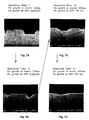
- Figure 1 shows scanning electron micrograph cross-sections of the selective oxide deposition using a 391 second deposition time on a patterned wafer without pretreatment ( Figure 1A ) with an oxide thickness of 2420 ⁇ on SiN and 6290 ⁇ on Si, with H202 pretreament ( Figure 1B ) with an oxide thickness of 290 ⁇ on SiN and 4260 ⁇ on Si and with isopropanol alcohol (IPA) pretreament ( Figure 1C ) with an oxide thickness of 970 ⁇ on SiN and 5900 ⁇ on Si.
- Figure 1A shows scanning electron micrograph cross-sections of the selective oxide deposition using a 391 second deposition time on a patterned wafer without pretreatment
- Figure 1B with an oxide thickness of 290 ⁇ on SiN and 4260 ⁇ on Si
- IPA isopropanol alcohol
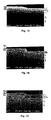
- Figure 2 shows scanning electron micrograph cross-sections of the surface morphology of SiO 2 on untreated SiN film ( Fig. 2A ), on H2O2-pretreated SiN film ( Fig. 2B ) and on either IPA- or acetone-pretreated SiN ( Fig. 2C ).
- Figure 3 depicts the oxide film thickness on bare silicon, silicon nitride and H2O2-pretreated silicon nitride substrates with different 03:TEOS flow ratios. Flow ratios are changed by changing the wt%O3 flow. Deposition time was 352 seconds for each wafer.
- FIG 4 compares diagrammatic and scanning electron micrographs of shallow trench isolation deposition techniques for traditional sub-atmospheric chemical vapor oxide deposition (SACVD), atmospheric pressure chemical vapor oxide deposition (APCVD) and low pressure chemical vapor oxide deposition (LPCVD) ( Figure 4A ); high density plasma chemical vapor oxide deposition (HDPCVD) ( Figure 4B); and sub-atmospheric chemical vapor selective oxide deposition (SELOX SACVD) ( Figure 4C ).
- SACVD sub-atmospheric chemical vapor oxide deposition
- APCVD atmospheric pressure chemical vapor oxide deposition
- LPCVD low pressure chemical vapor oxide deposition
- SELOX SACVD sub-atmospheric chemical vapor selective oxide deposition
- Selective oxide deposition enables easy chemical mechanical polishing (CMP) integration as it is not necessary to use dummy features or inverse masking.
- Figure 5 depicts a cross-sectional view of a wafer after SACVD selective oxidation for trench fill including thermal electron micrographs (TEM) of the corners of the wafer.
- TEM thermal electron micrographs
- Figure 6 compares oxide deposition on silicon nitride and silicon as a function of time.
- Figure 7 shows scanning electron micrographs depicting the delayed nucleation effect of oxide on a silicon nitride pad layer as compared to the oxide growth on silicon in the trench of the wafer.
- oxide growth in trench is 100 n m and oxide growth on SiN is negligible ( Figure 7A ); at time 2t, oxide growth in trench is 200 n m and oxide growth on SiN is negligible ( Figure 7B ); at time 4t, oxide growth in trench is 400 nm and oxide growth on SiN is 150 nm ( Figure 7C ); and at time 8t, oxide growth in trench is 850 n m and oxide growth on SiN is 450 n m ( Figure 7D ).
- Figure 8 depicts the optimization of pressure, temperature and O3/TEOS ratio for specific selectivities for conformal and selective SACVD deposition of oxide films.
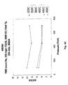
- Figure 9 illustrates characteristics of the SELOX process as performed using SACVD as a function of pressure and temperture.
- Selectivity process conditions of 7000 sccm He, 350 mgm TEOS, 5000 O 3 (15 wt%), 230 mils, 5000 ⁇ film ( Figure 9A ); Deposition Rate: process conditions of 7000 sccm He, 350 mgm TEOS, 5000 O 3 (15 wt%), 230 mils, 5000 ⁇ film ( Figure 9B ); Wet Etch Rate Ratio (WERR) process conditions of 7000 sccm He, 350 mgm TEOS, 5000 O 3 (15 wt%), 230 mils, 5000 ⁇ film ( Figure 9C ); Shrinkage: process conditions of 7000 sccm He, 350 mgm TEOS, 5000 O 3 (15wt%), 230 mils, 1000C anneal, 30 min., N 2 ( Figure 9D ); Clean Time: process conditions of 7000 sccm He, 350 mg
- a method of decreasing a deposition rate of a silicon dioxide film on a silicon nitride pad on a wafer comprising the steps of pretreating the wafer and vapor-depositing a silicon dioxide film on the wafer.
- the decreased silicon dioxide deposition rate on the silicon nitride substrate results in a self-planarizing silicon dioxide trench fill on the wafer wherein selectivity remains constant with a change in film thickness.
- the wafers employed may be, for example, shallow trench isolation devices comprising a silicon substrate and a silicon nitride pad.
- the pretreating step may comprise the steps of contacting the wafer with a chemical compound and air-drying the chemical compound on the wafer.
- Representative examples of chemical compounds which can be used to air dry the wafer include hydrogen peroxide, isopropyl alcohol and acetone. Additionally, the hydrogen peroxide may comprise a 30% solution in water.
- the silicon dioxide film is deposited on the wafer by a selective oxidation sub-atmospheric chemical vapor deposition (SELOX SACVD) process.
- SELOX SACVD selective oxidation sub-atmospheric chemical vapor deposition
- a representative example of the SELOX SACVD process uses an ozone activated tetraethylorthosilicate (O3/TEOS) process to deposit the silicon dioxide on the wafer.
- O3/TEOS ozone activated tetraethylorthosilicate
- the temperature selected during the selective oxidation sub-atmospheric chemical vapor deposition of silicon dioxide on the wafer may be, for example, about 400 °C.
- a method of pretreating a wafer prior to depositing a silicon dioxide film on the wafer comprises the steps of contacting the wafer with a chemical compound and air-drying the chemical compound onto the wafer.
- the pretreatment of the wafer decreases the deposition rate of a silicon dioxide film on a silicon nitride pad on the wafer and the selectivity remains constant with a change in film thickness.
- Representative examples of chemical compounds which are useful in air drying the wafer in this method include hydrogen peroxide, isopropyl alcohol and acetone. Additionally, the hydrogen peroxide may comprise a 30% solution in water.
- the wafers employed may be, for example, shallow trench isolation devices comprising a silicon substrate and a silicon nitride pad.
- the silicon dioxide film is deposited on the wafer by a selective oxidation sub-atmospheric chemical vapor deposition (SELOX SACVD) process.
- SELOX SACVD selective oxidation sub-atmospheric chemical vapor deposition
- a representative example of the SELOX SACVD process uses an ozone activated tetraethylorthosilicate (O3/TEOS) process to deposit the silicon dioxide on the wafer.
- O3/TEOS ozone activated tetraethylorthosilicate
- a useful temperature selected during the selective oxidation sub-atmospheric chemical vapor deposition of silicon dioxide on the wafer may be, for example, about 400 °C.
- a method of decreasing a deposition rate of a silicon dioxide film on a silicon nitride pad on a shallow trench isolation silicon wafer comprises the steps of contacting the wafer with a 30% hydrogen peroxide solution in water; air-drying the hydrogen peroxide solution onto the wafer; and vapor depositing the silicon dioxide on the wafer using ozone activated tetraethylorthosilicate (O 3 /TEOS) wherein the vapor deposition is a selective oxidation sub-atmospheric chemical vapor deposition process (SELOX SACVD).
- SELOX SACVD selective oxidation sub-atmospheric chemical vapor deposition process
- the decreased silicon dioxide deposition rate on the silicon nitride pad results in a self-planarizing silicon dioxide trench fill on the wafer such that selectivity remains constant with a change in film thickness.
- a useful temperature employed during the selective oxidation sub-atmospheric chemical vapor deposition of silicon dioxide on the wafer may be, for example, about 400 °C.
- SACVDTM selective oxide deposition of silicon oxide for shallow trench isolation was carried out using AMAT Giga-Fill SACVDTM USG equipment.
- CMP chemical-mechanical polishing
- Pretreatment allows for a much higher selectivity which improves the overall process.
- a sufficient film thickness multiple or selectivity which is defined as SiO 2 thickness on Si/SiO 2 thickness on SiN, varies based on, among other considerations, the trench geometry, SiN thickness, CMP procedure.
- the ability to increase the multiple removes the need for subsequent planarization steps and decreases the time required for CMP resulting in an increased wafer throughput. It also improves the quality of the silicon dioxide film on silicon nitride; i.e., the resultant film is denser than without pretreatment.
- the improved quality of the film allows for nondestructive means; such as ellipsometry, of measuring its thickness allowing for a more accurate end point of the CMP process, thereby making the overall module
- the selective deposition process is carried out at lower temperatures thus increasing the deposition rate and therefore throughput.
- the deposition rate of the selective process is 90nm/min on silicon at 430 °C versus 140 n m/min on silicon at 400 °C.
- the best known method is at 400 °C versus 430 °C for the untreated standard selective process.
- the elevated deposition temperature prevents the porous silicon dioxide film on silicon nitride from encroaching into the trench areas at the silicon "corner" region.
- the selectivity or film thickness multiple becomes independent of silicon dioxide thickness with the pretreatment method.
- pretreatment the deposition rate of silicon dioxide on silicon nitride is no longer delayed; however, the deposition rate on silicon nitride is much reduced relative to silicon while not affecting the deposition rate on silicon. This allows for a more predictable process when going to smaller, more aggressive trench geometries.
- Silicon dioxide film thickness on silicon is measured in large open areas; i.e., areas that have had silicon etched without an active area nearby. Silicon dioxide film thickness on silicon nitride is measured in larger active areas; i.e., areas that do not have etched areas nearby and have the silicon nitride pad intact.
- FIGS. 1A and 1B show scanning electron micrograph (SEM) cross-sections of patterned wafers deposited by the same O 3 /TEOS process.
- Oxide deposition on a patterned wafer without pretreatment yields a film thickness multiple of 2.6x. With H 2 O 2 pretreatment, the multiple increases to 14.7x. Filling of the trench with oxide is not affected by the H 2 O 2 pretreatment. While the oxide deposition rate has decreased somewhat on Si with H 2 O 2 pretreatment, it is significantly decreased on SiN.
- Oxide film thickness with acetone-pretreatment of flat wafers is similar to the deposition thickness and film morphology of patterned wafers with IPA-pretreatment (data not shown).
- the morphology of the SiO 2 film grown on SiN with H 2 O 2 -pretreatment is different than on untreated SiN.
- Oxide films on H 2 O 2 -pretreated SiN are smoother; i.e., they do not have any pores (Figs. 2A and 2B).
- Oxide film thickness measurement on SiN is crucial to determine the time for chemical mechanical polishing in the subsequent step.
- pretreatment by either IPA or acetone did not achieve the high selectivity of H 2 O 2 -pretreatment.
- the film quality also improved with either IPA or acetone pretreatment, but again not to the degree H 2 O 2 -pretreatment improved subsequent oxide film quality (Fig. 2C). Therefore, pretreatment by H 2 O 2 represents the best known method for enhancing selectivity with the current oxide deposition process.
- Selective oxide deposition for shallow trench isolation provides a tunable selectivity between the oxide growth rate on silicon and the oxide growth rate on silicon nitride to achieve a self-planarizing oxide growth.
- Selectivity film thickness on silicon film thickness on nitride where the film thickness on silicon is greater than the film thickness on silicon nitride.
- Figure 3 shows the change in film thickness on silicon nitride and silicon (flat) wafers with different O 3 :TEOS ratios. Decreased film thicknesses are observed over the range of O 3 :TEOS flow ratios examined, although the difference decreased with decreasing ratios.
- corner rounding is achieved by high temperature oxygen deposition that grows a thermal oxide.
- the SELOX process can attain the same good corner rounding as other vapor deposition processes such as high density plasma (HDP) vapor deposition.
- HDP high density plasma
- the post trench fill oxidation after a 150 ⁇ thermal oxide grown after a 1050°C, 45 minute anneal in O 2 , shows good corner rounding with a homogeneous covering of oxide and no negative effect on the silicon wafer (Fig. 5).
- the selectivity of the standard SACVD O 3 /TEOS film deposition is utilized to achieve self-planarization of the oxide layer as it is deposited on the wafer.
- selectivity is due to delayed nucleation of silicon dioxide on the silicon nitride pad as compared to the more immediate nucleation of silicon dioxide on the silicon in the trench. Once nucleation on nitride is initiated, however, the rate of oxide deposition is similar to that of oxide deposition on silicon in the trench when measuring film thickness.
- silicon dioxide deposited on silicon nitride is porous as compared to that on silicon, it effectively appears that the deposition rate on silicon nitride is reduced; i.e., not as many silicon dioxide molecules are deposited on silicon nitride as on silicon even though the film thickness on each are similar.
- the graph in Figure 6 indicates that, although oxide deposition onto the silicon in the trench of the wafer occurs immediately, oxide growth on the silicon nitride pad does not occur until a deposition time of 2t. This delayed nucleation effect coupled with the slightly faster rate of oxide deposition on silicon results in a self-planarized silicon dioxide layer on the wafer by a time of 8t.
- the scanning electron micrographs in Figure 7 demonstrate that no significant oxide deposition on silicon nitride is even visible until a deposition time of 4t (Fig. 7C).
- pretreatment of the wafers With pretreatment of the wafers, delayed nucleation of silicon dioxide on silicon nitride no longer occurs. While the deposition rate on silicon is unchanged, the deposition rate on silicon nitride is markedly reduced.
- pretreatment of the wafer results in an unchanged selectivity no matter what silicon dioxide thickness is deposited whereas, absent pretreatment, the selectivity value changes with silicon dioxide film thickness during the standard SELOX SACVD process.
- An ozone-activated TEOS deposition of silicon dioxide films on the silicon nitride/silicon wafer is used to achieve self-planarization prior to chemical mechanical polishing of the wafer.
- a selective oxide deposition process the initial step height of the trench is compensated for by choosing a selectivity value and determining the deposition time required for a globally planar oxide surface on the wafer.
- Pressure, temperature and O 3 /TEOS ratio are optimized for either conformal SACVD USG oxide deposition for selectivity values of approximately 1 or selective SACVD USG deposition for selectivity values greater than 1 (Fig. 8).
- the ozone/TEOS process possesses several advantages with reference to process integration. For example, a tunable selectivity/deposition rate results in more global self-planarization (Figs. 9A and 9B), the shrinkage of the ozone/TEOS/oxide after annealing is minimal (Fig. 9D), and a void-free gap fill is achieved for very small gaps ( ⁇ 0.1 micron trench opening). Pretreatment enables increased deposition rate with lower temperatures. As the SELOX process does not require as many post deposition process steps as other shallow trench isolation procedures, the complexity and overall cost are reduced and wafer throughtput is increased.
- Table 1 summarizes the results of O 3 /TEOS deposition of oxide film on a wafer under process conditions of variable temperature, pressure and O 3 /TEOS ratios. Optimal conditions are 430C, 700 torr and 17wt% O 3 which yield a good film quality below the nitride level.
- Table 2 summarizes the results using optimal conditions of silicon dioxide deposition using conformal deposition techniques, the standard shallow trench SELOX process and the new shallow trench SELOX process employing pretreatment of wafers. The new SELOX process shows good film quality next to the nitride layer at a deposition rate of 1400 ⁇ /min.
Landscapes
- Chemical & Material Sciences (AREA)
- General Chemical & Material Sciences (AREA)
- Chemical Kinetics & Catalysis (AREA)
- Engineering & Computer Science (AREA)
- Materials Engineering (AREA)
- Mechanical Engineering (AREA)
- Metallurgy (AREA)
- Organic Chemistry (AREA)
- Inorganic Chemistry (AREA)
- Element Separation (AREA)
- Formation Of Insulating Films (AREA)
Abstract
Description

| PRETREATMENT | |||
| DxZ ILD | ST SELOX | + | |
| 385C, 450Torr 12.5 | 430C, 700Torr | 400C, 700Torr | |
| Deposition Å/min Rate | 2029 Å/min | 1400 Å/min | 1400 |
| Uniformity 49 pt. sigma | 1.92% | 4.8% | 3.3% |
| Selectivity Si:Nitride | 1.3 | 2.6 | > 5 |
| WERR (as dep) | 4,8 | 3,6 | |
| WERR post anneal | 1.4 | 1.4 | |
| Shrinkage N2, 1000C | 5 | 3 | |
| Shrinkage 02, | 1 | 1 | |
| Film quality below nitride | poor and porous | good no voids | good no voids |
Claims (11)
- A method of decreasing the deposition rate of a silicon dioxide film on a silicon nitride pad on a wafer, the method comprising the steps of:pretreating said wafer; andvapour-depositing a silicon dioxide film on said wafer; wherein a decreased silicon dioxide deposition rate on the silicon nitride substrate results in a self-planarizing silicon dioxide trench fill on said wafer.
- The method of claim 1, wherein said pretreating step comprises the steps of:contracting said wafer with a chemical compound selected from one or more of hydrogen peroxide, isopropyl alcohol and acetone; andair-drying said chemical compound on said wafer.
- A method of pretreating a wafer prior to depositing a silicon dioxide film on said wafer, the method comprising the steps of:wherein said pretreatment of said wafer decreases a deposition rate of a silicon dioxide film on a silicon nitride pad on said wafer.contacting said wafer with a chemical compound selected from one or more of hydrogen peroxide, isopropyl alcohol and acetone; andair-drying said chemical compound onto said wafer;
- The method of any one of the preceding claims, wherein said wafer comprises a shallow trench isolation device.
- The method of any one of the preceding claims, wherein said wafer comprises a silicon substrate and a silicon nitride pad.
- The method of any one of claims 2 to 5, wherein said hydrogen peroxide comprises a 30% solution in water.
- The method of any one of the preceding claims, wherein said silicon dioxide film is deposited on said wafer by a selective oxidation sub-atmospheric chemical vapour deposition (SELOX SACVD) process.
- The method of claim 7, wherein said selective oxidation sub-atmospheric chemical vapour deposition (SELOX SACVD) uses an ozone activated tetraethylorthosilicate (O3/TEOS) process to deposit said silicon dioxide on said wafer.
- A method of decreasing the deposition rate of a silicon dioxide film on a silicon nitride pad on a shallow trench isolation silicon wafer, the method comprising the steps of:contacting said wafer with a 30% hydrogen peroxide solution in water;air-drying said hydrogen peroxide solution onto said wafer; andvapour depositing said silicon dioxide on said wafer using ozone activated tetraethylorthosilicate (O3/TEOS), wherein said vapour deposition is a selective oxidation sub-atmospheric chemical vapour deposition process (SELOX SACVD), and wherein a decreased silicon dioxide deposition rate on the silicon nitride pad results in a self-planarizing silicon dioxide trench fill on said wafer.
- The method of any one of the preceding claims, wherein selectivity remains constant with a change in film thickness.
- The method of any one of the preceding claims, wherein said silicon dioxide is deposited on said wafer at a temperature of 400°C.
Applications Claiming Priority (2)
| Application Number | Priority Date | Filing Date | Title |
|---|---|---|---|
| US629040 | 2000-07-31 | ||
| US09/629,040 US6541401B1 (en) | 2000-07-31 | 2000-07-31 | Wafer pretreatment to decrease rate of silicon dioxide deposition on silicon nitride compared to silicon substrate |
Publications (3)
| Publication Number | Publication Date |
|---|---|
| EP1178528A2 true EP1178528A2 (en) | 2002-02-06 |
| EP1178528A3 EP1178528A3 (en) | 2010-04-28 |
| EP1178528B1 EP1178528B1 (en) | 2012-01-11 |
Family
ID=24521341
Family Applications (1)
| Application Number | Title | Priority Date | Filing Date |
|---|---|---|---|
| EP01306570A Expired - Lifetime EP1178528B1 (en) | 2000-07-31 | 2001-07-31 | Wafer pretreatment to decrease the deposition rate of silicon dioxide on silicon nitride in comparison to its deposition rate on a silicon substrate |
Country Status (6)
| Country | Link |
|---|---|
| US (1) | US6541401B1 (en) |
| EP (1) | EP1178528B1 (en) |
| JP (1) | JP5128033B2 (en) |
| KR (1) | KR100801363B1 (en) |
| AT (1) | ATE541305T1 (en) |
| TW (1) | TW519692B (en) |
Cited By (3)
| Publication number | Priority date | Publication date | Assignee | Title |
|---|---|---|---|---|
| DE102004042459B3 (en) * | 2004-08-31 | 2006-02-09 | Infineon Technologies Ag | A method of making a high aspect ratio trench isolation structure |
| KR100801363B1 (en) * | 2000-07-31 | 2008-02-05 | 어플라이드 머티어리얼스, 인코포레이티드 | Wafer pretreatment method for reducing silicon dioxide deposition rate on silicon nitride on silicon substrate |
| CN102856175A (en) * | 2012-09-19 | 2013-01-02 | 上海华力微电子有限公司 | Furnace tube retaining plate structure and manufacturing method thereof |
Families Citing this family (51)
| Publication number | Priority date | Publication date | Assignee | Title |
|---|---|---|---|---|
| US7069101B1 (en) | 1999-07-29 | 2006-06-27 | Applied Materials, Inc. | Computer integrated manufacturing techniques |
| US6640151B1 (en) * | 1999-12-22 | 2003-10-28 | Applied Materials, Inc. | Multi-tool control system, method and medium |
| US7188142B2 (en) | 2000-11-30 | 2007-03-06 | Applied Materials, Inc. | Dynamic subject information generation in message services of distributed object systems in a semiconductor assembly line facility |
| US7698012B2 (en) | 2001-06-19 | 2010-04-13 | Applied Materials, Inc. | Dynamic metrology schemes and sampling schemes for advanced process control in semiconductor processing |
| US7201936B2 (en) * | 2001-06-19 | 2007-04-10 | Applied Materials, Inc. | Method of feedback control of sub-atmospheric chemical vapor deposition processes |
| US6910947B2 (en) * | 2001-06-19 | 2005-06-28 | Applied Materials, Inc. | Control of chemical mechanical polishing pad conditioner directional velocity to improve pad life |
| US7101799B2 (en) | 2001-06-19 | 2006-09-05 | Applied Materials, Inc. | Feedforward and feedback control for conditioning of chemical mechanical polishing pad |
| US20020192966A1 (en) * | 2001-06-19 | 2002-12-19 | Shanmugasundram Arulkumar P. | In situ sensor based control of semiconductor processing procedure |
| US6913938B2 (en) | 2001-06-19 | 2005-07-05 | Applied Materials, Inc. | Feedback control of plasma-enhanced chemical vapor deposition processes |
| US7047099B2 (en) * | 2001-06-19 | 2006-05-16 | Applied Materials Inc. | Integrating tool, module, and fab level control |
| US7160739B2 (en) * | 2001-06-19 | 2007-01-09 | Applied Materials, Inc. | Feedback control of a chemical mechanical polishing device providing manipulation of removal rate profiles |
| US7082345B2 (en) * | 2001-06-19 | 2006-07-25 | Applied Materials, Inc. | Method, system and medium for process control for the matching of tools, chambers and/or other semiconductor-related entities |
| US7337019B2 (en) | 2001-07-16 | 2008-02-26 | Applied Materials, Inc. | Integration of fault detection with run-to-run control |
| US6950716B2 (en) * | 2001-08-13 | 2005-09-27 | Applied Materials, Inc. | Dynamic control of wafer processing paths in semiconductor manufacturing processes |
| US20030037090A1 (en) * | 2001-08-14 | 2003-02-20 | Koh Horne L. | Tool services layer for providing tool service functions in conjunction with tool functions |
| US6984198B2 (en) * | 2001-08-14 | 2006-01-10 | Applied Materials, Inc. | Experiment management system, method and medium |
| DE10143997B4 (en) * | 2001-09-07 | 2006-12-14 | Infineon Technologies Ag | Method for producing a semiconductor integrated circuit with an isolation trench |
| US20040018735A1 (en) * | 2002-05-21 | 2004-01-29 | Park Seung G. | Method of depositing an oxide film by chemical vapor deposition |
| US7668702B2 (en) * | 2002-07-19 | 2010-02-23 | Applied Materials, Inc. | Method, system and medium for controlling manufacturing process using adaptive models based on empirical data |
| KR20050026099A (en) * | 2002-08-01 | 2005-03-14 | 어플라이드 머티어리얼즈 인코포레이티드 | Method, system, and medium for handling misrepresentative metrology data within an advanced process control system |
| US20040063224A1 (en) * | 2002-09-18 | 2004-04-01 | Applied Materials, Inc. | Feedback control of a chemical mechanical polishing process for multi-layered films |
| US7141483B2 (en) * | 2002-09-19 | 2006-11-28 | Applied Materials, Inc. | Nitrous oxide anneal of TEOS/ozone CVD for improved gapfill |
| US7456116B2 (en) | 2002-09-19 | 2008-11-25 | Applied Materials, Inc. | Gap-fill depositions in the formation of silicon containing dielectric materials |
| US7335609B2 (en) * | 2004-08-27 | 2008-02-26 | Applied Materials, Inc. | Gap-fill depositions introducing hydroxyl-containing precursors in the formation of silicon containing dielectric materials |
| US20070212850A1 (en) * | 2002-09-19 | 2007-09-13 | Applied Materials, Inc. | Gap-fill depositions in the formation of silicon containing dielectric materials |
| US7431967B2 (en) * | 2002-09-19 | 2008-10-07 | Applied Materials, Inc. | Limited thermal budget formation of PMD layers |
| TW556316B (en) * | 2002-09-25 | 2003-10-01 | Nanya Technology Corp | A method of fabricating a shallow trench isolation with high aspect ratio |
| US7272459B2 (en) * | 2002-11-15 | 2007-09-18 | Applied Materials, Inc. | Method, system and medium for controlling manufacture process having multivariate input parameters |
| US7333871B2 (en) * | 2003-01-21 | 2008-02-19 | Applied Materials, Inc. | Automated design and execution of experiments with integrated model creation for semiconductor manufacturing tools |
| DE10314574B4 (en) * | 2003-03-31 | 2007-06-28 | Infineon Technologies Ag | Method for producing a trench isolation structure |
| US7205228B2 (en) * | 2003-06-03 | 2007-04-17 | Applied Materials, Inc. | Selective metal encapsulation schemes |
| US7354332B2 (en) | 2003-08-04 | 2008-04-08 | Applied Materials, Inc. | Technique for process-qualifying a semiconductor manufacturing tool using metrology data |
| US7356377B2 (en) | 2004-01-29 | 2008-04-08 | Applied Materials, Inc. | System, method, and medium for monitoring performance of an advanced process control system |
| US6961626B1 (en) | 2004-05-28 | 2005-11-01 | Applied Materials, Inc | Dynamic offset and feedback threshold |
| US7096085B2 (en) | 2004-05-28 | 2006-08-22 | Applied Materials | Process control by distinguishing a white noise component of a process variance |
| US20070212847A1 (en) * | 2004-08-04 | 2007-09-13 | Applied Materials, Inc. | Multi-step anneal of thin films for film densification and improved gap-fill |
| US7642171B2 (en) * | 2004-08-04 | 2010-01-05 | Applied Materials, Inc. | Multi-step anneal of thin films for film densification and improved gap-fill |
| US7547621B2 (en) * | 2006-07-25 | 2009-06-16 | Applied Materials, Inc. | LPCVD gate hard mask |
| JP2009099909A (en) * | 2007-10-19 | 2009-05-07 | Toshiba Corp | Manufacturing method of semiconductor device |
| US20090176368A1 (en) * | 2008-01-08 | 2009-07-09 | Nan Wu | Manufacturing method for an integrated circuit structure comprising a selectively deposited oxide layer |
| US20090194810A1 (en) * | 2008-01-31 | 2009-08-06 | Masahiro Kiyotoshi | Semiconductor device using element isolation region of trench isolation structure and manufacturing method thereof |
| JP2009182270A (en) * | 2008-01-31 | 2009-08-13 | Toshiba Corp | Semiconductor device and manufacturing method thereof |
| CN101989564B (en) * | 2009-07-31 | 2012-09-26 | 中芯国际集成电路制造(上海)有限公司 | Method for reducing corner defect of isolation channel of shallow trench |
| JP6060460B2 (en) * | 2012-11-22 | 2017-01-18 | アーゼット・エレクトロニック・マテリアルズ(ルクセンブルグ)ソシエテ・ア・レスポンサビリテ・リミテ | Method for forming siliceous film and siliceous film formed by the same method |
| US9018108B2 (en) | 2013-01-25 | 2015-04-28 | Applied Materials, Inc. | Low shrinkage dielectric films |
| JP2016025195A (en) | 2014-07-18 | 2016-02-08 | 東京エレクトロン株式会社 | Etching method |
| JP6494226B2 (en) * | 2014-09-16 | 2019-04-03 | 東京エレクトロン株式会社 | Etching method |
| JP6893613B2 (en) * | 2015-04-13 | 2021-06-23 | 東京エレクトロン株式会社 | Systems and methods for flattening substrates |
| WO2016209570A1 (en) * | 2015-06-26 | 2016-12-29 | Applied Materials, Inc. | Selective deposition of silicon oxide films |
| US9991133B2 (en) * | 2016-08-11 | 2018-06-05 | Tokyo Electron Limited | Method for etch-based planarization of a substrate |
| US11211272B2 (en) | 2019-09-25 | 2021-12-28 | Micron Technology, Inc. | Contaminant detection tools and related methods |
Family Cites Families (19)
| Publication number | Priority date | Publication date | Assignee | Title |
|---|---|---|---|---|
| US5190792A (en) * | 1989-09-27 | 1993-03-02 | International Business Machines Corporation | High-throughput, low-temperature process for depositing oxides |
| JPH0779127B2 (en) * | 1989-12-27 | 1995-08-23 | 株式会社半導体プロセス研究所 | Method for manufacturing semiconductor device |
| JP2812599B2 (en) * | 1992-02-06 | 1998-10-22 | シャープ株式会社 | Method for manufacturing semiconductor device |
| EP0560617A3 (en) * | 1992-03-13 | 1993-11-24 | Kawasaki Steel Co | Method of manufacturing insulating film on semiconductor device and apparatus for carrying out the same |
| JPH06283523A (en) * | 1993-03-26 | 1994-10-07 | Kawasaki Steel Corp | Manufacture of semiconductor device |
| JPH06283506A (en) * | 1993-03-26 | 1994-10-07 | Kawasaki Steel Corp | Method for manufacturing semiconductor device |
| JPH0945687A (en) * | 1995-07-26 | 1997-02-14 | Ricoh Co Ltd | Substrate surface flattening method |
| KR0179554B1 (en) * | 1995-11-30 | 1999-04-15 | 김주용 | Device isolation insulating film formation method of semiconductor device |
| JPH1022284A (en) * | 1996-06-28 | 1998-01-23 | Toshiba Corp | Semiconductor device and manufacturing method thereof |
| DE19629766C2 (en) * | 1996-07-23 | 2002-06-27 | Infineon Technologies Ag | Manufacturing method of shallow trench isolation areas in a substrate |
| JPH10294311A (en) * | 1997-04-18 | 1998-11-04 | Matsushita Electron Corp | Method for manufacturing semiconductor device |
| KR100546265B1 (en) * | 1997-08-27 | 2006-03-23 | 삼성전자주식회사 | Fabrication method of polysilicon thin film transistor |
| JP3315907B2 (en) * | 1997-10-24 | 2002-08-19 | 松下電器産業株式会社 | Method for manufacturing semiconductor device |
| JP2953447B2 (en) * | 1997-11-14 | 1999-09-27 | 日本電気株式会社 | Manufacturing method of groove-separated semiconductor device |
| US6413583B1 (en) * | 1998-02-11 | 2002-07-02 | Applied Materials, Inc. | Formation of a liquid-like silica layer by reaction of an organosilicon compound and a hydroxyl forming compound |
| JP2000068367A (en) * | 1998-08-19 | 2000-03-03 | Hitachi Ltd | Method for manufacturing semiconductor integrated circuit device |
| KR100297737B1 (en) * | 1998-09-24 | 2001-11-01 | 윤종용 | Trench Isolation Method of Semiconductor Device |
| US6235354B1 (en) * | 1999-11-01 | 2001-05-22 | United Microelectronics Corp. | Method of forming a level silicon oxide layer on two regions of different heights on a semiconductor wafer |
| US6541401B1 (en) * | 2000-07-31 | 2003-04-01 | Applied Materials, Inc. | Wafer pretreatment to decrease rate of silicon dioxide deposition on silicon nitride compared to silicon substrate |
-
2000
- 2000-07-31 US US09/629,040 patent/US6541401B1/en not_active Expired - Lifetime
-
2001
- 2001-07-31 AT AT01306570T patent/ATE541305T1/en active
- 2001-07-31 EP EP01306570A patent/EP1178528B1/en not_active Expired - Lifetime
- 2001-07-31 KR KR1020010046342A patent/KR100801363B1/en not_active Expired - Fee Related
- 2001-07-31 TW TW090118691A patent/TW519692B/en not_active IP Right Cessation
- 2001-07-31 JP JP2001232055A patent/JP5128033B2/en not_active Expired - Fee Related
Cited By (5)
| Publication number | Priority date | Publication date | Assignee | Title |
|---|---|---|---|---|
| KR100801363B1 (en) * | 2000-07-31 | 2008-02-05 | 어플라이드 머티어리얼스, 인코포레이티드 | Wafer pretreatment method for reducing silicon dioxide deposition rate on silicon nitride on silicon substrate |
| DE102004042459B3 (en) * | 2004-08-31 | 2006-02-09 | Infineon Technologies Ag | A method of making a high aspect ratio trench isolation structure |
| US7393756B2 (en) | 2004-08-31 | 2008-07-01 | Infineon Technologies Ag | Method for fabricating a trench isolation structure having a high aspect ratio |
| CN102856175A (en) * | 2012-09-19 | 2013-01-02 | 上海华力微电子有限公司 | Furnace tube retaining plate structure and manufacturing method thereof |
| CN102856175B (en) * | 2012-09-19 | 2015-08-19 | 上海华力微电子有限公司 | Boiler tube baffle structure manufacture method |
Also Published As
| Publication number | Publication date |
|---|---|
| EP1178528B1 (en) | 2012-01-11 |
| JP5128033B2 (en) | 2013-01-23 |
| EP1178528A3 (en) | 2010-04-28 |
| KR100801363B1 (en) | 2008-02-05 |
| KR20020019877A (en) | 2002-03-13 |
| US6541401B1 (en) | 2003-04-01 |
| ATE541305T1 (en) | 2012-01-15 |
| JP2002151510A (en) | 2002-05-24 |
| TW519692B (en) | 2003-02-01 |
Similar Documents
| Publication | Publication Date | Title |
|---|---|---|
| US6541401B1 (en) | Wafer pretreatment to decrease rate of silicon dioxide deposition on silicon nitride compared to silicon substrate | |
| US6180490B1 (en) | Method of filling shallow trenches | |
| JP2002151510A5 (en) | ||
| JP2738831B2 (en) | Method for forming field oxide film of semiconductor device | |
| US5726090A (en) | Gap-filling of O3 -TEOS for shallow trench isolation | |
| US4885262A (en) | Chemical modification of spin-on glass for improved performance in IC fabrication | |
| JP3568537B2 (en) | Electron beam processed film for microelectronic structure | |
| EP1094506A2 (en) | Capping layer for extreme low dielectric constant films | |
| US6207554B1 (en) | Gap filling process in integrated circuits using low dielectric constant materials | |
| KR19990067866A (en) | Semicondustor device with low permittivity interlayer insulating film and method of manufacturing the same | |
| JP3827056B2 (en) | Method for forming interlayer insulating film and semiconductor device | |
| US20040169005A1 (en) | Methods for forming a thin film on an integrated circuit including soft baking a silicon glass film | |
| US7125794B2 (en) | Method of manufacturing semiconductor device | |
| US6235608B1 (en) | STI process by method of in-situ multilayer dielectric deposition | |
| EP1081755A2 (en) | Method for improving a quality of dielectric layer and semiconductor device | |
| US6294473B1 (en) | Method of polishing substrates comprising silicon dioxide and composition relating thereto | |
| KR100334245B1 (en) | Method of forming a device isolation region | |
| JPH10189578A (en) | Method for manufacturing semiconductor device | |
| KR100213204B1 (en) | Method for forming thin film of semiconductor device | |
| KR100437541B1 (en) | Device isolation insulating film formation method of semiconductor device | |
| KR100802240B1 (en) | Device Separation Method for Semiconductor Devices Using Inverse Selectivity Slurry | |
| KR100639886B1 (en) | US deposition method using gap fill of semiconductor device | |
| KR100234370B1 (en) | Method of manufacturing semiconductor device | |
| KR100623595B1 (en) | Planarization method of interlayer insulating film of semiconductor device | |
| CN1383201A (en) | Method for manufacturing shallow groove isolation structure |
Legal Events
| Date | Code | Title | Description |
|---|---|---|---|
| PUAI | Public reference made under article 153(3) epc to a published international application that has entered the european phase |
Free format text: ORIGINAL CODE: 0009012 |
|
| AK | Designated contracting states |
Kind code of ref document: A2 Designated state(s): AT BE CH CY DE DK ES FI FR GB GR IE IT LI LU MC NL PT SE TR |
|
| AX | Request for extension of the european patent |
Free format text: AL;LT;LV;MK;RO;SI |
|
| PUAL | Search report despatched |
Free format text: ORIGINAL CODE: 0009013 |
|
| AK | Designated contracting states |
Kind code of ref document: A3 Designated state(s): AT BE CH CY DE DK ES FI FR GB GR IE IT LI LU MC NL PT SE TR |
|
| AX | Request for extension of the european patent |
Extension state: AL LT LV MK RO SI |
|
| 17P | Request for examination filed |
Effective date: 20100923 |
|
| 17Q | First examination report despatched |
Effective date: 20101117 |
|
| AKX | Designation fees paid |
Designated state(s): AT BE CH CY DE DK ES FI FR GB GR IE IT LI LU MC NL PT SE TR |
|
| RIC1 | Information provided on ipc code assigned before grant |
Ipc: H01L 21/762 20060101ALI20110323BHEP Ipc: C23C 16/02 20060101ALI20110323BHEP Ipc: H01L 21/316 20060101AFI20110323BHEP |
|
| GRAP | Despatch of communication of intention to grant a patent |
Free format text: ORIGINAL CODE: EPIDOSNIGR1 |
|
| GRAS | Grant fee paid |
Free format text: ORIGINAL CODE: EPIDOSNIGR3 |
|
| GRAA | (expected) grant |
Free format text: ORIGINAL CODE: 0009210 |
|
| AK | Designated contracting states |
Kind code of ref document: B1 Designated state(s): AT BE CH CY DE DK ES FI FR GB GR IE IT LI LU MC NL PT SE TR |
|
| REG | Reference to a national code |
Ref country code: GB Ref legal event code: FG4D |
|
| REG | Reference to a national code |
Ref country code: CH Ref legal event code: EP |
|
| REG | Reference to a national code |
Ref country code: AT Ref legal event code: REF Ref document number: 541305 Country of ref document: AT Kind code of ref document: T Effective date: 20120115 |
|
| REG | Reference to a national code |
Ref country code: IE Ref legal event code: FG4D |
|
| REG | Reference to a national code |
Ref country code: DE Ref legal event code: R096 Ref document number: 60145929 Country of ref document: DE Effective date: 20120308 |
|
| REG | Reference to a national code |
Ref country code: NL Ref legal event code: VDEP Effective date: 20120111 |
|
| PG25 | Lapsed in a contracting state [announced via postgrant information from national office to epo] |
Ref country code: NL Free format text: LAPSE BECAUSE OF FAILURE TO SUBMIT A TRANSLATION OF THE DESCRIPTION OR TO PAY THE FEE WITHIN THE PRESCRIBED TIME-LIMIT Effective date: 20120111 Ref country code: BE Free format text: LAPSE BECAUSE OF FAILURE TO SUBMIT A TRANSLATION OF THE DESCRIPTION OR TO PAY THE FEE WITHIN THE PRESCRIBED TIME-LIMIT Effective date: 20120111 |
|
| PG25 | Lapsed in a contracting state [announced via postgrant information from national office to epo] |
Ref country code: FI Free format text: LAPSE BECAUSE OF FAILURE TO SUBMIT A TRANSLATION OF THE DESCRIPTION OR TO PAY THE FEE WITHIN THE PRESCRIBED TIME-LIMIT Effective date: 20120111 Ref country code: PT Free format text: LAPSE BECAUSE OF FAILURE TO SUBMIT A TRANSLATION OF THE DESCRIPTION OR TO PAY THE FEE WITHIN THE PRESCRIBED TIME-LIMIT Effective date: 20120511 Ref country code: GR Free format text: LAPSE BECAUSE OF FAILURE TO SUBMIT A TRANSLATION OF THE DESCRIPTION OR TO PAY THE FEE WITHIN THE PRESCRIBED TIME-LIMIT Effective date: 20120412 |
|
| REG | Reference to a national code |
Ref country code: AT Ref legal event code: MK05 Ref document number: 541305 Country of ref document: AT Kind code of ref document: T Effective date: 20120111 |
|
| PG25 | Lapsed in a contracting state [announced via postgrant information from national office to epo] |
Ref country code: CY Free format text: LAPSE BECAUSE OF FAILURE TO SUBMIT A TRANSLATION OF THE DESCRIPTION OR TO PAY THE FEE WITHIN THE PRESCRIBED TIME-LIMIT Effective date: 20120111 |
|
| PG25 | Lapsed in a contracting state [announced via postgrant information from national office to epo] |
Ref country code: SE Free format text: LAPSE BECAUSE OF FAILURE TO SUBMIT A TRANSLATION OF THE DESCRIPTION OR TO PAY THE FEE WITHIN THE PRESCRIBED TIME-LIMIT Effective date: 20120111 Ref country code: DK Free format text: LAPSE BECAUSE OF FAILURE TO SUBMIT A TRANSLATION OF THE DESCRIPTION OR TO PAY THE FEE WITHIN THE PRESCRIBED TIME-LIMIT Effective date: 20120111 |
|
| PLBE | No opposition filed within time limit |
Free format text: ORIGINAL CODE: 0009261 |
|
| STAA | Information on the status of an ep patent application or granted ep patent |
Free format text: STATUS: NO OPPOSITION FILED WITHIN TIME LIMIT |
|
| PG25 | Lapsed in a contracting state [announced via postgrant information from national office to epo] |
Ref country code: IT Free format text: LAPSE BECAUSE OF FAILURE TO SUBMIT A TRANSLATION OF THE DESCRIPTION OR TO PAY THE FEE WITHIN THE PRESCRIBED TIME-LIMIT Effective date: 20120111 |
|
| 26N | No opposition filed |
Effective date: 20121012 |
|
| PG25 | Lapsed in a contracting state [announced via postgrant information from national office to epo] |
Ref country code: AT Free format text: LAPSE BECAUSE OF FAILURE TO SUBMIT A TRANSLATION OF THE DESCRIPTION OR TO PAY THE FEE WITHIN THE PRESCRIBED TIME-LIMIT Effective date: 20120111 |
|
| REG | Reference to a national code |
Ref country code: DE Ref legal event code: R097 Ref document number: 60145929 Country of ref document: DE Effective date: 20121012 |
|
| PG25 | Lapsed in a contracting state [announced via postgrant information from national office to epo] |
Ref country code: MC Free format text: LAPSE BECAUSE OF NON-PAYMENT OF DUE FEES Effective date: 20120731 |
|
| REG | Reference to a national code |
Ref country code: CH Ref legal event code: PL |
|
| GBPC | Gb: european patent ceased through non-payment of renewal fee |
Effective date: 20120731 |
|
| REG | Reference to a national code |
Ref country code: FR Ref legal event code: ST Effective date: 20130329 |
|
| PG25 | Lapsed in a contracting state [announced via postgrant information from national office to epo] |
Ref country code: CH Free format text: LAPSE BECAUSE OF NON-PAYMENT OF DUE FEES Effective date: 20120731 Ref country code: LI Free format text: LAPSE BECAUSE OF NON-PAYMENT OF DUE FEES Effective date: 20120731 Ref country code: ES Free format text: LAPSE BECAUSE OF FAILURE TO SUBMIT A TRANSLATION OF THE DESCRIPTION OR TO PAY THE FEE WITHIN THE PRESCRIBED TIME-LIMIT Effective date: 20120422 Ref country code: FR Free format text: LAPSE BECAUSE OF NON-PAYMENT OF DUE FEES Effective date: 20120731 Ref country code: GB Free format text: LAPSE BECAUSE OF NON-PAYMENT OF DUE FEES Effective date: 20120731 |
|
| REG | Reference to a national code |
Ref country code: IE Ref legal event code: MM4A |
|
| PG25 | Lapsed in a contracting state [announced via postgrant information from national office to epo] |
Ref country code: IE Free format text: LAPSE BECAUSE OF NON-PAYMENT OF DUE FEES Effective date: 20120731 |
|
| PGFP | Annual fee paid to national office [announced via postgrant information from national office to epo] |
Ref country code: DE Payment date: 20130731 Year of fee payment: 13 |
|
| PG25 | Lapsed in a contracting state [announced via postgrant information from national office to epo] |
Ref country code: TR Free format text: LAPSE BECAUSE OF FAILURE TO SUBMIT A TRANSLATION OF THE DESCRIPTION OR TO PAY THE FEE WITHIN THE PRESCRIBED TIME-LIMIT Effective date: 20120111 |
|
| PG25 | Lapsed in a contracting state [announced via postgrant information from national office to epo] |
Ref country code: LU Free format text: LAPSE BECAUSE OF NON-PAYMENT OF DUE FEES Effective date: 20120731 |
|
| REG | Reference to a national code |
Ref country code: DE Ref legal event code: R119 Ref document number: 60145929 Country of ref document: DE |
|
| PG25 | Lapsed in a contracting state [announced via postgrant information from national office to epo] |
Ref country code: DE Free format text: LAPSE BECAUSE OF NON-PAYMENT OF DUE FEES Effective date: 20150203 |
|
| REG | Reference to a national code |
Ref country code: DE Ref legal event code: R119 Ref document number: 60145929 Country of ref document: DE Effective date: 20150203 |