EP1178500A1 - Structure intégrée d'inductances à valeurs partagées sur un substrat semiconducteur - Google Patents
Structure intégrée d'inductances à valeurs partagées sur un substrat semiconducteur Download PDFInfo
- Publication number
- EP1178500A1 EP1178500A1 EP01410093A EP01410093A EP1178500A1 EP 1178500 A1 EP1178500 A1 EP 1178500A1 EP 01410093 A EP01410093 A EP 01410093A EP 01410093 A EP01410093 A EP 01410093A EP 1178500 A1 EP1178500 A1 EP 1178500A1
- Authority
- EP
- European Patent Office
- Prior art keywords
- terminal
- inductance
- circuit
- conductive
- mixer
- Prior art date
- Legal status (The legal status is an assumption and is not a legal conclusion. Google has not performed a legal analysis and makes no representation as to the accuracy of the status listed.)
- Granted
Links
Images


Classifications
-
- H—ELECTRICITY
- H01—ELECTRIC ELEMENTS
- H01F—MAGNETS; INDUCTANCES; TRANSFORMERS; SELECTION OF MATERIALS FOR THEIR MAGNETIC PROPERTIES
- H01F21/00—Variable inductances or transformers of the signal type
- H01F21/12—Variable inductances or transformers of the signal type discontinuously variable, e.g. tapped
-
- H—ELECTRICITY
- H01—ELECTRIC ELEMENTS
- H01F—MAGNETS; INDUCTANCES; TRANSFORMERS; SELECTION OF MATERIALS FOR THEIR MAGNETIC PROPERTIES
- H01F17/00—Fixed inductances of the signal type
- H01F17/0006—Printed inductances
-
- H—ELECTRICITY
- H10—SEMICONDUCTOR DEVICES; ELECTRIC SOLID-STATE DEVICES NOT OTHERWISE PROVIDED FOR
- H10W—GENERIC PACKAGES, INTERCONNECTIONS, CONNECTORS OR OTHER CONSTRUCTIONAL DETAILS OF DEVICES COVERED BY CLASS H10
- H10W20/00—Interconnections in chips, wafers or substrates
- H10W20/40—Interconnections external to wafers or substrates, e.g. back-end-of-line [BEOL] metallisations or vias connecting to gate electrodes
- H10W20/497—Inductive arrangements or effects of, or between, wiring layers
-
- H—ELECTRICITY
- H10—SEMICONDUCTOR DEVICES; ELECTRIC SOLID-STATE DEVICES NOT OTHERWISE PROVIDED FOR
- H10W—GENERIC PACKAGES, INTERCONNECTIONS, CONNECTORS OR OTHER CONSTRUCTIONAL DETAILS OF DEVICES COVERED BY CLASS H10
- H10W44/00—Electrical arrangements for controlling or matching impedance
- H10W44/20—Electrical arrangements for controlling or matching impedance at high-frequency [HF] or radio frequency [RF]
-
- H—ELECTRICITY
- H01—ELECTRIC ELEMENTS
- H01F—MAGNETS; INDUCTANCES; TRANSFORMERS; SELECTION OF MATERIALS FOR THEIR MAGNETIC PROPERTIES
- H01F17/00—Fixed inductances of the signal type
- H01F17/0006—Printed inductances
- H01F2017/0046—Printed inductances with a conductive path having a bridge
-
- H—ELECTRICITY
- H01—ELECTRIC ELEMENTS
- H01F—MAGNETS; INDUCTANCES; TRANSFORMERS; SELECTION OF MATERIALS FOR THEIR MAGNETIC PROPERTIES
- H01F21/00—Variable inductances or transformers of the signal type
- H01F21/12—Variable inductances or transformers of the signal type discontinuously variable, e.g. tapped
- H01F2021/125—Printed variable inductor with taps, e.g. for VCO
Definitions
- the present invention relates to inductors with shared values formed on a semiconductor substrate, and particular of such inductors intended to operate in a frequency range greater than several hundred MHz, which we will call here RF range.
- FIG. 1 schematically shows a perspective view inductance L integrated on a substrate semiconductor 1, intended to operate in the RF range.
- the inductance L comprises a conductive track 2 substantially plane deposited on a first insulating layer 5 of the substrate semiconductor.
- the conductive track 2 forms a winding composed of a succession of rectilinear segments arranged between a first end 3, on the external side of the winding and a second end 4, on the internal side of the winding.
- the segments straight forming the winding are substantially parallel two by two and separated by a constant distance.
- a first terminal A of inductance L is formed by the end 3 of track 2.
- a second terminal B of inductance L is connected at the end 4 of runway 2 via a segment conductor 6 passing under the segments of track 2.
- FIG. 2 schematically represents a circuit 8 of reception of RF signals using integrated inductors.
- the circuit 8 includes a first processing chain T1 allowing to receive signals modulated on a carrier frequency f1, for example of the order of 900 MHz, and one second T2 processing chain for receiving modulated signals on a carrier of frequency f2, for example of the order of 1800 MHz.
- a circuit can be used in a device such as a cell phone intended to operate either only with the frequency f1, either only with frequency f2, or equally with one of the frequencies f1 or f2.
- Circuit 8 includes an input 10 connected to a antenna 12.
- the first processing chain T1 comprises a low noise amplifier 14, a mixer 16 and a first local oscillator (not shown).
- Amplifier 14, planned for amplifying signals modulated on a frequency carrier f1 is connected to input 10 and provides a differential signal to the mixer 16.
- the second T2 processing chain includes a low noise amplifier 20, a mixer 22 and a second local oscillator (not shown).
- Amplifier 20, planned for amplifying signals modulated on a frequency carrier f2 is connected to input 10 and provides a differential signal to mixer 22.
- a control means (no shown) activates one of the processing chains according to the desired frequency.
- the mixer 16 comprises a cell known as a " Gilbert "(not shown) with G1 and G2 terminals connected respectively at the first terminals A1, A2 of two inductors L1 and L2.
- the second terminals B1 and B2 of the inductors L1 and L2 are connected to the ground of the circuit.
- the inductors L1 and L2 are of equal value.
- the alternating currents flowing through inductors L1 and L2 have the same frequency, the same absolute value, and are in the opposite direction.
- the value of the inductors L1 and L2 is inversely proportional to the operating frequency.
- the mixer 22 includes a Gilbert (not shown) including two terminals G3 and G4 are connected respectively to the first terminals A3, A4 of two inductors L3 and L4.
- the second terminals B3, B4 of the inductors L3 and L4 are connected to the circuit earth.
- L3 inductors and L4 are of equal value.
- the frequency f2 being greater than the frequency f1, the inductors L3, L4 have a value less than that of the inductors L1, L2.
- the four inductors L1, L2 and L3, L4 occupy a surface important, which increases the cost of the integrated circuit.
- An object of the present invention is to provide a inductance structure occupying a reduced surface on a semiconductor substrate.
- this invention provides an integrated circuit comprising a inductance structure on a semiconductor substrate, intended to operate at frequencies above several hundred MHz, comprising a first inductance formed by a track conductive and having first and second terminals connected respectively at each of the two ends of the track conductive, comprising a second inductance formed by the conductive track between the second terminal and an intermediate point any of the conductive track connected to a third terminal, said second and third terminals constituting the two terminals of the second inductor, and means for setting the third high impedance terminal when the first inductor is used.
- the conductive track is formed of rectilinear segments.
- the conductive track is substantially octagonal in shape.
- said intermediate point is connected to the third terminal by through a straight conductive segment.
- said conductive segment is substantially perpendicular to the conductive track.
- the circuit includes at least a second inductance structure symmetrical of the first structure and formed of the same elements, in which the conductive tracks of the first and second structures are nested one inside the other so that the two conductive tracks are of the same length, and in which the distances from each of the intermediate points of each of the conductive tracks of the first and second structures inductors at the second end of said tracks conductive are equal.
- the circuit includes first and second processing chains, the first chain comprising a first mixer specific to use a first frequency and the second chain comprising a second mixer capable of using a second frequency, the first terminal of the first inductor being connected to the first mixer, the second terminal of the first inductor being connected to a circuit ground, and the third terminal of the second inductor being connected to the second mixer.
- the circuit includes a second identical inductance structure at the first structure, the first terminal of the first inductance of the second structure being connected to the first mixer, the second terminal of the first inductance of the second structure being connected to the ground of the circuit, and the third terminal of the second inductance of the second structure being connected to the second mixer.
- the present invention provides for making a circuit integrated comprising an inductance structure comprising a first inductance formed of a conductive track, and a second inductance formed between one end of the track conductive and any point on the conductive track, connected to a terminal by a conductive link segment. So a dual-band circuit like circuit 8 can use either the first inductor, i.e. the second inductor according to its mode Operating.
- Such an inductance structure requires connection of a conductive segment at any intermediate point of the first inductor.
- connection of such a conductive segment creates insurmountable problems.
- the man of the RF frequency business thought that a conductive segment connected to any point of the first inductor hard to quantify increased capacity parasite of the track forming the first inductance.
- a increasing the parasitic capacity of an inductance decreases the resonant frequency of a circuit incorporating this inductance.
- the skilled person considered that the presence of a intermediate connection point would cause the appearance of a electromagnetic coupling due to modified parasitic elements between the conductive segment and the conductive track, susceptible to modify the value of inductors with difficulty quantifiable.
- a contribution from the inventors was to carry out tests and to notice that changing the resonant frequencies of first and second inductors according to the present invention by unused conductor track segments is actually negligible if the first and second inductors are not used simultaneously, and if the ends of the unused track, and at least that of the connected conductor segment at the intermediate point, are maintained at high impedance.
- FIG. 3 schematically shows a view of above an inductance structure L5, L6 according to the present invention.
- the inductor L5 includes a conductive track 38 forming a winding composed of a succession of segments straight between a first end 40, on the external side of the winding and a second end 42, on the internal side of the winding.
- a first terminal A5 of the inductance L5 is constituted by the first end 40 of track 38.
- a second terminal B5 of inductance L5 is connected to the second end of runway 38 via a first segment conductor 44.
- an inductance L6 is formed by the part of the conductive track 38 located between the end 42 and a predetermined point J of the runway 38.
- a second conductive segment 46 makes it possible to connect point J to a first terminal A6 of inductance L6.
- the segment conductor 46 is substantially perpendicular to the segments of the track 38.
- the second terminal of the inductance L6 is made up of terminal B5.
- the inductance structure L5, L6 according to the present invention occupies substantially the same area as the L5 inductor all by itself, which represents a considerable gain in area. This structure applies to any circuit using only one of the two inductors L5, L6 at an instant in which the terminal of the unused inductor can be maintained at high impedance.
- Figure 4 illustrates a dual-band circuit similar to that of FIG. 2, in which the same references designate of the same elements.
- the terminal G1 of mixer 16 is connected to the first terminal, A7, of inductance L7.
- the second terminal, B7, of the inductance L7 is connected to ground.
- the terminal G3 of the mixer 22 is connected to the first terminal, A8, of inductance L8.
- terminal G2 of the mixer 16 is connected to the first terminal, A9, of the inductor L9.
- the second terminal of the inductance L9 is connected to the mass.
- the terminal G4 of the mixer 22 is connected to the first terminal, A10, of inductance L10.
- the mixer 16 When the first processing chain is used, the mixer 16 is activated and the mixer 22 is deactivated. The inductors L7 and L9 are then used. Terminals G3, G4 of mixer 22, inactivated, are at high impedance. Likewise, when the second processing chain is used, the mixer 22 is activated and mixer 16 is deactivated. Inductors L8 and L10 are used. The terminals G1, G2 of the mixer 16, inactive, are then in high impedance.
- the surface occupied by the L7 inductance structures, L8 and L9, L10 according to the present invention is substantially two times less than the surface occupied by the inductors L1, L2, L3 and L4.
- FIG. 5 schematically represents a view of above a device comprising two structures of two inductors according to the present invention, respectively L11, L12 and L13, L14, symmetrical and nested one inside the other.
- the first inductor L11 comprises a conductive track 50 formed of a succession of rectilinear segments arranged in a winding between a first end 52, on the external side of the winding and a second end 54, on the internal side of the winding.
- the first terminal A11 of the inductance L11 is formed by the end 52 of track 50.
- the second terminal B11 of the inductor L11 is connected to the end 54 of the track 50 via a conductive segment 56.
- Inductance L12 is formed by the part of the track conductor 50 located between the end 54 and a predetermined point J1 of track 50.
- a conductive segment 58 makes it possible to connect point J1 to a first terminal A12 of the inductor L12.
- the second terminal of the L12 inductor is constituted by the terminal B11.
- the inductor L13 comprises a conductive track 60 formed a succession of rectilinear segments arranged in a winding symmetrical with respect to the winding of the track conductor 50.
- the segments of track 60 intersect the segments of runway 50 at several points, by an overlap without contact.
- Tracks 50, 60 have the same length and the inductances L11 and L13 have the same value.
- Runway 60 includes a first end 62, on the external side of the winding and a second end constituted by the second end 54 of the track 50.
- the first terminal A13 of the inductor L13 is made up by the end 62 of runway 60.
- the second terminal of inductance L13 is common with the second terminal B11 of inductance L11.
- the inductance L14 is formed by the part of the track conductor 60 located between the end 54 and a predetermined point J2 of track 60.
- a conductive segment 64 makes it possible to connect point J2 to a first terminal A14 of the inductor L14.
- the second terminal of the L14 inductor is constituted by the terminal B11.
- Such an arrangement of tracks 50 and 60 can be used in the circuit of figure 2.
- the two inductors L11, L13 can be used to replace the inductors L1 and L2 while the two inductors L12 and L14 can be used to replace the inductors L3 and L4.
- the proximity of terminals A11 and A13 facilitates the connection of the inductance torque L11 and L13 respectively to terminals G1 and G2 of mixer 16 by tracks of the same length and the same impedance.
- the proximity of terminals A12 and A14 facilitates the connection of the couple of inductors L12 and L14 respectively at terminals G3 and G4 of mixer 22.
- the present invention is capable of various variants and modifications which will appear to the man of the job.
- the use of an inductance structure has been described. according to the present invention in a dual-band receiver circuit such as the circuit of figure 4.
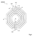
- Figure 6 shows a structure inductors L15, L16 according to the present invention
- the track conductive 70 has a substantially octagonal shape between a first end 72, on the external side of the winding and a second end 74, on the internal side of the winding.
- a first terminal A15 of the inductor L15 is constituted by the first end 72 of runway 70.
- a second terminal B15 of inductor L15 is connected to the second end 74 of the track 70 via a conductive segment 76.
- Inductance L16 is formed by the part of the conductive track 70 located between the end 74 and a point J3.
- a second conductive segment 78 connects point J3 to a first terminal A16 of inductance L16.
- the second terminal of the L16 inductor is made up via terminal B15.
- the second inductance inductance structures according to the present invention is formed by the part of the conductive track located between the second terminal of the first inductor and a predetermined point.
- the skilled person will easily adapt the present invention in case the second inductor is formed by the part of the conductive track located between the first terminal and said predetermined point.
Landscapes
- Engineering & Computer Science (AREA)
- Power Engineering (AREA)
- Microelectronics & Electronic Packaging (AREA)
- Coils Or Transformers For Communication (AREA)
Abstract
Description
Claims (8)
- Circuit intégré comprenant une structure d'inductances sur un substrat semiconducteur, destinée à fonctionner à des fréquences supérieures à plusieurs centaines de MHz, comportant une première inductance formée par une piste conductrice (38) et présentant des première (A5) et deuxième (B5) bornes reliées respectivement à chacune des deux extrémités (40, 42) de la piste conductrice, caractérisé en ce qu'il comprendune deuxième inductance formée par la piste conductrice entre la deuxième borne et un point intermédiaire quelconque (J) de la piste conductrice relié à une troisième borne (A6), lesdites deuxième et troisième bornes constituant les deux bornes de la deuxième inductance, etdes moyens pour mettre la troisième borne à haute impédance quand la première inductance est utilisée.
- Circuit selon la revendication 1, dans lequel la piste conductrice (38) est formée de segments rectilignes.
- Circuit selon la revendication 2, dans lequel la piste conductrice (70) est sensiblement de forme octogonale.
- Circuit selon la revendication 1, dans lequel ledit point intermédiaire est relié à la troisième borne par l'intermédiaire d'un segment conducteur rectiligne (44).
- Circuit selon la revendication 4, dans lequel ledit segment conducteur (44) est sensiblement perpendiculaire à la piste conductrice.
- Circuit selon l'une quelconque des revendications 1 à 5, comprenant au moins une deuxième structure d'inductances symétrique de la première structure et formée des mêmes éléments, dans lequel les pistes conductrices (50 ; 60) des première et deuxième structures sont imbriquées l'une dans l'autre de sorte que les deux pistes conductrices sont de même longueur, et dans lequel les distances de chacun des points intermédiaires (J1 ; J2) de chacune des pistes conductrices (50 ; 60) des première et deuxième structures d'inductances à la deuxième extrémité desdites pistes conductrices sont égales.
- Circuit selon l'une quelconque des revendications 1 à 5, comprenant des première et deuxième chaínes de traitement (T1, T2), la première chaíne (T1) comportant un premier mélangeur (16) propre à utiliser une première fréquence (f1) et la deuxième chaíne (T2) comportant un deuxième mélangeur (22) propre à utiliser une deuxième fréquence (f2), la première borne de la première inductance étant reliée au premier mélangeur, la deuxième borne de la première inductance étant reliée à une masse du circuit, et la troisième borne de la deuxième inductance étant reliée au deuxième mélangeur.
- Circuit selon la revendication 7, comportant une deuxième structure d'inductances identique à la première structure, la première borne de la première inductance de la deuxième structure étant reliée au premier mélangeur, la deuxième borne de la première inductance de la deuxième structure étant reliée à la masse du circuit, et la troisième borne de la deuxième inductance de la deuxième structure étant reliée au deuxième mélangeur.
Applications Claiming Priority (2)
| Application Number | Priority Date | Filing Date | Title |
|---|---|---|---|
| FR0010066 | 2000-07-31 | ||
| FR0010066A FR2812445B1 (fr) | 2000-07-31 | 2000-07-31 | Structure integree d'inductances a valeurs partagees sur un substrat semiconducteur |
Publications (2)
| Publication Number | Publication Date |
|---|---|
| EP1178500A1 true EP1178500A1 (fr) | 2002-02-06 |
| EP1178500B1 EP1178500B1 (fr) | 2009-09-09 |
Family
ID=8853132
Family Applications (1)
| Application Number | Title | Priority Date | Filing Date |
|---|---|---|---|
| EP01410093A Expired - Lifetime EP1178500B1 (fr) | 2000-07-31 | 2001-07-23 | Structure intégrée d'inductances à valeurs partagées sur un substrat semiconducteur |
Country Status (4)
| Country | Link |
|---|---|
| US (2) | US6993313B2 (fr) |
| EP (1) | EP1178500B1 (fr) |
| DE (1) | DE60139841D1 (fr) |
| FR (1) | FR2812445B1 (fr) |
Cited By (1)
| Publication number | Priority date | Publication date | Assignee | Title |
|---|---|---|---|---|
| DE10214068A1 (de) * | 2002-03-28 | 2003-10-23 | Advanced Micro Devices Inc | ESD-Schutzschaltung für Radiofrequenz- Ein/Ausgangsanschlüsse in einer integrierten Schaltung |
Families Citing this family (13)
| Publication number | Priority date | Publication date | Assignee | Title |
|---|---|---|---|---|
| FR2812445B1 (fr) * | 2000-07-31 | 2002-11-29 | St Microelectronics Sa | Structure integree d'inductances a valeurs partagees sur un substrat semiconducteur |
| US7787838B2 (en) * | 2002-04-30 | 2010-08-31 | 4472314 Canada Inc. | Integrated circuit, and an arrangement and method for interconnecting components of an integrated circuit |
| AU2003244928A1 (en) * | 2002-07-23 | 2004-02-09 | Koninklijke Philips Electronics N.V. | Multi-tap coil |
| US7123122B2 (en) * | 2003-04-18 | 2006-10-17 | Medtronic, Inc. | Center tapped chip inductor |
| FI20055402A0 (fi) * | 2005-07-11 | 2005-07-11 | Nokia Corp | Induktorilaite monikaistaista radiotaajuista toimintaa varten |
| US7761078B2 (en) * | 2006-07-28 | 2010-07-20 | Qualcomm Incorporated | Dual inductor circuit for multi-band wireless communication device |
| US8219060B2 (en) * | 2006-07-28 | 2012-07-10 | Qualcomm Incorporated | Dual inductor circuit for multi-band wireless communication device |
| US7688160B2 (en) * | 2007-04-12 | 2010-03-30 | Stats Chippac, Ltd. | Compact coils for high performance filters |
| JP5114793B2 (ja) * | 2009-03-03 | 2013-01-09 | 旭化成エレクトロニクス株式会社 | 可変インダクタ及び電圧制御発振器 |
| TWI410987B (zh) * | 2011-05-26 | 2013-10-01 | 矽品精密工業股份有限公司 | 非對稱式差動電感 |
| US9281681B2 (en) * | 2012-11-21 | 2016-03-08 | Taiwan Semiconductor Manufacturing Co., Ltd. | ESD protection circuits and methods |
| ES2637119T3 (es) * | 2013-10-16 | 2017-10-10 | Telefonaktiebolaget Lm Ericsson (Publ) | Disposición, transceptor, procedimiento y programa informático de inductor sintonizable |
| US10680552B2 (en) * | 2017-09-29 | 2020-06-09 | Intel IP Corporation | On-chip oscillators including shared inductor |
Citations (3)
| Publication number | Priority date | Publication date | Assignee | Title |
|---|---|---|---|---|
| DE3941323A1 (de) * | 1988-12-14 | 1990-06-21 | Fraunhofer Ges Forschung | Halbleiterelement mit einer integrierten induktivitaet |
| US5892425A (en) * | 1997-04-10 | 1999-04-06 | Virginia Tech Intellectual Properties, Inc. | Interwound center-tapped spiral inductor |
| EP0940826A2 (fr) * | 1998-03-06 | 1999-09-08 | International Business Machines Corporation | Inducteur pour utilisation dans des oscillateurs électroniques |
Family Cites Families (17)
| Publication number | Priority date | Publication date | Assignee | Title |
|---|---|---|---|---|
| DE1952604A1 (de) * | 1969-10-18 | 1971-04-29 | Bosch Gmbh Robert | Schaltungsanordnung zur Abgabe von Impulsen |
| US3727078A (en) * | 1972-03-30 | 1973-04-10 | Nat Semiconductor Corp | Integrated circuit balanced mixer apparatus |
| US4449245A (en) * | 1982-03-22 | 1984-05-15 | Motorola Inc. | High gain balanced mixer |
| FR2561835B1 (fr) * | 1984-03-26 | 1986-07-18 | Adret Electronique | Melangeur doublement equilibre a diodes comportant un modulateur en anneau dont chaque branche comporte une diode rapide classique en serie avec au moins une diode du genre " varactor " |
| US4816784A (en) * | 1988-01-19 | 1989-03-28 | Northern Telecom Limited | Balanced planar transformers |
| JPH03160803A (ja) * | 1989-11-20 | 1991-07-10 | Pioneer Electron Corp | バランスドミキサー回路 |
| US5006811A (en) * | 1990-01-31 | 1991-04-09 | Triquint Semiconductor, Inc. | Dual quadrature frequency converter |
| FI93679C (fi) * | 1991-10-23 | 1995-05-10 | Nokia Mobile Phones Ltd | Taajuusselektiivinen mikroliuskamuuntaja sekä diodisekoitin |
| US5477204A (en) * | 1994-07-05 | 1995-12-19 | Motorola, Inc. | Radio frequency transformer |
| JPH0936312A (ja) * | 1995-07-18 | 1997-02-07 | Nec Corp | インダクタンス素子およびその製造方法 |
| US5774801A (en) * | 1995-08-23 | 1998-06-30 | Ericsson Inc. | High dynamic range mixer having low conversion loss, low local oscillator input power, and high dynamic range and a method for designing the same |
| US6026286A (en) * | 1995-08-24 | 2000-02-15 | Nortel Networks Corporation | RF amplifier, RF mixer and RF receiver |
| US5917386A (en) * | 1997-03-12 | 1999-06-29 | Zenith Electronics Corporation | Printed circuit transformer hybrids for RF mixers |
| AU2147900A (en) * | 1998-11-12 | 2000-05-29 | Broadcom Corporation | Fully integrated tuner architecture |
| US6885275B1 (en) * | 1998-11-12 | 2005-04-26 | Broadcom Corporation | Multi-track integrated spiral inductor |
| US7072636B2 (en) * | 1999-03-25 | 2006-07-04 | Zenith Electronics Corporation | Printed circuit doubly balanced mixer for upconverter |
| FR2812445B1 (fr) * | 2000-07-31 | 2002-11-29 | St Microelectronics Sa | Structure integree d'inductances a valeurs partagees sur un substrat semiconducteur |
-
2000
- 2000-07-31 FR FR0010066A patent/FR2812445B1/fr not_active Expired - Fee Related
-
2001
- 2001-07-23 EP EP01410093A patent/EP1178500B1/fr not_active Expired - Lifetime
- 2001-07-23 DE DE60139841T patent/DE60139841D1/de not_active Expired - Lifetime
- 2001-07-30 US US09/918,792 patent/US6993313B2/en not_active Expired - Lifetime
-
2005
- 2005-12-06 US US11/294,802 patent/US7751793B2/en not_active Expired - Fee Related
Patent Citations (3)
| Publication number | Priority date | Publication date | Assignee | Title |
|---|---|---|---|---|
| DE3941323A1 (de) * | 1988-12-14 | 1990-06-21 | Fraunhofer Ges Forschung | Halbleiterelement mit einer integrierten induktivitaet |
| US5892425A (en) * | 1997-04-10 | 1999-04-06 | Virginia Tech Intellectual Properties, Inc. | Interwound center-tapped spiral inductor |
| EP0940826A2 (fr) * | 1998-03-06 | 1999-09-08 | International Business Machines Corporation | Inducteur pour utilisation dans des oscillateurs électroniques |
Non-Patent Citations (1)
| Title |
|---|
| CHEUNG D T S ET AL: "MONOLITHIC TRANSFORMERS FOR SILICON RF IC DESIGN", MELECON CONFERENCES,US,NEW YORK, NY: IEEE, 18 May 1998 (1998-05-18), pages 105 - 108, XP000802034, ISBN: 0-7803-3880-4 * |
Cited By (3)
| Publication number | Priority date | Publication date | Assignee | Title |
|---|---|---|---|---|
| DE10214068A1 (de) * | 2002-03-28 | 2003-10-23 | Advanced Micro Devices Inc | ESD-Schutzschaltung für Radiofrequenz- Ein/Ausgangsanschlüsse in einer integrierten Schaltung |
| US7224949B2 (en) | 2002-03-28 | 2007-05-29 | Advanced Micro Devices, Inc. | ESD protection circuit for radio frequency input/output terminals in an integrated circuit |
| DE10214068B4 (de) * | 2002-03-28 | 2009-02-19 | Advanced Micro Devices, Inc., Sunnyvale | ESD-Schutzschaltung für Radiofrequenz-Ausgangsanschlüsse in einer integrierten Schaltung |
Also Published As
| Publication number | Publication date |
|---|---|
| US20060084401A1 (en) | 2006-04-20 |
| FR2812445B1 (fr) | 2002-11-29 |
| US20020013134A1 (en) | 2002-01-31 |
| DE60139841D1 (de) | 2009-10-22 |
| FR2812445A1 (fr) | 2002-02-01 |
| US6993313B2 (en) | 2006-01-31 |
| US7751793B2 (en) | 2010-07-06 |
| EP1178500B1 (fr) | 2009-09-09 |
Similar Documents
| Publication | Publication Date | Title |
|---|---|---|
| EP1178500B1 (fr) | Structure intégrée d'inductances à valeurs partagées sur un substrat semiconducteur | |
| EP2246931B1 (fr) | Filtre de mode commun à inductances couplées | |
| EP1863116B1 (fr) | Coupleur directif large bande | |
| EP1097509B1 (fr) | Modulateur vectoriel | |
| EP1427053A1 (fr) | Coupleur directif | |
| EP0013222A1 (fr) | Déphaseur hyperfréquence à diodes et antenne à balayage électronique comportant un tel déphaseur | |
| EP0627765A1 (fr) | Dispositif semiconducteur incluant un élément semiconducteur du type "FLIP-CHIP" | |
| EP1601101A1 (fr) | Transformateur à changement de mode et filtre passe-bas | |
| FR2877163A1 (fr) | Reglage du rapport d'impedances d'un balun | |
| FR2984603A1 (fr) | Circuit integre comprenant un transformateur integre de type "balun" a plusieurs voies d'entree et de sortie. | |
| EP0300893B1 (fr) | Dispositif de retard hyperfréquence | |
| EP1445801A1 (fr) | Inductance intégrée et circuit électronique l'incorporant | |
| FR2894062A1 (fr) | Balun a rapport d'impedances 1/4 | |
| EP1429458A2 (fr) | Transformateur à changement de mode sélectif en fréquences | |
| EP0905852A1 (fr) | Circuit de protection associable à un filtre | |
| FR2826723A1 (fr) | Systeme de mesure capacitif | |
| FR2862158A1 (fr) | Balun distribue a rapport d'impedance non unitaire | |
| FR2859584A1 (fr) | Balun distribue de type marchand | |
| FR2801969A1 (fr) | Capteur analogique de decalage angulaire sans contact | |
| FR2788129A1 (fr) | Detecteur bolometrique a antenne | |
| FR2549314A1 (fr) | Quadrupole d'adaptation, independante de la frequence de fonctionnement, d'une reactance, et amplificateur a ondes progressives utilisant un tel quadrupole | |
| EP1521363A1 (fr) | Coupleur intégré | |
| FR3077432A1 (fr) | Filtre de mode commun | |
| EP0015168A1 (fr) | Magnétomètre à ondes magnétostatiques | |
| EP1580837B1 (fr) | Dispositif semi-conducteur à antenne et écran collecteur |
Legal Events
| Date | Code | Title | Description |
|---|---|---|---|
| PUAI | Public reference made under article 153(3) epc to a published international application that has entered the european phase |
Free format text: ORIGINAL CODE: 0009012 |
|
| AK | Designated contracting states |
Kind code of ref document: A1 Designated state(s): AT BE CH CY DE DK ES FI FR GB GR IE IT LI LU MC NL PT SE TR Kind code of ref document: A1 Designated state(s): DE FR GB |
|
| AX | Request for extension of the european patent |
Free format text: AL;LT;LV;MK;RO;SI |
|
| 17P | Request for examination filed |
Effective date: 20020722 |
|
| AKX | Designation fees paid |
Free format text: DE FR GB |
|
| 17Q | First examination report despatched |
Effective date: 20080526 |
|
| GRAP | Despatch of communication of intention to grant a patent |
Free format text: ORIGINAL CODE: EPIDOSNIGR1 |
|
| GRAS | Grant fee paid |
Free format text: ORIGINAL CODE: EPIDOSNIGR3 |
|
| GRAA | (expected) grant |
Free format text: ORIGINAL CODE: 0009210 |
|
| AK | Designated contracting states |
Kind code of ref document: B1 Designated state(s): DE FR GB |
|
| REG | Reference to a national code |
Ref country code: GB Ref legal event code: FG4D Free format text: NOT ENGLISH |
|
| REF | Corresponds to: |
Ref document number: 60139841 Country of ref document: DE Date of ref document: 20091022 Kind code of ref document: P |
|
| PLBE | No opposition filed within time limit |
Free format text: ORIGINAL CODE: 0009261 |
|
| STAA | Information on the status of an ep patent application or granted ep patent |
Free format text: STATUS: NO OPPOSITION FILED WITHIN TIME LIMIT |
|
| 26N | No opposition filed |
Effective date: 20100610 |
|
| PGFP | Annual fee paid to national office [announced via postgrant information from national office to epo] |
Ref country code: GB Payment date: 20120629 Year of fee payment: 12 |
|
| PGFP | Annual fee paid to national office [announced via postgrant information from national office to epo] |
Ref country code: DE Payment date: 20120625 Year of fee payment: 12 Ref country code: FR Payment date: 20120806 Year of fee payment: 12 |
|
| GBPC | Gb: european patent ceased through non-payment of renewal fee |
Effective date: 20130723 |
|
| REG | Reference to a national code |
Ref country code: DE Ref legal event code: R119 Ref document number: 60139841 Country of ref document: DE Effective date: 20140201 |
|
| REG | Reference to a national code |
Ref country code: FR Ref legal event code: ST Effective date: 20140331 |
|
| PG25 | Lapsed in a contracting state [announced via postgrant information from national office to epo] |
Ref country code: DE Free format text: LAPSE BECAUSE OF NON-PAYMENT OF DUE FEES Effective date: 20140201 Ref country code: GB Free format text: LAPSE BECAUSE OF NON-PAYMENT OF DUE FEES Effective date: 20130723 |
|
| PG25 | Lapsed in a contracting state [announced via postgrant information from national office to epo] |
Ref country code: FR Free format text: LAPSE BECAUSE OF NON-PAYMENT OF DUE FEES Effective date: 20130731 |