EP1178493A1 - Ceramic capacitor electrode-forming paste - Google Patents
Ceramic capacitor electrode-forming paste Download PDFInfo
- Publication number
- EP1178493A1 EP1178493A1 EP00987696A EP00987696A EP1178493A1 EP 1178493 A1 EP1178493 A1 EP 1178493A1 EP 00987696 A EP00987696 A EP 00987696A EP 00987696 A EP00987696 A EP 00987696A EP 1178493 A1 EP1178493 A1 EP 1178493A1
- Authority
- EP
- European Patent Office
- Prior art keywords
- weight
- powder
- electrode
- paste
- particle powder
- Prior art date
- Legal status (The legal status is an assumption and is not a legal conclusion. Google has not performed a legal analysis and makes no representation as to the accuracy of the status listed.)
- Granted
Links
Images



Classifications
-
- H—ELECTRICITY
- H01—ELECTRIC ELEMENTS
- H01G—CAPACITORS; CAPACITORS, RECTIFIERS, DETECTORS, SWITCHING DEVICES, LIGHT-SENSITIVE OR TEMPERATURE-SENSITIVE DEVICES OF THE ELECTROLYTIC TYPE
- H01G4/00—Fixed capacitors; Processes of their manufacture
- H01G4/002—Details
- H01G4/005—Electrodes
- H01G4/008—Selection of materials
- H01G4/0085—Fried electrodes
Definitions
- the present invention relates to a paste for formation of ceramic capacitor electrode.
- Capacitors are an electronic part in which a dielectric layer placed between two electrode layers is allowed to have an electrostatic capacity. As shown in Fig. 1, a capacitor 1 has a structure in which two electrode layers 3 are placed on the upper and lower surfaces of a dielectric layer 2. In recent years, ceramic capacitors using a ceramic dielectric made of barium titanate (BaTiO 3 ) or the like have been used in order to impart heat resistance, corrosion resistance, etc. to a capacitor.
- barium titanate BaTiO 3
- capacitors have become smaller as well.
- the electrode layer a film formed with a paste and moreover, in order to achieve a small size and yet a large capacity, employ a laminated structure such as shown in Fig. 2.
- conventional ceramic capacitors have, in some cases, through holes in the electrode layer. Owing to the difference in sizes of these through holes, the effective electrode area of capacitor (which determines the capacity of capacitor) varies between capacitors. As a result, the capacity of capacitor differs greatly between capacitors and there has been an inconvenience of low yield of capacitor properties.
- the present invention has been made in view of such a situation.
- the object of the present invention is to provide a paste for formation of ceramic capacitor electrode, capable of forming an electrode layer of ceramic capacitor which hardly peels from the dielectric layer of the capacitor and giving an increased capacitor yield in production of ceramic capacitor.
- a paste for formation of ceramic capacitor electrode composed of 10 to 14% by weight of an organic vehicle and 86 to 90% by weight of a platinum powder, wherein the platinum powder contains, in 100% by weight of the powder, 54 to 60% by weight of a spherical particle powder, 36 to 40% by weight of a flaky particle powder and 0 to 10% by weight of an indefinite particle powder.
- the paste for formation of electrode according to the present invention is composed of 10 to 14% by weight of an organic vehicle and 86 to 90% by weight of a platinum powder, wherein the platinum powder contains, in 100% by weight of the powder, 54 to 60% by weight of a spherical particle powder, 36 to 40% by weight of a flaky particle powder and 0 to 10% by weight of an indefinite particle powder.
- the reason for specifying the content of the platinum powder in the paste for formation of electrode, at 86 to 90% by weight, is that when the content is less than 86% by weight, a reduction in film density takes place and, when the content is more than 90% by weight, deterioration in printability takes place. More preferably, the content of the platinum powder is 88 to 90% by weight and the content of the organic vehicle is 10 to 12% by weight.
- the reason for specifying, in 100% by weight of the platinum powder, the proportion of the spherical particle powder at 54 to 60% by weight, the proportion of the flaky particle powder at 36 to 40% by weight and the proportion of the indefinite particle powder at 0 to 10% by weight, is to allow the formed electrode layer film of capacitor to have a density of 80% or more, a surface roughness (Ra) of 0.4 to 0.6 ⁇ m and an adhesion strength of 2 kg or more.
- film density is a concept indicating the compactness of electrode film, and refers to a value [(total electrode area - hole area)/(total electrode area)] obtained by taking photographs of an electrode surface at several different places using an electron microscope or a metallurgical microscope and calculating the hole area and the total electrode area. Therefore, a larger film density indicates that the through holes generated in the film formed on an electrode layer are smaller in size and number.
- the film density is controlled, whereby the through holes are made small in size and number and the dispersion of capacitor capacity is made small. Also, the deterioration of capacitor properties can be suppressed.
- the reason why the film density becomes 80% or more by specifying the proportions of the platinum powders of different particle shapes in the above ranges is that mixing of three kinds of powders different in particle shape in a good balance allows for a higher packing density of powder in paste and a smaller contraction during firing.
- the adhesivity of the film to the dielectric layer can be enhanced and the peeling of the electrode layer from the dielectric layer can be made substantially nil.
- the adhesivity of the film is increased with no reduction in film density; it is because in the laminated capacitor structure, the platinum adheres to the base material by a chemical bonding force brought about by diffusion of platinum into base material and also by a physical bonding force brought about by an anchor effect having a close relation with the surface roughness.
- surface roughness (Ra) is a value obtained by JIS B 0601.
- Adhesion strength is a concept indicating an adhesivity between base material and conductor, and refers to a tensile strength obtained when an L-shaped lead wire of 0.6 mm in diameter consisting of a tin-coated soft copper wire is attached to a 2 mm x 2 mm conductor pattern by soldering and is pulled vertically at a tensile speed of 20 mm/sec.
- the surface roughness (Ra) is controlled at 0.4 to 0.6 ⁇ m; the reason therefor is that the flaky particle powder of large particle diameters constitutes the skeleton of electrode layer, the spherical particle powder and the indefinite particle powder both having small particle diameters fill the gaps present between the skeleton, and thereby the surface roughness after firing is stabilized.
- the reason why the adhesion strength becomes 2 kg or more, is that the spherical particle powder and the indefinite particle powder both small in particle diameter are rich in surface activity and therefore can easily diffuse into the base material.
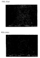
- Figs. 3(a) and 3(b), Figs. 4(a) and 4(b) and Figs. 5(a) and 5(b) show photographs of a spherical particle powder, a flaky particle powder and an indefinite particle powder, respectively, by secondary electron microscope observation.
- the spherical particle power is a powder of substantially spherical particles having diameters of submicron order;
- the flaky particle powder is a powder of flat particles whose major diameters are a micron order;
- the indefinite particle diameter is a powder whose primary particles have diameters of ⁇ order, and large particles seen at some places are secondary particles formed by agglomeration of primary particles.
- the proportions of the platinum powders of different particle shapes constituting the paste are specified in given ranges; thereby, the electrode layer film made from the paste has a controlled density, a controlled surface roughness (Ra) and a controlled adhesion strength; this makes small the dispersion of capacitor capacity and prevents the deterioration of capacitor properties.
- the proportions of the spherical particle powder, the flaky particle powder and the indefinite particle powder are more preferably 57 to 60% by weight, 38 to 40% by weight and 0 to 5% by weight, respectively.
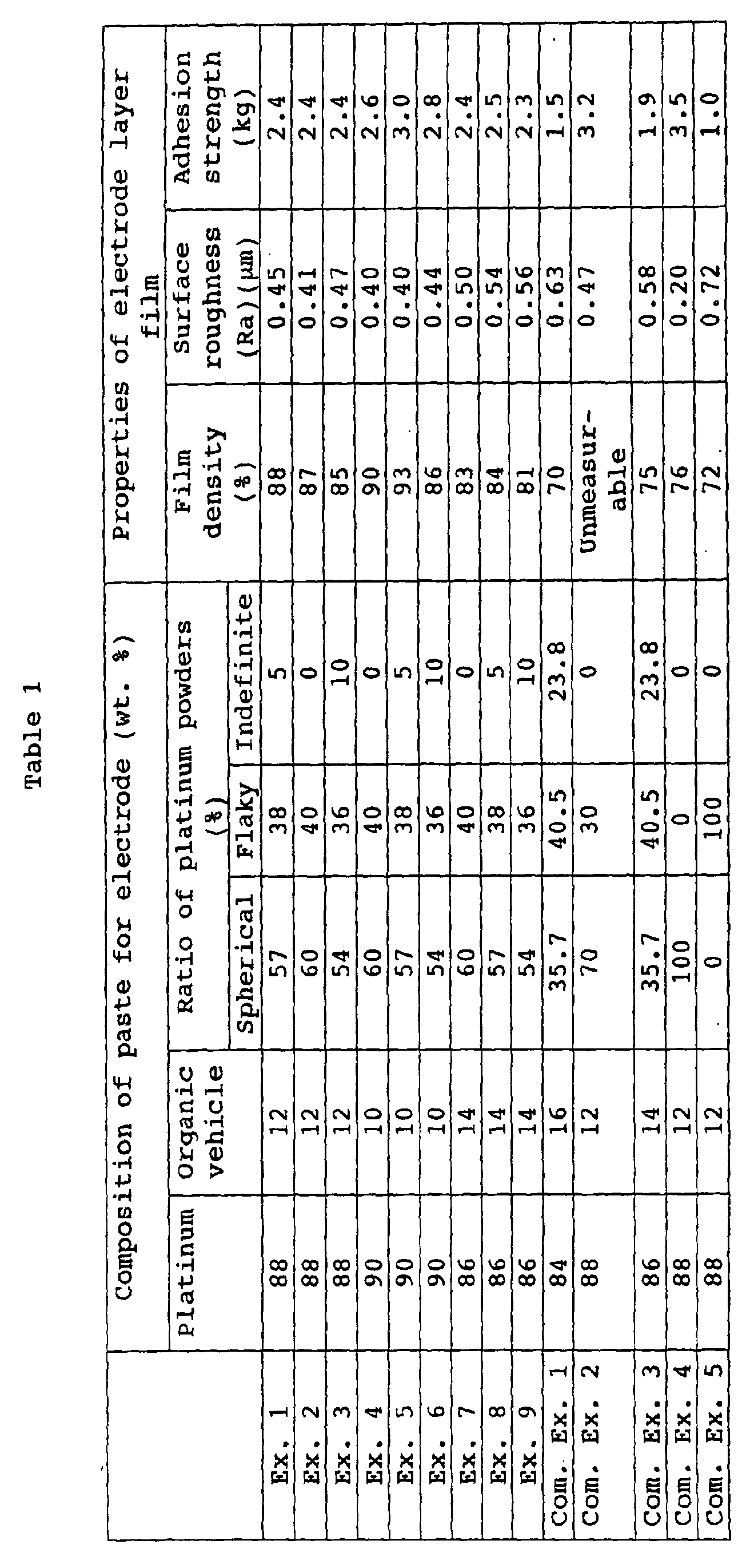
- the lower electrode film of the capacitor had a density of 88%, a surface roughness (Ra) of 0.45 ⁇ m and an adhesion strength of 2.4 kg.
- the dielectric layer was constituted by lead zirconate titanate and had a thickness of 20 ⁇ m.
- the electrode layers had a thickness of 4 ⁇ m.
- a ceramic capacitor was produced in the same manner as in Example 1.
- the lower electrode film of the ceramic capacitor was allowed to have a density, a surface roughness (Ra) and an adhesion strength, all shown in Table 1.
- Example 2 There were compounded 16% by weight of an organic vehicle and 84% by weight of the same platinum powder as used in Example 1 (which consisted of 35.7% by weight of a spherical particle powder, 40.5% by weight of a flaky particle powder and 23.8% by weight of an indefinite particle powder), to obtain a paste for electrode. Using the paste was produced the same ceramic capacitor as in Example 1.
- the lower electrode film of the capacitor had a density of 70%, a surface roughness (Ra) of 0.63 ⁇ m and an adhesion strength of 1.5 kg.
- a ceramic capacitor was produced in the same manner as in Example 1.
- the lower electrode film of the ceramic capacitor was allowed to have a density, a surface roughness (Ra) and an adhesion strength, all shown in Table 1.
- the proportions of the platinum powders of different particle shapes contained in the paste are specified in given ranges. Therefore, in the ceramic capacitor produced using the paste, the electrode layer film has a density, a surface roughness (Ra) and an adhesion strength all specified at given values; the adhesivity of the electrode layer to the dielectric layer can be improved; and the through holes generated in the electrode layer can be made small.
Landscapes
- Engineering & Computer Science (AREA)
- Power Engineering (AREA)
- Chemical & Material Sciences (AREA)
- Materials Engineering (AREA)
- Manufacturing & Machinery (AREA)
- Microelectronics & Electronic Packaging (AREA)
- Conductive Materials (AREA)
- Fixed Capacitors And Capacitor Manufacturing Machines (AREA)
- Ceramic Capacitors (AREA)
Abstract
Description

Claims (4)
- A paste for formation of ceramic capacitor electrode, composed of 10 to 14% by weight of an organic vehicle and 86 to 90% by weight of a platinum powder, wherein the platinum powder contains, in 100% by weight of the powder, 54 to 60% by weight of a spherical particle powder, 36 to 40% by weight of a flaky particle powder and 0 to 10% by weight of an indefinite particle powder.
- A paste for formation of electrode according to Claim 1, composed of 10 to 12% by weight of an organic vehicle and 88 to 90% by weight of a platinum powder.
- A paste for formation of electrode according to Claim 1, wherein the platinum powder contains, in 100% by weight of the powder, 57 to 60% by weight of a spherical particle powder, 38 to 40% by weight of a flaky particle powder and 0 to 5% by weight of an indefinite particle powder.
- A paste for formation of electrode according to Claim 1, capable of forming an electrode layer film of ceramic capacitor having a density of 80% or more, a surface roughness (Ra) of 0.4 to 0.6 µm and an adhesion strength of 2 kg or more.
Applications Claiming Priority (3)
| Application Number | Priority Date | Filing Date | Title |
|---|---|---|---|
| JP36852599 | 1999-12-24 | ||
| JP36852599A JP3908426B2 (en) | 1999-12-24 | 1999-12-24 | Ceramic capacitor electrode forming paste |
| PCT/JP2000/009117 WO2001048762A1 (en) | 1999-12-24 | 2000-12-22 | Ceramic capacitor electrode-forming paste |
Publications (3)
| Publication Number | Publication Date |
|---|---|
| EP1178493A1 true EP1178493A1 (en) | 2002-02-06 |
| EP1178493A4 EP1178493A4 (en) | 2005-06-15 |
| EP1178493B1 EP1178493B1 (en) | 2007-02-14 |
Family
ID=18492058
Family Applications (1)
| Application Number | Title | Priority Date | Filing Date |
|---|---|---|---|
| EP00987696A Expired - Lifetime EP1178493B1 (en) | 1999-12-24 | 2000-12-22 | Ceramic capacitor electrode-forming paste |
Country Status (5)
| Country | Link |
|---|---|
| US (1) | US6565774B2 (en) |
| EP (1) | EP1178493B1 (en) |
| JP (1) | JP3908426B2 (en) |
| DE (1) | DE60033386T2 (en) |
| WO (1) | WO2001048762A1 (en) |
Families Citing this family (8)
| Publication number | Priority date | Publication date | Assignee | Title |
|---|---|---|---|---|
| US6338809B1 (en) * | 1997-02-24 | 2002-01-15 | Superior Micropowders Llc | Aerosol method and apparatus, particulate products, and electronic devices made therefrom |
| EP1007308B1 (en) * | 1997-02-24 | 2003-11-12 | Superior Micropowders LLC | Aerosol method and apparatus, particulate products, and electronic devices made therefrom |
| US20050097987A1 (en) * | 1998-02-24 | 2005-05-12 | Cabot Corporation | Coated copper-containing powders, methods and apparatus for producing such powders, and copper-containing devices fabricated from same |
| US7615939B2 (en) * | 2003-03-17 | 2009-11-10 | C&D Zodiac, Inc. | Spectrally calibratable multi-element RGB LED light source |
| JP2007242880A (en) * | 2006-03-08 | 2007-09-20 | Tdk Corp | Deposition method |
| JP4983102B2 (en) * | 2006-06-06 | 2012-07-25 | Tdk株式会社 | Dielectric element |
| CA2676218C (en) * | 2007-01-22 | 2016-01-19 | University Of Maryland | High temperature solder materials |
| CN111028981A (en) * | 2019-12-27 | 2020-04-17 | 有研亿金新材料有限公司 | A kind of platinum electrode slurry and its preparation method and application |
Family Cites Families (15)
| Publication number | Priority date | Publication date | Assignee | Title |
|---|---|---|---|---|
| GB2133623A (en) * | 1982-12-20 | 1984-07-25 | Engelhard Ind Ltd | Ceramic multilayer electrical capacitors |
| JPH0198674A (en) * | 1987-10-09 | 1989-04-17 | Daido Steel Co Ltd | conductive composition |
| JPH01315903A (en) * | 1988-06-14 | 1989-12-20 | Tdk Corp | Electricaly conductive paste and chip parts |
| JPH0817141B2 (en) * | 1988-07-28 | 1996-02-21 | 昭栄化学工業株式会社 | Conductive composition for ceramic capacitor terminal electrodes |
| JPH0834168B2 (en) | 1988-10-19 | 1996-03-29 | 昭栄化学工業株式会社 | Conductive composition for ceramic capacitor terminal electrodes |
| US4954926A (en) * | 1989-07-28 | 1990-09-04 | E. I. Du Pont De Nemours And Company | Thick film conductor composition |
| JPH0777086B2 (en) * | 1990-09-20 | 1995-08-16 | 住友金属鉱山株式会社 | Conductive resin paste |
| JPH05334911A (en) * | 1992-06-02 | 1993-12-17 | Ishifuku Metal Ind Co Ltd | Platinum conductive paste for baking and method for producing the same |
| JPH0878267A (en) * | 1994-09-08 | 1996-03-22 | Murata Mfg Co Ltd | Internal electrode paste and multilayer ceramic capacitor using the same |
| JPH0896623A (en) * | 1994-09-28 | 1996-04-12 | Murata Mfg Co Ltd | Conductive paste |
| JPH08115612A (en) * | 1994-10-13 | 1996-05-07 | Murata Mfg Co Ltd | Conductive paste |
| JP3063549B2 (en) * | 1994-11-25 | 2000-07-12 | 株式会社村田製作所 | Conductive paste |
| JPH1092226A (en) * | 1996-09-11 | 1998-04-10 | Murata Mfg Co Ltd | Conductive composition |
| JP4012960B2 (en) * | 1996-09-12 | 2007-11-28 | Dowaエレクトロニクス株式会社 | Silver powder manufacturing method |
| US6108210A (en) * | 1998-04-24 | 2000-08-22 | Amerasia International Technology, Inc. | Flip chip devices with flexible conductive adhesive |
-
1999
- 1999-12-24 JP JP36852599A patent/JP3908426B2/en not_active Expired - Fee Related
-
2000
- 2000-12-22 DE DE60033386T patent/DE60033386T2/en not_active Expired - Lifetime
- 2000-12-22 WO PCT/JP2000/009117 patent/WO2001048762A1/en not_active Ceased
- 2000-12-22 EP EP00987696A patent/EP1178493B1/en not_active Expired - Lifetime
- 2000-12-22 US US09/889,194 patent/US6565774B2/en not_active Expired - Fee Related
Also Published As
| Publication number | Publication date |
|---|---|
| EP1178493A4 (en) | 2005-06-15 |
| US6565774B2 (en) | 2003-05-20 |
| DE60033386D1 (en) | 2007-03-29 |
| WO2001048762A1 (en) | 2001-07-05 |
| US20030033956A1 (en) | 2003-02-20 |
| DE60033386T2 (en) | 2007-11-08 |
| EP1178493B1 (en) | 2007-02-14 |
| JP2001184942A (en) | 2001-07-06 |
| JP3908426B2 (en) | 2007-04-25 |
Similar Documents
| Publication | Publication Date | Title |
|---|---|---|
| JP7379899B2 (en) | ceramic electronic components | |
| EP2713378B1 (en) | Laminated chip electronic component, board for mounting the same, and packing unit thereof | |
| US8867190B2 (en) | Multilayer ceramic electronic component having an average surface roughness to provide adhesion strength between a dielectric layer and inner electrode and fabrication method thereof | |
| JP3527899B2 (en) | Laminated electronic component and method of manufacturing the same | |
| EP1553605A2 (en) | Multilayer ceramic capacitor and its production method | |
| US11657974B2 (en) | Multilayer ceramic capacitor | |
| US20250095918A1 (en) | Multilayer ceramic capacitor and mounting structure of multilayer ceramic capacitor | |
| KR20180057001A (en) | Conductive powder for inner electrode and capacitor | |
| JP4688326B2 (en) | Ceramic laminate and manufacturing method thereof | |
| US6565774B2 (en) | Paste for formation of ceramic capacitor electrode | |
| JP3736802B2 (en) | Conductive composition and ceramic electronic component | |
| KR20020004881A (en) | Conductive paste and laminated ceramic electronic component using the same | |
| JP2002299145A (en) | Ceramic laminate and method for producing the same | |
| JP7565949B2 (en) | Electrolytic capacitor and method for manufacturing the same | |
| JP3692263B2 (en) | Multilayer ceramic capacitor | |
| JP3255011B2 (en) | Multilayer ceramic electronic components | |
| JP3596743B2 (en) | Manufacturing method of multilayer ceramic electronic component and multilayer ceramic electronic component | |
| JP3699617B2 (en) | Multilayer ceramic capacitor | |
| JP3391322B2 (en) | Multilayer capacitor and manufacturing method thereof | |
| JP4385726B2 (en) | Conductive paste and method for producing multilayer ceramic capacitor using the same | |
| CN1302496C (en) | Dielectric ceramic powder, ceramic raw piece, laminated ceramic capacitor and producing method thereof | |
| JP4529358B2 (en) | Ceramic green sheet | |
| EP0925860A2 (en) | Nickel ultrafine powder | |
| JP2022121214A (en) | Electrode material for aluminum electrolytic capacitor and manufacturing method thereof | |
| JP3534999B2 (en) | Conductive paste |
Legal Events
| Date | Code | Title | Description |
|---|---|---|---|
| PUAI | Public reference made under article 153(3) epc to a published international application that has entered the european phase |
Free format text: ORIGINAL CODE: 0009012 |
|
| 17P | Request for examination filed |
Effective date: 20010810 |
|
| AK | Designated contracting states |
Kind code of ref document: A1 Designated state(s): AT BE CH CY DE DK ES FI FR GB GR IE IT LI LU MC NL PT SE TR |
|
| RBV | Designated contracting states (corrected) |
Designated state(s): DE FR GB IT |
|
| A4 | Supplementary search report drawn up and despatched |
Effective date: 20050429 |
|
| GRAP | Despatch of communication of intention to grant a patent |
Free format text: ORIGINAL CODE: EPIDOSNIGR1 |
|
| RIC1 | Information provided on ipc code assigned before grant |
Ipc: H01B 1/00 20060101ALI20060721BHEP Ipc: H01G 4/252 20060101ALI20060721BHEP Ipc: H01B 1/22 20060101AFI20060721BHEP |
|
| GRAS | Grant fee paid |
Free format text: ORIGINAL CODE: EPIDOSNIGR3 |
|
| GRAA | (expected) grant |
Free format text: ORIGINAL CODE: 0009210 |
|
| AK | Designated contracting states |
Kind code of ref document: B1 Designated state(s): DE FR GB IT |
|
| REG | Reference to a national code |
Ref country code: GB Ref legal event code: FG4D |
|
| REF | Corresponds to: |
Ref document number: 60033386 Country of ref document: DE Date of ref document: 20070329 Kind code of ref document: P |
|
| ET | Fr: translation filed | ||
| PLBE | No opposition filed within time limit |
Free format text: ORIGINAL CODE: 0009261 |
|
| STAA | Information on the status of an ep patent application or granted ep patent |
Free format text: STATUS: NO OPPOSITION FILED WITHIN TIME LIMIT |
|
| 26N | No opposition filed |
Effective date: 20071115 |
|
| PGFP | Annual fee paid to national office [announced via postgrant information from national office to epo] |
Ref country code: GB Payment date: 20121128 Year of fee payment: 13 |
|
| PGFP | Annual fee paid to national office [announced via postgrant information from national office to epo] |
Ref country code: FR Payment date: 20121219 Year of fee payment: 13 |
|
| PGFP | Annual fee paid to national office [announced via postgrant information from national office to epo] |
Ref country code: DE Payment date: 20121221 Year of fee payment: 13 |
|
| PGFP | Annual fee paid to national office [announced via postgrant information from national office to epo] |
Ref country code: IT Payment date: 20131107 Year of fee payment: 14 |
|
| REG | Reference to a national code |
Ref country code: DE Ref legal event code: R119 Ref document number: 60033386 Country of ref document: DE |
|
| GBPC | Gb: european patent ceased through non-payment of renewal fee |
Effective date: 20131222 |
|
| REG | Reference to a national code |
Ref country code: DE Ref legal event code: R119 Ref document number: 60033386 Country of ref document: DE Effective date: 20140701 |
|
| REG | Reference to a national code |
Ref country code: FR Ref legal event code: ST Effective date: 20140829 |
|
| PG25 | Lapsed in a contracting state [announced via postgrant information from national office to epo] |
Ref country code: DE Free format text: LAPSE BECAUSE OF NON-PAYMENT OF DUE FEES Effective date: 20140701 |
|
| PG25 | Lapsed in a contracting state [announced via postgrant information from national office to epo] |
Ref country code: GB Free format text: LAPSE BECAUSE OF NON-PAYMENT OF DUE FEES Effective date: 20131222 Ref country code: FR Free format text: LAPSE BECAUSE OF NON-PAYMENT OF DUE FEES Effective date: 20131231 |
|
| PG25 | Lapsed in a contracting state [announced via postgrant information from national office to epo] |
Ref country code: IT Free format text: LAPSE BECAUSE OF NON-PAYMENT OF DUE FEES Effective date: 20141222 |