EP1178299A1 - Ultrafeine ritzprüfvorrichtung - Google Patents
Ultrafeine ritzprüfvorrichtung Download PDFInfo
- Publication number
- EP1178299A1 EP1178299A1 EP01902821A EP01902821A EP1178299A1 EP 1178299 A1 EP1178299 A1 EP 1178299A1 EP 01902821 A EP01902821 A EP 01902821A EP 01902821 A EP01902821 A EP 01902821A EP 1178299 A1 EP1178299 A1 EP 1178299A1
- Authority
- EP
- European Patent Office
- Prior art keywords
- lever
- indenter
- sample
- testing apparatus
- probe
- Prior art date
- Legal status (The legal status is an assumption and is not a legal conclusion. Google has not performed a legal analysis and makes no representation as to the accuracy of the status listed.)
- Withdrawn
Links
Images


Classifications
-
- G—PHYSICS
- G01—MEASURING; TESTING
- G01Q—SCANNING-PROBE TECHNIQUES OR APPARATUS; APPLICATIONS OF SCANNING-PROBE TECHNIQUES, e.g. SCANNING PROBE MICROSCOPY [SPM]
- G01Q60/00—Particular types of SPM [Scanning Probe Microscopy] or microscopes; Essential components thereof
- G01Q60/24—AFM [Atomic Force Microscopy] or apparatus therefor, e.g. AFM probes
- G01Q60/36—DC mode
- G01Q60/366—Nanoindenters, i.e. wherein the indenting force is measured
-
- G—PHYSICS
- G01—MEASURING; TESTING
- G01N—INVESTIGATING OR ANALYSING MATERIALS BY DETERMINING THEIR CHEMICAL OR PHYSICAL PROPERTIES
- G01N3/00—Investigating strength properties of solid materials by application of mechanical stress
- G01N3/40—Investigating hardness or rebound hardness
- G01N3/42—Investigating hardness or rebound hardness by performing impressions under a steady load by indentors, e.g. sphere, pyramid
-
- G—PHYSICS
- G01—MEASURING; TESTING
- G01N—INVESTIGATING OR ANALYSING MATERIALS BY DETERMINING THEIR CHEMICAL OR PHYSICAL PROPERTIES
- G01N2203/00—Investigating strength properties of solid materials by application of mechanical stress
- G01N2203/02—Details not specific for a particular testing method
- G01N2203/026—Specifications of the specimen
- G01N2203/0286—Miniature specimen; Testing on microregions of a specimen
-
- G—PHYSICS
- G01—MEASURING; TESTING
- G01N—INVESTIGATING OR ANALYSING MATERIALS BY DETERMINING THEIR CHEMICAL OR PHYSICAL PROPERTIES
- G01N2203/00—Investigating strength properties of solid materials by application of mechanical stress
- G01N2203/02—Details not specific for a particular testing method
- G01N2203/06—Indicating or recording means; Sensing means
- G01N2203/0641—Indicating or recording means; Sensing means using optical, X-ray, ultraviolet, infrared or similar detectors
- G01N2203/0647—Image analysis
-
- Y—GENERAL TAGGING OF NEW TECHNOLOGICAL DEVELOPMENTS; GENERAL TAGGING OF CROSS-SECTIONAL TECHNOLOGIES SPANNING OVER SEVERAL SECTIONS OF THE IPC; TECHNICAL SUBJECTS COVERED BY FORMER USPC CROSS-REFERENCE ART COLLECTIONS [XRACs] AND DIGESTS
- Y10—TECHNICAL SUBJECTS COVERED BY FORMER USPC
- Y10S—TECHNICAL SUBJECTS COVERED BY FORMER USPC CROSS-REFERENCE ART COLLECTIONS [XRACs] AND DIGESTS
- Y10S977/00—Nanotechnology
- Y10S977/84—Manufacture, treatment, or detection of nanostructure
- Y10S977/849—Manufacture, treatment, or detection of nanostructure with scanning probe
- Y10S977/852—Manufacture, treatment, or detection of nanostructure with scanning probe for detection of specific nanostructure sample or nanostructure-related property
Definitions
- the present invention relates to a ultra micro indentation testing apparatus. More particularly, the present invention relates to a novel ultra micro indentation testing apparatus, which can achieve minute hardness measurement or material surface observation for evaluating mechanical characteristics of the fine structure of a functional material and is useful for evaluating the functional material or setting guidelines for development of the functional material.
- An important problem to be solved is to measure the hardness or Young's modulus of a surface on a crystalline grain boundary, or of a minute region in the vicinity of the tip of a crack, a thin film, an oxide film at the surface of the material, a laminated film or an ion implantation layer with high accuracy at a nanoscopic level as one of techniques for supporting the high performance and advance of the material.
- a Vickers hardness tester has been conventionally used for the purpose of the measurement of the surface hardness of material. Moreover, there has been recently proposed a surface hardness measuring method, in which an atomic force microscope (AFM) is used as it is. However, it is difficult to achieve the accuracy at a nanoscopic level in the measurement by the above-described conventional methods.
- AFM atomic force microscope
- the apparatus is a surface hardness measuring apparatus comprising a center lever (201) having a probe (202) disposed at the center thereof, a center lever stand (204) for fixing the center lever (201), an uniaxial actuator (205) for the center lever, a triaxial observing actuator (207) for changing the position of a sample, and a displacement gage (206).
- the probe (202) disposed in the center lever (201) is vertically pushed in the surface of a sample (203), and then, minute hardness is measured by measuring a force and a penetration depth at that time.
- tension adjusting means for adjusting an interval between lever arms (214) and (215) opposite to each other in the center lever stand (204) so as to adjust tension to be applied to a center lever is interposed between the lever arms (214) and (215) in one example of modes, as shown in Fig. 23.
- the tension adjusting means is constituted of screw means (213) which abuts against the inside of one of the lever arms at one end thereof, and spring members (216) and (217) respectively consisting of the lever arms opposite to each other in the center lever stand by forming cutouts.
- the above-described invention by the inventors of this application has enabled the hardness of material to be measured at a nanoscopic level in a indentation test.
- an indenter for carrying out the indentation test also serves as a probe for observing a surface, there has arisen a problem of an insufficient resolution at the time of the observation.
- the hardness measurement and the surface observation might be individually performed by two different testing machines.
- such means for solving the problem is not desired from the viewpoints of the difficulty of reproducing the same position of a sample in the two different testing machines, efficiency of tests or cost reduction of the testing machines.
- the present invention has been accomplished in view of the above-described circumstances, and therefore, the problem to be solved by the present invention is to provide a testing apparatus equipped with both of the function of measuring the hardness of the surface of material in a ultra micro region and the function of observing the surface by an AFM with high accuracy.
- a ultra micro indentation testing apparatus comprising: a lever stand provided with a center lever having a probe and an indenter disposed therein; a moving mechanism for moving the lever stand in a triaxial direction; aindentationg-in mechanism for pushing the indenter in a sample; a displacement gage for measuring a displacement of the probe or the indenter; and an optical picture device for use in positioning the probe or the indenter and observing the surface of the sample; wherein the apparatus has, in combination, all of the hardness measuring function based on measurement of the force and depth of the indenter pushed in the surface of the sample, the atomic force microscopic function of acquiring the shape of the surface of the sample based on a displacement of the probe or the indenter, and the optical microscopic function of observing the surface of the sample by the optical picture device.
- the present invention it is secondly provided the above-described apparatus in which a hole for setting a center lever is formed at the center of the lever stand; it is thirdly provided the above-described apparatus in which a groove for setting the center lever is formed at the side face of the lever stand; and it is fourthly provided the above-described apparatus in which the indenter is provided at part of the center lever, and a positioning mark is made at part of the center lever.
- the above-described apparatus in which a plurality of probes are provided in the lever stand; it is sixthly provided the above-described apparatus in which a plurality of center levers are provided in the lever stand; it is seventhly provided the above-described apparatus in which the probe is made of silicon or substance like silicon, which is easily machined into a sharp shape, and the indenter is made of diamond or hard substance like diamond; and it is eighthly provided the above-described apparatus further comprising a mechanism for remotely controlling the movement of the lever stand with accuracy of the order of micrometer.
- the present invention is such featured as described above, and modes for carrying out the present invention will be explained below.
- a ultra micro indentation testing apparatus is equipped with all of the function of hardness measurement, the function of an atomic force microscope and the function of an optical microscope, and further, the testing apparatus is provided inside thereof with mechanisms for respectively achieving the functions.
- the ultra micro indentation testing apparatus comprises: a lever stand (4) including a center lever (3) with a silicon probe (1) and a diamond indenter (2) fixed thereto; an actuator (6) for controlling a load when the diamond indenter (2) is pushed into a sample (5); a triaxial wide-area servo motor (7) for moving the lever stand; a triaxial precision actuator (8) and a uniaxial wide-area servo motor (9) for moving the sample at the time of measurement; and a vertical displacement gage (10) for measuring a displacement of the silicon probe (1) or the diamond indenter (2) at the time of measurement by an atomic force microscope.
- an optical picture device (11) such as a CCD camera, which is used in observing a surface at the time of measurement by an optical microscope and positioning the silicon probe (1) or the diamond indenter (2) at the time of measurement by the atomic force microscope.
- a half mirror (12) for refracting a laser beam which is emitted from or incident into the vertical displacement gage (10).
- the vertical displacement gage (10) is located out of a visual field of the optical picture device (11) in such a manner as not to prevent photographing by the optical picture device (11).
- an objective lens (13) is interposed between the optical picture device (11) and the vertical displacement gage (10), and the sample (5).
- the triaxial wide-area servo motor (7) serving as a mechanism for moving the lever stand is provided with a mechanism for remotely controlling the lever stand with accuracy in the order of micrometer.
- the lever stand (4) is connected to the actuator (6), and can be moved in a vertical direction.
- a lever stand (21) is formed into a U shape.
- a center lever (23) provided with a diamond indenter (22).
- grooves (24) are formed at the side face of the lever stand (21) as guide lines for use in attaching the center lever (23).
- the upper surface (i.e., a side shot by the optical picture device) of the center lever (23) is marked for positioning. In the case where a indentation test by the diamond indenter and atomic force microscopic measurement by the silicon probe are repeated at a constant position a plurality of times, the positioning is performed based on the mark shot by the optical picture device.
- a silicon probe (25) is attached to the tip of the lever stand (21). More particularly, an adapter (26) such as a vibration type actuator with a silicon probe connecting mechanism is attached to the tip of the lever stand (21), and further, the silicon probe (25) is attached to the tip of the adapter (26). The adapter (26) is inclined, so that the tip of the silicon probe (25) is inclined downward accordingly.
- an adapter (26) such as a vibration type actuator with a silicon probe connecting mechanism is attached to the tip of the lever stand (21), and further, the silicon probe (25) is attached to the tip of the adapter (26).
- the adapter (26) is inclined, so that the tip of the silicon probe (25) is inclined downward accordingly.
- the present invention never restricts the probe to the silicon probes (1) and (25), and further, the indenter to the diamond indenters (2) and (22).
- various kinds of hard substance like diamond may be used.
- silicon and diamond are suitable from the viewpoints of safeness, measurement accuracy and the like.
- the lever stand provided with the diamond indenter and the silicon probe is fixed out of the visual field of the optical picture device, and then, the sample is moved by the triaxial precision actuator and the uniaxial wide-area servo motor.
- the tip of the silicon probe is fixed at the center of an image to be shot by the optical picture device, i.e., at a vertical displacement measuring point, by the triaxial wide-area servo motor, and then, the sample is scanned in the direction of a horizontal plane by the triaxial precision actuator, and thus, is measured by the atomic force microscope.
- the diamond indenter may be used in place of the silicon probe, thereby observing the shape of the surface of the sample.
- the resolution of a resultant observed image in the case of the use of the diamond indenter is somewhat lower than that in the case of the use of the silicon probe.
- the portion just above the diamond indenter is fixed at the center of the image to be shot by the optical picture device, i.e., at the vertical displacement measuring point, by the triaxial wide-area servo motor, and then, the diamond indenter is pushed into the sample by the uniaxial actuator.
- the hardness of the surface of the sample is measured by measuring a indentation load and a penetration depth at that time.
- the triaxial wide-area servo motor serving as the mechanism for moving the lever stand is provided with the mechanism for remotely controlling the lever stand with accuracy in the order of micrometer, and therefore, the position of the lever stand in each of the modes of the functions can be determined with accuracy in the order of micrometer.
- a specific measuring procedure is exemplified in, for example, a flowchart of Fig. 6. That is, the sample is set (1); the surface of the sample is observed and the vertical displacement measuring point is positioned in the mode of the optical microscopic function (2); subsequently, the sample is observed by the atomic force microscope having a high resolution in the mode of the atomic force microscopic function by the use of the silicon probe (an AFM probe) before the indentation hardness measuring test (3); the indentation hardness measurement is performed by the use of the diamond indenter in the mode of the hardness measuring function (4); and further, the indentation is observed by the atomic force microscope having a high resolution in the mode of the atomic force microscopic function (5).
- the test may be made on a piece of sample a plurality of times, thereby measuring the hardness distribution of the surface of the sample.
- the measuring procedure by the use of the ultra micro indentation testing apparatus according to the present invention should not be restricted to the above-illustrated procedures, and therefore, can adopt optimum procedures according to conditions.
- a lever stand having a plurality of levers with indenters for a indentation test and a plurality of levers for AFM observation, as shown in Fig. 8.
- an indenter or a probe for use in performing the indentation test or the AFM observation can be freely selected as necessary.
- Fig. 9 is a graph illustrating one example of a reason for requiring a plurality of levers each having an indenter for a indentation test.
- the abscissa indicates the size of an indentation; and the ordinate indicates the measured hardness.
- the material A the smaller the size of the indentation, the lower the hardness.
- the hardness is constant irrespectively of the size of the indentation. This is important information verifying that strengthening mechanisms of the two materials are different.
- the test is made on the indentation force within a wide range, so that it is necessary to use a plurality of levers each having an indenter for the indentation test according to a high load or a low load.
- lever for the AFM observation it may be necessary to attach a plurality of levers to the lever stand, such as a special measuring lever for vertically vibrating a probe or a spare lever since the AFM probe is liable to be scratched, in addition to normal AFM observation.
- Fig. 8 exemplifies one example, in which three AFM observing levers are constituted by attaching a silicon probe (25) to each of a normal adapter (26A), a vibrating adapter (26B) and a spare adapter (26C). Furthermore, two center levers respectively provided with diamond indenters (3) are constituted of a center lever (23A) for a low load and a center lever (23B) for a high load.
- the apparatus having any one of the configurations shown in Figs. 1 to 7 is used as the ultra micro indentation testing apparatus according to the present invention, thus implementing the hardness measurement and the atomic force microscopic measurement of an electrolytic polishing surface of each of tungsten single crystal and SCM 440 steel.
- Fig. 10 is a photograph illustrating that the positioning by the silicon probe is shot by the optical picture device (the CCD camera). At this time, the triaxial wide-area servo motor serving as the lever stand moving mechanism is controlled in such a manner that the tip of the silicon probe corresponds to the vertical displacement measuring point (indicated by a double circle in Fig. 10).
- Fig. 11 is a photograph illustrating that the positioning by the diamond indenter is shot by the CCD camera. Since the upper surface of the center lever provided with the diamond indenter is shot by the CCD camera in the case of the positioning by the diamond indenter, the position of the diamond indenter has been previously marked at the upper surface of the center lever. In this embodiment, two Vickers indentations have been marked, and then, the diamond indenter has been set at the middle point on a line connecting the two Vickers indentations.
- the indentation hardness measuring test and the atomic force microscopic measurement were made on the tungsten single crystal electrolytic polishing surface.
- Fig. 12 is a graph illustrating a curve expressing the relationship between a force and a penetration depth of the tungsten single crystal electrolytic polishing surface, measured in the mode of the hardness measuring function by the ultra micro indentation testing apparatus according to the present invention.
- Fig. 13 illustrates an atomic force microscopic image of the indentation acquired by the use of the silicon probe
- Fig. 14 illustrates an atomic force microscopic image of the indentation acquired by the use of the diamond indenter.
- Comparison between Figs. 13 and 14 reveals that the edge of the indentation of the atomic force microscopic image by the silicon probe is more clearly obtained than that by the diamond indenter, and further, the atomic force microscopic image by the silicon probe has a horizontal resolution higher than that by the diamond indenter.
- Fig. 15 is a graph illustrating the comparison result of cross sections of the indentations by the silicon probe and the diamond indenter in the mode of the atomic force microscope, illustrated in Figs. 13 and 14. It is found that the deepest portion of the indentation can be observed by the silicon probe better than the diamond indenter. From this result, it is found that the accuracy in the depth direction also is higher by the silicon probe. It can be construed that the shape of the tip of the silicon probe is sharper than that of the diamond indenter.
- the indentation hardness measuring test and the atomic force microscopic measurement were made on an SCM 440 steel electrolytic polishing surface.
- Fig. 16 illustrates an atomic force microscopic image of the surface of the sample acquired by the use of the silicon probe before the indentation hardness measuring test.
- the sample is an electrolytic polishing surface of SCM 440 steel (composed of 0.38% to 0.43% of C, 0.15% to 0.35% of Si, 0.60% to 0.85% of Mn, 0.030% or less of P, 0.030% or less of S, 0.90% to 1.20% of Cr and 0.15% to 0.30% of Mo) based on the JIS standard.
- the indentation hardness measuring test was made in three regions 1 to 3 at the surface of the sample in Fig. 16 by the diamond indenter.
- FIG. 17 illustrates an atomic force microscopic image of an indentation acquired by the use of the silicon probe; and Fig. 18 is an enlarged view of the atomic force microscopic image of the indentation acquired by the use of the silicon probe.
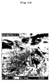
- Fig. 19 illustrates an atomic force microscopic image of an indentation acquired by the use of the diamond indenter; and
- Fig. 20 is an enlarged view of the atomic force microscopic image of the indentation acquired by the use of the diamond indenter. Also from Figs. 17 to 20, it is found that the resolution of the image acquired by the silicon probe is higher than that acquired by the diamond indenter, as described above.
- Figs. 16 to 18 reveals that a small quantity of carbide is present in a region 2 and no carbide is present at a pushed-in portion. Similarly, it is revealed that a largest quantity of carbide is present in a region 3 and the pushed-in portion is located just above carbide.
- the result of the indentation hardness measuring test illustrated in Fig. 21 shows that the hardness in the region 2 is lowest while the hardness in the region 3 is highest, and therefore, it is construed that the hardness depends upon the presence of carbide.
- the atomic force microscopic image of a high resolution is very useful in interpreting the curve expressing the relationship between the force and the penetration depth, and is very important for the research and development of the mechanical characteristics of the material in the minute region.
- the ultra micro indentation testing apparatus useful for the research and development of the functional material in the minute region.
- the mechanical properties of the fine structure of a semiconductor or an advanced functional material such as super steel will be elucidated to remarkably promote the development of such material.
- the indirect effect produced by the present invention is very profound in consideration of that only as small an installation space as that required by the conventional indentation hardness testing apparatus is required in spite of the testing apparatus having, in combination, all of the optical microscopic function, the atomic force microscopic function and the hardness measuring function, and that the testing apparatus having the functions in combination can be fabricated at a more reduced cost than that of independently fabricating apparatuses having respective functions.
Landscapes
- General Health & Medical Sciences (AREA)
- Health & Medical Sciences (AREA)
- Physics & Mathematics (AREA)
- Chemical & Material Sciences (AREA)
- General Physics & Mathematics (AREA)
- Immunology (AREA)
- Biochemistry (AREA)
- Analytical Chemistry (AREA)
- Life Sciences & Earth Sciences (AREA)
- Pathology (AREA)
- Nuclear Medicine, Radiotherapy & Molecular Imaging (AREA)
- Nanotechnology (AREA)
- Engineering & Computer Science (AREA)
- Radiology & Medical Imaging (AREA)
- Length Measuring Devices With Unspecified Measuring Means (AREA)
- Investigating Strength Of Materials By Application Of Mechanical Stress (AREA)
- Measurement Of Length, Angles, Or The Like Using Electric Or Magnetic Means (AREA)
- Instruments For Measurement Of Length By Optical Means (AREA)
- Length Measuring Devices By Optical Means (AREA)
Applications Claiming Priority (3)
| Application Number | Priority Date | Filing Date | Title |
|---|---|---|---|
| JP2000034225 | 2000-02-10 | ||
| JP2000034225A JP4008176B2 (ja) | 2000-02-10 | 2000-02-10 | 超微小押し込み試験装置 |
| PCT/JP2001/000927 WO2001059426A1 (en) | 2000-02-10 | 2001-02-09 | Superfine indentation tester |
Publications (2)
| Publication Number | Publication Date |
|---|---|
| EP1178299A1 true EP1178299A1 (de) | 2002-02-06 |
| EP1178299A4 EP1178299A4 (de) | 2005-02-23 |
Family
ID=18558598
Family Applications (1)
| Application Number | Title | Priority Date | Filing Date |
|---|---|---|---|
| EP01902821A Withdrawn EP1178299A4 (de) | 2000-02-10 | 2001-02-09 | Ultrafeine ritzprüfvorrichtung |
Country Status (6)
| Country | Link |
|---|---|
| US (1) | US6755075B2 (de) |
| EP (1) | EP1178299A4 (de) |
| JP (1) | JP4008176B2 (de) |
| KR (1) | KR100582015B1 (de) |
| CN (1) | CN1200261C (de) |
| WO (1) | WO2001059426A1 (de) |
Cited By (6)
| Publication number | Priority date | Publication date | Assignee | Title |
|---|---|---|---|---|
| WO2008042009A1 (en) | 2006-03-13 | 2008-04-10 | Asylum Research Corporation | Nanoindenter |
| EP1956607A1 (de) * | 2007-02-09 | 2008-08-13 | Korea Institute Of Machinery & Materials | AFM-Sonde von variabler Festigkeit |
| WO2011160863A1 (en) * | 2010-06-21 | 2011-12-29 | Closed Stock Company "Institute Of Applied Nanotechnology" | Scanning probe microscope with nanotome |
| CN102338714A (zh) * | 2011-03-07 | 2012-02-01 | 北京工业大学 | 生物软组织各向异性纳米压入测试台及利用该测试台进行纳米压入实验的方法 |
| US8857246B2 (en) | 2008-11-14 | 2014-10-14 | Atomic Energy Of Canada Limited | Portable polymer tester |
| EP3171153A1 (de) * | 2015-11-18 | 2017-05-24 | Anton Paar TriTec SA | Verfahren zur messung eines topografischen profils einer oberfläche einer probe und/oder eines topografischen bildes |
Families Citing this family (17)
| Publication number | Priority date | Publication date | Assignee | Title |
|---|---|---|---|---|
| US7121136B2 (en) * | 2002-12-25 | 2006-10-17 | Mitutoyo Corporation | Hardness testing apparatus |
| JP4229791B2 (ja) * | 2003-09-19 | 2009-02-25 | 真 金子 | 内視鏡装置 |
| EP1756835B1 (de) * | 2004-04-14 | 2012-08-29 | Veeco Instruments Inc. | Verfahren und vorrichtung zum erhalten von quantitativen messungen unter verwendung eines instruments auf sondenbasis |
| JP2005334985A (ja) * | 2004-05-24 | 2005-12-08 | Sii Nanotechnology Inc | 原子間力顕微鏡を用いた垂直断面加工方法 |
| DE602004016578D1 (de) * | 2004-07-02 | 2008-10-23 | Ernst Erik | Härteprüfgerät mit eindruck-prüfkörper aus hartmetall oder einer harten verbindung und schwingkronenstück zum testen bei hoher last sowie verfahren zur vergleichenden beurteilung des einhärtungsprofils |
| CN102288500B (zh) * | 2011-05-09 | 2013-04-10 | 中国人民解放军装甲兵工程学院 | 一种高精度仪器化压入仪及金刚石压头压入试样深度的计算方法 |
| JP5777957B2 (ja) * | 2011-07-05 | 2015-09-16 | 株式会社ミツトヨ | 硬さ試験機、及び硬さ試験方法 |
| JP5977556B2 (ja) * | 2012-03-27 | 2016-08-24 | 株式会社ミツトヨ | 硬さ試験機 |
| US20130319090A1 (en) * | 2012-05-30 | 2013-12-05 | Apple Inc. | Testing of surface crystalline content in bulk amorphous alloy |
| US9063048B2 (en) * | 2012-07-12 | 2015-06-23 | Mitutoyo Corporation | Hardness tester and program |
| EP2816342A1 (de) * | 2013-06-17 | 2014-12-24 | CSM Instruments SA | Messkopf für Nanoindentationsinstrument und Messverfahren |
| KR101558548B1 (ko) * | 2014-04-22 | 2015-10-13 | 한국지질자원연구원 | 자동 박편 연마 장치 |
| JP2017090071A (ja) * | 2015-11-04 | 2017-05-25 | 株式会社ミツトヨ | 硬さ試験機及び硬さ試験方法 |
| CH711792A2 (de) * | 2015-11-18 | 2017-05-31 | Anton Paar Tritec Sa | Verfahren zur Vermessung eines topographischen Profils und/oder eines topographischen Bildes einer Oberfläche einer Probe. |
| CN105547824B (zh) * | 2015-12-31 | 2018-07-06 | 爱德森(厦门)电子有限公司 | 一种在役设备原位材质检测装置及方法 |
| CN109238900B (zh) * | 2018-10-19 | 2024-02-27 | 四川大学 | 测头可贴附的金属微观表面磨蚀性检测设备以及测量方法 |
| JP7462181B2 (ja) * | 2019-11-29 | 2024-04-05 | 国立研究開発法人理化学研究所 | 三次元微小硬さ分布測定方法及び三次元微小硬さ分布測定システム |
Family Cites Families (7)
| Publication number | Priority date | Publication date | Assignee | Title |
|---|---|---|---|---|
| US4820051A (en) * | 1986-08-21 | 1989-04-11 | Nec Corporation | Apparatus for determining microhardness |
| US4852397A (en) * | 1988-01-15 | 1989-08-01 | Haggag Fahmy M | Field indentation microprobe for structural integrity evaluation |
| US5319960A (en) * | 1992-03-06 | 1994-06-14 | Topometrix | Scanning force microscope |
| US6026677A (en) * | 1993-10-01 | 2000-02-22 | Hysitron, Incorporated | Apparatus for microindentation hardness testing and surface imaging incorporating a multi-plate capacitor system |
| WO1996003641A1 (en) * | 1994-07-28 | 1996-02-08 | Kley Victor B | Scanning probe microscope assembly |
| JP2725741B2 (ja) | 1994-12-07 | 1998-03-11 | 科学技術庁金属材料技術研究所長 | 微小表面硬度測定装置 |
| JP2853687B2 (ja) | 1996-12-24 | 1999-02-03 | 日本電気株式会社 | 表面特性評価装置 |
-
2000
- 2000-02-10 JP JP2000034225A patent/JP4008176B2/ja not_active Expired - Lifetime
-
2001
- 2001-02-09 US US09/958,477 patent/US6755075B2/en not_active Expired - Fee Related
- 2001-02-09 EP EP01902821A patent/EP1178299A4/de not_active Withdrawn
- 2001-02-09 KR KR1020017012923A patent/KR100582015B1/ko not_active Expired - Fee Related
- 2001-02-09 WO PCT/JP2001/000927 patent/WO2001059426A1/ja not_active Application Discontinuation
- 2001-02-09 CN CNB018001998A patent/CN1200261C/zh not_active Expired - Fee Related
Cited By (9)
| Publication number | Priority date | Publication date | Assignee | Title |
|---|---|---|---|---|
| WO2008042009A1 (en) | 2006-03-13 | 2008-04-10 | Asylum Research Corporation | Nanoindenter |
| EP1994360A4 (de) * | 2006-03-13 | 2012-03-14 | Asylum Research Corp | Nanoindenter |
| EP1956607A1 (de) * | 2007-02-09 | 2008-08-13 | Korea Institute Of Machinery & Materials | AFM-Sonde von variabler Festigkeit |
| US7958566B2 (en) | 2007-02-09 | 2011-06-07 | Korea Institute Of Machinery & Materials | AFM probe with variable stiffness |
| US8857246B2 (en) | 2008-11-14 | 2014-10-14 | Atomic Energy Of Canada Limited | Portable polymer tester |
| US10107732B2 (en) | 2008-11-14 | 2018-10-23 | Atomic Energy Of Canada Limited | Portable polymer tester |
| WO2011160863A1 (en) * | 2010-06-21 | 2011-12-29 | Closed Stock Company "Institute Of Applied Nanotechnology" | Scanning probe microscope with nanotome |
| CN102338714A (zh) * | 2011-03-07 | 2012-02-01 | 北京工业大学 | 生物软组织各向异性纳米压入测试台及利用该测试台进行纳米压入实验的方法 |
| EP3171153A1 (de) * | 2015-11-18 | 2017-05-24 | Anton Paar TriTec SA | Verfahren zur messung eines topografischen profils einer oberfläche einer probe und/oder eines topografischen bildes |
Also Published As
| Publication number | Publication date |
|---|---|
| US20030070475A1 (en) | 2003-04-17 |
| KR100582015B1 (ko) | 2006-05-23 |
| CN1363036A (zh) | 2002-08-07 |
| CN1200261C (zh) | 2005-05-04 |
| JP2001221730A (ja) | 2001-08-17 |
| WO2001059426A1 (en) | 2001-08-16 |
| KR20020032420A (ko) | 2002-05-03 |
| JP4008176B2 (ja) | 2007-11-14 |
| US6755075B2 (en) | 2004-06-29 |
| EP1178299A4 (de) | 2005-02-23 |
Similar Documents
| Publication | Publication Date | Title |
|---|---|---|
| US6755075B2 (en) | Ultra micro indentation testing apparatus | |
| US8297130B2 (en) | Microtesting rig with variable compliance loading fibers for measuring mechanical properties of small specimens | |
| Chasiotis et al. | A new microtensile tester for the study of MEMS materials with the aid of atomic force microscopy | |
| Graham et al. | Topography and nanomechanical properties of tribochemical films derived from zinc dialkyl and diaryl dithiophosphates | |
| DE69817239T2 (de) | Optisches Nahfeld-Rastermikroskop | |
| Gao et al. | Construction and testing of a nanomachining instrument | |
| US20180024035A1 (en) | Apparatus for In-Line Testing and Surface Analysis on a Mechanical Property Tester | |
| Kiener et al. | Overview on established and novel FIB based miniaturized mechanical testing using in-situ SEM | |
| EP1985991B1 (de) | Messsonde, vorrichtung und verfahren zur oberflächenmessung einer probe | |
| Miyahara et al. | Evaluation of mechanical properties in nanometer scale using AFM-based nanoindentation tester | |
| EP2239556B1 (de) | Universaldurometer mit verbessertem Vertiefungslesegerät | |
| JP3675406B2 (ja) | マイクロ材料試験装置及びこれによる力学特性評価方法 | |
| JPS62245131A (ja) | ひつかき試験機 | |
| Tranchida et al. | Atomic force microscope nanoindentations to reliably measure the Young’s modulus of soft matter | |
| RU2510009C1 (ru) | Устройство для измерения параметров рельефа поверхности и механических свойств материалов | |
| JPH11230875A (ja) | 微小バネ定数測定装置およびバネ定数の測定方法 | |
| EP4273533A1 (de) | Dehnungsmessgerät und verfahren zur messung von mechanischen spannungen | |
| Randall et al. | Characterization of MEMS mechanical properties using nanoscale techniques | |
| JP2005201908A (ja) | マイクロ材料試験装置 | |
| Bergers | Anelasticity in Al-alloy thin films: an experimental analysis | |
| Li et al. | Towards Quantitative Characterisation of the Small Force Transducer Used in Nanoindentation Instruments | |
| Moharrami | Extracting reliable mechanical properties using the nanoindentation technique | |
| RU2653190C1 (ru) | Сканирующий зондовый микроскоп, совмещенный с устройством модификации поверхности образца | |
| Viswanathan | Evolution of friction coefficient during sliding of a single asperity on mineral/ceramic surfaces | |
| Rodolfo | COMPACT TEST PLATFORM FOR IN-SITU INDENTATION AND SCRATCHING INSIDE A SCANNING ELECTRON MICROSCOPE (SEM) |
Legal Events
| Date | Code | Title | Description |
|---|---|---|---|
| PUAI | Public reference made under article 153(3) epc to a published international application that has entered the european phase |
Free format text: ORIGINAL CODE: 0009012 |
|
| 17P | Request for examination filed |
Effective date: 20011109 |
|
| AK | Designated contracting states |
Kind code of ref document: A1 Designated state(s): AT BE CH CY DE DK ES FI FR GB GR IE IT LI LU MC NL PT SE TR |
|
| RBV | Designated contracting states (corrected) |
Designated state(s): DE FR GB |
|
| RAP1 | Party data changed (applicant data changed or rights of an application transferred) |
Owner name: JAPAN AS REPRESENTED BY DIRECTOR GENERAL OF NATION Owner name: JAPAN SCIENCE AND TECHNOLOGY AGENCY |
|
| A4 | Supplementary search report drawn up and despatched |
Effective date: 20050111 |
|
| STAA | Information on the status of an ep patent application or granted ep patent |
Free format text: STATUS: THE APPLICATION HAS BEEN WITHDRAWN |
|
| 18W | Application withdrawn |
Effective date: 20070806 |