EP1170869A2 - Method and arrangement for setting a frequency - Google Patents
Method and arrangement for setting a frequency Download PDFInfo
- Publication number
- EP1170869A2 EP1170869A2 EP01660120A EP01660120A EP1170869A2 EP 1170869 A2 EP1170869 A2 EP 1170869A2 EP 01660120 A EP01660120 A EP 01660120A EP 01660120 A EP01660120 A EP 01660120A EP 1170869 A2 EP1170869 A2 EP 1170869A2
- Authority
- EP
- European Patent Office
- Prior art keywords
- frequency
- divider
- vco
- voltage
- controlled oscillator
- Prior art date
- Legal status (The legal status is an assumption and is not a legal conclusion. Google has not performed a legal analysis and makes no representation as to the accuracy of the status listed.)
- Withdrawn
Links
- 238000000034 method Methods 0.000 title claims description 14
- 230000007423 decrease Effects 0.000 claims description 5
- 238000010586 diagram Methods 0.000 description 7
- 230000000694 effects Effects 0.000 description 3
- 238000013459 approach Methods 0.000 description 2
- 230000015572 biosynthetic process Effects 0.000 description 2
- 239000003990 capacitor Substances 0.000 description 2
- 230000003247 decreasing effect Effects 0.000 description 2
- 238000003786 synthesis reaction Methods 0.000 description 2
- 230000015556 catabolic process Effects 0.000 description 1
- 238000006731 degradation reaction Methods 0.000 description 1
- 238000004519 manufacturing process Methods 0.000 description 1
- 238000005259 measurement Methods 0.000 description 1
- 230000010355 oscillation Effects 0.000 description 1
- 230000035945 sensitivity Effects 0.000 description 1
- 230000001360 synchronised effect Effects 0.000 description 1
Images



Classifications
-
- H—ELECTRICITY
- H03—ELECTRONIC CIRCUITRY
- H03L—AUTOMATIC CONTROL, STARTING, SYNCHRONISATION OR STABILISATION OF GENERATORS OF ELECTRONIC OSCILLATIONS OR PULSES
- H03L7/00—Automatic control of frequency or phase; Synchronisation
- H03L7/06—Automatic control of frequency or phase; Synchronisation using a reference signal applied to a frequency- or phase-locked loop
- H03L7/16—Indirect frequency synthesis, i.e. generating a desired one of a number of predetermined frequencies using a frequency- or phase-locked loop
- H03L7/18—Indirect frequency synthesis, i.e. generating a desired one of a number of predetermined frequencies using a frequency- or phase-locked loop using a frequency divider or counter in the loop
- H03L7/197—Indirect frequency synthesis, i.e. generating a desired one of a number of predetermined frequencies using a frequency- or phase-locked loop using a frequency divider or counter in the loop a time difference being used for locking the loop, the counter counting between numbers which are variable in time or the frequency divider dividing by a factor variable in time, e.g. for obtaining fractional frequency division
- H03L7/199—Indirect frequency synthesis, i.e. generating a desired one of a number of predetermined frequencies using a frequency- or phase-locked loop using a frequency divider or counter in the loop a time difference being used for locking the loop, the counter counting between numbers which are variable in time or the frequency divider dividing by a factor variable in time, e.g. for obtaining fractional frequency division with reset of the frequency divider or the counter, e.g. for assuring initial synchronisation
-
- H—ELECTRICITY
- H03—ELECTRONIC CIRCUITRY
- H03L—AUTOMATIC CONTROL, STARTING, SYNCHRONISATION OR STABILISATION OF GENERATORS OF ELECTRONIC OSCILLATIONS OR PULSES
- H03L7/00—Automatic control of frequency or phase; Synchronisation
- H03L7/06—Automatic control of frequency or phase; Synchronisation using a reference signal applied to a frequency- or phase-locked loop
- H03L7/08—Details of the phase-locked loop
- H03L7/10—Details of the phase-locked loop for assuring initial synchronisation or for broadening the capture range
- H03L7/107—Details of the phase-locked loop for assuring initial synchronisation or for broadening the capture range using a variable transfer function for the loop, e.g. low pass filter having a variable bandwidth
- H03L7/1075—Details of the phase-locked loop for assuring initial synchronisation or for broadening the capture range using a variable transfer function for the loop, e.g. low pass filter having a variable bandwidth by changing characteristics of the loop filter, e.g. changing the gain, changing the bandwidth
-
- H—ELECTRICITY
- H03—ELECTRONIC CIRCUITRY
- H03L—AUTOMATIC CONTROL, STARTING, SYNCHRONISATION OR STABILISATION OF GENERATORS OF ELECTRONIC OSCILLATIONS OR PULSES
- H03L7/00—Automatic control of frequency or phase; Synchronisation
- H03L7/06—Automatic control of frequency or phase; Synchronisation using a reference signal applied to a frequency- or phase-locked loop
- H03L7/08—Details of the phase-locked loop
- H03L7/085—Details of the phase-locked loop concerning mainly the frequency- or phase-detection arrangement including the filtering or amplification of its output signal
- H03L7/089—Details of the phase-locked loop concerning mainly the frequency- or phase-detection arrangement including the filtering or amplification of its output signal the phase or frequency detector generating up-down pulses
- H03L7/0891—Details of the phase-locked loop concerning mainly the frequency- or phase-detection arrangement including the filtering or amplification of its output signal the phase or frequency detector generating up-down pulses the up-down pulses controlling source and sink current generators, e.g. a charge pump
-
- H—ELECTRICITY
- H03—ELECTRONIC CIRCUITRY
- H03L—AUTOMATIC CONTROL, STARTING, SYNCHRONISATION OR STABILISATION OF GENERATORS OF ELECTRONIC OSCILLATIONS OR PULSES
- H03L7/00—Automatic control of frequency or phase; Synchronisation
- H03L7/06—Automatic control of frequency or phase; Synchronisation using a reference signal applied to a frequency- or phase-locked loop
- H03L7/16—Indirect frequency synthesis, i.e. generating a desired one of a number of predetermined frequencies using a frequency- or phase-locked loop
- H03L7/18—Indirect frequency synthesis, i.e. generating a desired one of a number of predetermined frequencies using a frequency- or phase-locked loop using a frequency divider or counter in the loop
- H03L7/183—Indirect frequency synthesis, i.e. generating a desired one of a number of predetermined frequencies using a frequency- or phase-locked loop using a frequency divider or counter in the loop a time difference being used for locking the loop, the counter counting between fixed numbers or the frequency divider dividing by a fixed number
- H03L7/193—Indirect frequency synthesis, i.e. generating a desired one of a number of predetermined frequencies using a frequency- or phase-locked loop using a frequency divider or counter in the loop a time difference being used for locking the loop, the counter counting between fixed numbers or the frequency divider dividing by a fixed number the frequency divider/counter comprising a commutable pre-divider, e.g. a two modulus divider
Definitions
- the invention relates to a method for bringing a phase-locked loop into lock when the frequency setting of the loop changes.
- the invention further relates to an arrangement for bringing a phase-locked loop into lock.
- the phase-locked loop or PLL is a circuit in which feedback is used to, first, force the frequency of the oscillator in the circuit to follow the frequency of the input signal and, second, make the phase difference between the two waveforms in question constant. If the input signal is continuously varying, the PLL can be arranged to "seize" a certain frequency component. In telecommunications technology, the PLL is widely used for various synchronization purposes and frequency synthesis, for example. The latter is used in multichannel radio devices, such as mobile stations, to set the carrier frequency when selecting a channel.
- Fig. 1 shows an example of known circuit used for frequency synthesis. It includes the basic parts of the PLL, namely a phase difference detector 110, filter 120 and a voltage-controlled oscillator (VCO) 130. Connected to the first input R of the phase difference detector is a reference divider 141 to which a reference clock CK ref is brought from an external oscillator, the frequency f ref of the reference clock keeping constant with great accuracy.
- the reference divider will be called the r-divider for short.
- the division factor of the r-divider is m , which corresponds to an output frequency of f r .
- the loop is produced by the phase difference detector controlling the charge pump 150, the charge pump controlling the filter 120 and the filter controlling the VCO. Further, the output signal of the VCO is taken to a prescaler 142, the output signal of the prescaler is taken to a second divider 144, and the output signal of the latter is taken to the second input V of the phase difference detector.
- the said second divider will be called the v-divider for short.
- the frequency of the VCO is f vco
- the output frequency of the prescaler is f'
- the output frequency of the v-divider is f v .
- the division ratio of the v-divider is n
- the division ratio of the auxiliary divider is a .
- These three counters are interconnected in a known manner such that during the v-divider cycle the prescaler divides its input frequency by a number p for a clock cycle amount n-a of the auxiliary divider.
- the prescaler divides the frequency by a number p +1.
- the number of VCO cycles during the v-divider cycle is p(n-a) + (p+1)a.
- f 0 pnf r .
- the phase difference detector 110 has got two outputs U and D.
- the phase of the first input R leads the second input V, there appear “0" pulses at the frequency of f r at the output U, the length of the said pulses being proportional to the phase difference between the input signals.
- Output D remains in state "0".
- the phase of the first input R lags behind the second input V, there appear “1” pulses at the frequency of f r at the output D, the length of the said pulses being proportional to the phase difference between the input signals.
- Output U remains in state "1".
- Output U controls the upper switch component Q1 in the charge pump 150 in such a manner that the Q1 passes during a U pulse the current of the current source J1, connected in series with the switch Q1, from the positive terminal of the operating voltage supply to the filter 120.
- Output D controls the lower switch component Q2 in the charge pump 150 in such a manner that the Q2 passes during a D pulse the current of the current source J2, connected in series with the switch Q2, from the filter 120 to ground.
- the filter 120 includes a series connection of a capacitor C1 and resistor R1 as well as a capacitor C2 in parallel with the said series connection. Filter component values are chosen such that the filter impedance at frequency f r is determined only by resistance R1.
- capacitance C1 raises the magnitude of the filter impedance
- capacitance C2 lowers the magnitude of the filter impedance.
- the effect of the capacitances may also be expressed by saying that they smooth out the shape of the voltage coming from the charge pump.
- the filter voltage v c has a certain positive level.
- the said U pulses raise this voltage level and the said D pulses lower it.
- the oscillator 130 is controlled by the voltage v c .
- the increase in the control voltage results in an increase in the frequency f vco and vice versa.
- a disadvantage of circuits like those described above is that the locking of the loop may take too long a time when the frequency is changed.
- a high locking speed is required e.g. when transmitting data in several time slots belonging to different frequency division channels, whereby changes between channels are sometimes relatively rapid.
- An insufficient speed in the loop may be caused by the slowness of the filter in the circuit. However, making the filter faster would degrade the noise characteristics of the loop.
- the insufficient speed of the loop may be caused by too low input frequency in the phase difference detector.
- frequency correction advances in steps: Each individual subcorrection is based on a comparison carried out during one cycle of the input frequency f r .
- the settling speed of the VCO frequency can in a known manner be increased using a so-called fractional-N structure.
- the output frequency of the VCO can be changed in steps that are only a certain fraction of the reference input frequency of the phase difference detector.
- the reference input frequency may then be greater compared to a corresponding structure according to Fig. 1, which means a higher settling speed.
- a disadvantage of the fractional-N circuit is its complicity, resulting in a relatively large size and high manufacturing cost.
- Fig. 2 shows the block diagram of the structure. It is based on a structure like the one shown in Fig. 1, comprising an r-divider 241, phase difference detector 210, charge pump 250, low-pass filter 220, voltage-controlled oscillator 230 and a divider unit 240. The latter corresponds to the dividers 142, 143 and 144 in Fig. 1.
- the circuit further includes a block called 'frequency detector method speedup circuit', FDMSC for short, and a switch SWI for the low-pass filter.
- the input signals of the FDMSC are the same output signals R and V of the r-divider and divider unit 240 that are also taken to the phase difference detector, and the output signals U and D of the phase difference detector.
- the output signals of the FDMSC are the control signals U' and D' of the charge pump 250, the reset signal of the r-divider and divider unit 240, and the control signal for the switch SWI.
- the FDMSC When the frequency setting changes in the divider unit 240, the FDMSC observes a difference between the frequencies f r and f v of signals R and V and connects to the charge pump a constant control signal U' or D', depending on the direction in which the VCO frequency has to be changed. So at this stage the output signals U and D of the phase difference detector 210 have no effect on the operation of the loop. In addition, the FDMSC closes the switch SWI. This switching substantially decreases the time constant of the low-pass filter 220, increasing the speed of change of the filter output voltage.
- the FDMSC opens the switch SWI, returns the charge pump control to the normal state, and resets the r-divider 241 and divider unit 240. After that, the phase difference detector again indicates a phase difference between the signals R and V, and the loop locks.
- the reduction of the duration of the frequency change phase in the circuit of Fig. 2 is based on using continuous control for the charge pump in the change phase instead of pulse control and, on the other hand, speeding up the loop filter.
- a disadvantage of the circuit is that the FDMSC means a relatively large addition in the loop logic.
- An object of the invention is to reduce the said disadvantages associated with the prior art.
- the method according to the invention is characterized by that which is specified in the independent claim 1.
- the structure according to the invention is characterized by that which is specified in the independent claim 6.
- the basic idea of the invention is that the locking speed of the loop is improved at the expense of noise characteristics.
- the degradation of noise characteristics is momentary only, so it is of no importance when using the frequency produced by the structure.
- the counters dividing the reference frequency and VCO frequency are made to count simultaneously from zero.
- the length of the first output pulse of the phase difference detector corresponds to the difference between the new frequency and the old frequency.
- the loop filter is switched so as to become a purely capacitive circuit the output voltage of which changes in proportion to the length of the pulse from the phase difference detector.
- the loop parameters are selected such that the voltage difference produced during the said pulse produces directly in the VCO frequency a change of the correct magnitude.
- the frequency correction cycle described above may be repeated a couple of times, just to be on the safe side.
- An advantage of the invention is that the loop locks onto the new frequency more quickly than in the prior art.
- Another advantage of the invention is that its implementation is relatively simple, i.e. it requires relatively few additional circuits.
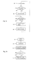
- Fig. 3a shows a flow diagram on the control of divider counter according to the invention.
- the method can be applied e.g. to the r-divider 141 and prescaler 142, v-divider 144 and auxiliary divider 143 shown in Fig. 1. Let the divider formed by the latter three together be called the vco-divider.
- the dividers are counting their clock pulses. During the counting it is monitored in accordance with step 301 whether the r-divider or vco-divider cycle is completed. When either of these two cycles is completed, the reset of the divider in question is set in accordance with step 302. In step 303 the cycle of the other of the said dividers is awaited to be completed.
- step 304 the reset of that other divider is also set in accordance with step 304.
- step 305 both resets are removed, synchronized with the reference clock CK ref , for example.
- both the r-divider and vco-divider start counting simultaneously from zero up.
- the phase difference detector outputs a pulse which starts upon the completion of the cycle of the first divider and lasts up to the completion of the cycle of the second divider.
- the output pulse of the phase difference detector produces separately at every cycle the information on the frequency difference between the input frequencies. This information can be used for speeding up the settling of the VCO frequency.
- the phase difference detector produces the phase difference information but it does not reveal the frequency difference.
- the VCO frequency settles at a certain relatively low speed.
- Fig. 3b shows an example of the second part of the method according to the invention.
- the operation starts from a situation 310 in which the PLL is given a new frequency setting.
- the r-divider and vco-divider are reset, step 311.
- step 312 a change is made in the loop filter, which change is essential as regards the invention:
- the resistive part of the filter is bypassed so that only the capacitive part remains. Thereby the voltage of the circuit changes almost linearly when a constant current is fed into it or sunk from it.
- the speed of change of the voltage of the filter circuit is increased in order to speed up VCO control.
- step 313 time is counted. When a certain time ⁇ t has elapsed, the filter circuit is restored into its normal mode and its speed of change of voltage is returned to the lower value.
- the time ⁇ t corresponds to the VCO frequency settling time; it is e.g. two or three cycle times of the input signals of the phase difference detector.
- Fig. 4 shows an example of the implementation of the PLL according to the invention.
- the circuit is otherwise like the one in Fig. 1 except that it further comprises a divider reset unit 445 and filter switch SW with a control unit SWC.
- the reset unit 445 has got three D flip-flops and an AND gate.
- the clock input of the first flip-flop ff1 is connected to the output R of the r-divider 441, the D input is fixed to "1", and the output Q is connected to the reset input of the r-divider and to the first input of the AND gate.
- the clock input of the second flip-flop ff2 is connected to the output V of the v-divider 444, the D input is fixed to "1", and the output Q is connected to the reset inputs of the v-divider and prescaler 442 and to the second input of the AND gate.
- the output of the AND gate is connected to the D input of the third flip-flop ff3.
- the clock input of the flip-flop ff3 is connected to the output CK ref of the reference oscillator, and the output Q is connected to the reset input of the first and second flip-flop. Then, when the r-divider cycle is completed and the output R changes into "1", the first flip-flop sets the r-divider reset.
- the second flip-flop sets the v-divider and prescaler resets.
- the output of the third flip-flop is set to "1", resulting in the removal of the divider resets. So, the operation is in accordance with Fig. 3a.
- the logic of the reset unit 445 is naturally presented by way of example only.
- the filter 420 has a switch component SW.
- the state of the switch component is determined by the output signal S of the switch control unit SWC.
- the signal S is at the same time set to "0", whereby the switch SW starts to conduct and the filter 420 becomes almost purely capacitive.
- signal S is further used to control the current sources J1, J2 in the charge pump 450.
- S is "1"
- the source current I has a value I 1
- S is "0"
- the source current I has a value I 2 .
- Value I 2 is greater than value I 1 whereby the frequency of the VCO changes during the frequency correction more quickly than in the circuit according to Fig. 1.
- the change in the source current is brought about by changing, by means of switches, the structure of an individual current source J1, J2 or by connecting another current source in parallel with them.
- a count is started in the switch control unit SWC, and after a certain amount of cycles of the input signal V of the phase difference detector the control unit SWC returns to the normal state, making the switch SW non-conductive and setting the source current I to its lower value.
- the operation is thus in accordance with Fig. 3b.
- the generation of the control signal S as described above, is naturally presented by way of example only. Signal S could be provided direct from an external processor, in which case the control unit SWC would not be required at all.
- Fig. 5 shows a pulse diagram example of the operation of the circuit according to the invention. It shows from top down the variations in the following signals: r-divider output R, r-divider reset reset-r , v-divider output V, v-divider reset reset-v, and the second output U of the phase difference detector.
- the diagram starts at moment t 0 when an external processor issues a new frequency setting for the PLL. This results also in the resetting of the dividers so that the dividers simultaneously begin to count from zero. Before setting the frequency the loop was in lock and the cycle lengths T r and T v of the r-divider and v-divider were equal. In the example depicted, the VCO frequency is to be increased, whereby the division ratio pn+a becomes greater.
- a pulse is generated at the phase difference detector's output U. It starts from the leading edge of signal R and ends at the leading edge of signal V.
- the length ⁇ 1 of the first U pulse is thus the difference T v1 -T r .
- the length ⁇ 1 of the pulse is proportional to the frequency change desired. Additionally, it depends on the VCO frequency prior to the frequency change. Therefore, the analog parts of the loop are chosen such that the control is at its most accurate at the center of the range of variation of the VCO frequency.
- the v-divider cycle will be completed before the r-divider cycle. In that case the phase difference detector will issue a D pulse proportional to the frequency difference, causing the VCO control voltage and frequency f vco to drop.
- Fig. 6 illustrates the settling of the VCO frequency in the PLL according to the invention and in a PLL according to the prior art.
- Time reference designators t 0 to t 4 correspond to the reference designators of Fig. 5.
- Plot 61 corresponds to the pulse diagram of Fig. 5.
- the VCO frequency at moment t 0 and from that moment on up till moment t 1 is f i .
- From t 1 to t 2 the frequency f vco increases near to its newly set value f j .
- From t 2 to t 3 the frequency f vco remains constant as the frequency error is being measured by means of the r-divider and vco-divider and phase difference detector.
- Plot 62 depicts the typical VCO frequency change in a prior-art PLL.
- the frequency approaches its set value relatively slowly, due to the loop characteristics chosen according to the noise and stability requirements.
- the frequency change continues after the set value has been reached, and then approaches it again, this time from above. Final settling takes place only after several oscillations.
- Plot 61 illustrates the advantage of the invention, when applied to an ordinary frequency synthesizer implemented using a PLL.
- a prior-art circuit according to Fig. 2 may achieve similar results as the present invention.
- the implementation of the circuit shown in Fig. 2 differs from the present invention:
- the cut-off frequency of the loop filter is increased by means of a switch in order to speed up the filter.
- the filter is turned into a capacitive circuit so that the VCO control voltage changes linearly and in direct proportion to the frequency difference during a control pulse.
- FDMSC additional logic
- the filter control is set.
- the frequency difference is measured immediately after the new frequency setting by means of logic that is already included in the structure for the most part, and a control pulse corresponding to the measurement result is then issued to the VCO.
Landscapes
- Stabilization Of Oscillater, Synchronisation, Frequency Synthesizers (AREA)
Abstract
Description
- Fig. 1
- shows an example of the frequency synthesizer according to the prior art,
- Fig. 2
- shows another example of the frequency synthesizer according to the prior art,
- Figs. 3a,b
- illustrate in the form of flow diagram the method according to the invention,
- Fig. 4
- shows an example of the circuit according to the invention,
- Fig. 5
- illustrates in the form of pulse diagram an example of the operation of the circuit according to the invention, and
- Fig. 6
- shows a comparison between the locking of a loop according to the prior art and the locking of the loop according to the invention.
- I2 =
- current of charge pump current sources during frequency correction,
- C =
- filter circuit capacitance,
- Δf =
- difference between the new and old frequency,
- kv =
- VCO sensitivity (Hz/V), and
- τ =
- length of the first pulse coming from phase difference detector after the frequency setting.
Claims (13)
- A method for setting a frequency in a phase locked loop having, in that order, a reference divider to decrease a reference frequency, phase difference detector, a charge pump, a filter, a voltage-controlled oscillator, and a programmable vco-divider to decrease the frequency produced by the voltage-controlled oscillator, which method comprises the steps ofcomparing the phases of the signals output by the reference divider and vco-divider,processing the signal produced by the said comparison andcontrolling said oscillator with the signal produced by the processing mentioned above, andresetting the reference divider and vco-divider after the new frequency setting has been made in the programmable vco-divider, characterized in that after the new frequency setting has been made, the following actions are taken at least during the first cycle of the reference divider:the difference between the frequency set for the voltage-controlled oscillator and the actual frequency thereof is measured, andthe control voltage of the voltage-controlled oscillator is changed proportionally to the frequency difference measured substantially by an amount corresponding thereto.
- A method according to claim 1, characterized in that in order to measure the said frequency difference,the reference divider reset is set (302; 304) when the state of its output signal has changed as the cycle of the divider counter in question is completed,the vco-divider reset is set (302; 304) when the state of its output signal has changed as the cycle of the divider counter in question is completed, andthe said resets are removed (305) when both the reference divider and the vco-divider are in the reset state.
- A method according to claim 1, characterized in that in order to change the control voltage of the voltage-controlled oscillator proportionally to the said frequency difference the said filter is turned (312) into a circuit the voltage of which changes substantially linearly when a direct current flows into or out of the circuit.
- A method according to claims 1 and 3, characterized in that in order to change the control voltage of the voltage-controlled oscillator by an amount corresponding substantially to the said frequency difference, the speed of change of the voltage of the said filter circuit turned linear is increased (312).
- A method according to claim 4, characterized in that in order to increase the speed of change of the voltage of the filter circuit the current of the current sources in the said charge pump is increased.
- An arrangement for setting a frequency in a phase locked loop having, in that order, a reference divider (441) to decrease a reference frequency, phase difference detector (410), charge pump (450), filter (420), voltage-controlled oscillator (430), and a programmable vco-divider (442, 443, 444) to decrease the frequency produced by the voltage-controlled oscillator, and a means for resetting the reference divider and vco-divider after the new frequency setting has been made in the programmable vco-divider, characterized in that it comprises means for measuring the difference between the frequency set for the voltage-controlled oscillator and the actual frequency thereof during a single cycle of the reference divider, and means for changing the control voltage of the voltage-controlled oscillator proportionally to the frequency difference measured by an amount substantially corresponding thereto.
- An arrangement according to claim 6, characterized in that the said means for measuring the frequency difference comprises the said reference divider, programmable vco-divider and phase difference detector, and additionally a reset unit (445) for the reference divider and vco-divider.
- An arrangement according to claim 7, characterized in that the said reset unit for the reference divider and vco-divider comprises a first memory element (ff1) for setting a reset for the reference divider when the state of the output signal (R) of the reference divider has changed as its cycle is completed, a second memory element (ff2) for setting a reset for the vco-divider when the state of the output signal (V) of the vco-divider has changed as its cycle is completed, and a circuit (&, ff3) for removing the said settings of the first and second memory elements when both the reference divider and the vco-divider are in the reset state.
- An arrangement according to claim 6, characterized in that the said means for changing the control voltage of the voltage-controlled oscillator proportionally to the said frequency difference comprises in parallel with the resistive part (R1) of the filter a first switch (SW) that turns the said filter into a substantially capacitive circuit (C1, C2).
- An arrangement according to claim 6, characterized in that the said means for changing the control voltage of the voltage-controlled oscillator by an amount substantially corresponding to the said frequency difference comprises a switch circuit for changing the source currents in the said charge pump.
- An arrangement according to claims 6, 9 and 10, characterized in that the said means for changing the control voltage of the voltage-controlled oscillator proportionally to the measured frequency difference by an amount substantially corresponding thereto further comprises control means for the said first switch and the said switch circuit, said control means being arranged so as to close the first switch and to make the said source currents larger after the new frequency setting has been made, and to open the first switch and make the said source currents smaller again after a certain period of time from the new frequency setting.
- An arrangement according to claim 11, characterized in that the said control means for the first switch and switch circuit comprises a logic unit (425).
- An arrangement according to claim 11, characterized in that the said control means for the first switch and switch circuit comprises a program in a processor outside the phase-locked loop.
Applications Claiming Priority (2)
| Application Number | Priority Date | Filing Date | Title |
|---|---|---|---|
| FI20001557A FI108688B (en) | 2000-06-30 | 2000-06-30 | Method and arrangement for setting the frequency |
| FI20001557 | 2000-06-30 |
Publications (2)
| Publication Number | Publication Date |
|---|---|
| EP1170869A2 true EP1170869A2 (en) | 2002-01-09 |
| EP1170869A3 EP1170869A3 (en) | 2003-08-13 |
Family
ID=8558683
Family Applications (1)
| Application Number | Title | Priority Date | Filing Date |
|---|---|---|---|
| EP01660120A Withdrawn EP1170869A3 (en) | 2000-06-30 | 2001-06-25 | Method and arrangement for setting a frequency |
Country Status (3)
| Country | Link |
|---|---|
| US (1) | US6661293B2 (en) |
| EP (1) | EP1170869A3 (en) |
| FI (1) | FI108688B (en) |
Cited By (2)
| Publication number | Priority date | Publication date | Assignee | Title |
|---|---|---|---|---|
| US7023285B2 (en) | 2003-07-15 | 2006-04-04 | Telefonaktiebolaget Lm Ericsson (Publ) | Self-calibrating controllable oscillator |
| EP3764547A1 (en) * | 2019-07-09 | 2021-01-13 | STMicroelectronics (Rousset) SAS | Method for managing the starting of a phase locking loop, and corresponding integrated circuit |
Families Citing this family (6)
| Publication number | Priority date | Publication date | Assignee | Title |
|---|---|---|---|---|
| US7242229B1 (en) | 2001-05-06 | 2007-07-10 | Altera Corporation | Phase locked loop (PLL) and delay locked loop (DLL) counter and delay element programming in user mode |
| GB0202884D0 (en) * | 2002-02-07 | 2002-03-27 | Nokia Corp | Synthesiser |
| ITMI20050138A1 (en) * | 2005-01-31 | 2006-08-01 | St Microelectronics Srl | METHOD AND FLL-PLL SYSTEM FREQUENCY LOCK LOOP-PHASE LOCK LOOP COMPLETELY DIGITAL WITH A BRIEF LOCKING TIME |
| US7902886B2 (en) * | 2007-10-30 | 2011-03-08 | Diablo Technologies Inc. | Multiple reference phase locked loop |
| CN103259536B (en) * | 2012-02-20 | 2018-12-18 | 德克萨斯仪器股份有限公司 | Eliminate the device of charge pump phase lock loop road loop filter resistor noise |
| US8593188B2 (en) * | 2012-02-20 | 2013-11-26 | Texas Instruments Incorporated | Apparatus to remove the loop filter resistor noise in charge-pump PLL |
Family Cites Families (13)
| Publication number | Priority date | Publication date | Assignee | Title |
|---|---|---|---|---|
| JP3077151B2 (en) * | 1990-02-13 | 2000-08-14 | 日本電気株式会社 | Frequency synthesis method and frequency synthesizer |
| JPH04297128A (en) * | 1991-03-26 | 1992-10-21 | Hitachi Denshi Ltd | PLL circuit |
| BR9406065A (en) | 1993-11-09 | 1996-02-06 | Motorola Inc | Process and apparatus for suppression of phase or frequency error. |
| EP0755120A1 (en) | 1995-07-18 | 1997-01-22 | Nec Corporation | Phase-locked loop circuit |
| US5933058A (en) * | 1996-11-22 | 1999-08-03 | Zoran Corporation | Self-tuning clock recovery phase-locked loop circuit |
| JPH1168559A (en) | 1997-08-20 | 1999-03-09 | Nec Corp | Phase-locked loop circuit |
| US6236275B1 (en) * | 1997-10-24 | 2001-05-22 | Ericsson Inc. | Digital frequency synthesis by sequential fraction approximations |
| GB2341285B (en) * | 1998-09-02 | 2001-12-19 | Nec Technologies | Frequency synthesisers |
| JP3384755B2 (en) * | 1998-11-26 | 2003-03-10 | 三洋電機株式会社 | PLL synthesizer circuit |
| EP1030453A1 (en) | 1999-01-20 | 2000-08-23 | Sony International (Europe) GmbH | A method for reducing transition time in a PLL frequency synthesizer having a programmable frequency divider |
| JP2000278124A (en) | 1999-03-26 | 2000-10-06 | Sanyo Electric Co Ltd | Pll circuit |
| US6420917B1 (en) * | 1999-10-01 | 2002-07-16 | Ericsson Inc. | PLL loop filter with switched-capacitor resistor |
| US6466069B1 (en) * | 2000-11-21 | 2002-10-15 | Conexant Systems, Inc. | Fast settling charge pump |
-
2000
- 2000-06-30 FI FI20001557A patent/FI108688B/en active
-
2001
- 2001-06-25 EP EP01660120A patent/EP1170869A3/en not_active Withdrawn
- 2001-06-28 US US09/894,185 patent/US6661293B2/en not_active Expired - Lifetime
Cited By (4)
| Publication number | Priority date | Publication date | Assignee | Title |
|---|---|---|---|---|
| US7023285B2 (en) | 2003-07-15 | 2006-04-04 | Telefonaktiebolaget Lm Ericsson (Publ) | Self-calibrating controllable oscillator |
| EP3764547A1 (en) * | 2019-07-09 | 2021-01-13 | STMicroelectronics (Rousset) SAS | Method for managing the starting of a phase locking loop, and corresponding integrated circuit |
| FR3098665A1 (en) * | 2019-07-09 | 2021-01-15 | Stmicroelectronics (Rousset) Sas | Method for managing the start of a phase-locked loop, and corresponding integrated circuit |
| US11115038B2 (en) | 2019-07-09 | 2021-09-07 | Stmicroelectronics (Rousset) Sas | Method for managing the startup of a phase-locked loop and corresponding integrated circuit |
Also Published As
| Publication number | Publication date |
|---|---|
| EP1170869A3 (en) | 2003-08-13 |
| FI20001557A0 (en) | 2000-06-30 |
| US6661293B2 (en) | 2003-12-09 |
| FI108688B (en) | 2002-02-28 |
| US20020000884A1 (en) | 2002-01-03 |
Similar Documents
| Publication | Publication Date | Title |
|---|---|---|
| US9042854B2 (en) | Apparatus and methods for tuning a voltage controlled oscillator | |
| US7982552B2 (en) | Automatic frequency calibration apparatus and method for a phase-locked loop based frequency synthesizer | |
| JP3587818B2 (en) | Phase control circuit | |
| US7295078B2 (en) | High-speed, accurate trimming for electronically trimmed VCO | |
| KR100847687B1 (en) | Frequency Synthesizer and Frequency Control Method | |
| KR100361855B1 (en) | Frequency synthesizer | |
| US7372339B2 (en) | Phase lock loop indicator | |
| JPH11195983A (en) | Integrated circuit having phase locked loop | |
| US8125253B2 (en) | System and method for dynamically switching between low and high frequency reference clock to PLL and minimizing PLL output frequency changes | |
| EP1583241B1 (en) | Phase locked loop frequency synthesizer | |
| CN110999087B (en) | Phase-locked loop circuit | |
| KR100831651B1 (en) | Calibrating a loop-filter of a phase locked loop | |
| US6661293B2 (en) | Method and arrangement for setting a frequency | |
| CN107820681A (en) | Fast coarse and fine tuning calibration of multi-curve calibrated synthesizer within target window | |
| US5821789A (en) | Fast switching phase-locked loop | |
| CN117691993A (en) | A voltage-controlled oscillator circuit and adjustment method with synchronous and adaptive frequency and amplitude | |
| US20260081614A1 (en) | Interpolative divider | |
| EP1897221B1 (en) | Phase-locked loop systems using adaptive low-pass filters in switched bandwidth feedback loops | |
| US7023285B2 (en) | Self-calibrating controllable oscillator | |
| EP1538451B1 (en) | Phase -locked loop with a programmable frequency detector | |
| US7439812B1 (en) | Auto-ranging phase-locked loop | |
| JP2004080624A (en) | Frequency synthesizer | |
| JPH07221641A (en) | Frequency synthesizer | |
| KR20000061182A (en) | Phase locked loop having a performance of high speed responce | |
| JP2003152531A (en) | Pll circuit |
Legal Events
| Date | Code | Title | Description |
|---|---|---|---|
| PUAI | Public reference made under article 153(3) epc to a published international application that has entered the european phase |
Free format text: ORIGINAL CODE: 0009012 |
|
| AK | Designated contracting states |
Kind code of ref document: A2 Designated state(s): AT BE CH CY DE DK ES FI FR GB GR IE IT LI LU MC NL PT SE TR |
|
| AX | Request for extension of the european patent |
Free format text: AL;LT;LV;MK;RO;SI |
|
| RAP1 | Party data changed (applicant data changed or rights of an application transferred) |
Owner name: NOKIA CORPORATION |
|
| PUAL | Search report despatched |
Free format text: ORIGINAL CODE: 0009013 |
|
| AK | Designated contracting states |
Designated state(s): AT BE CH CY DE DK ES FI FR GB GR IE IT LI LU MC NL PT SE TR |
|
| AX | Request for extension of the european patent |
Extension state: AL LT LV MK RO SI |
|
| AKX | Designation fees paid | ||
| REG | Reference to a national code |
Ref country code: DE Ref legal event code: 8566 |
|
| STAA | Information on the status of an ep patent application or granted ep patent |
Free format text: STATUS: THE APPLICATION IS DEEMED TO BE WITHDRAWN |
|
| 18D | Application deemed to be withdrawn |
Effective date: 20040214 |