EP1170853A2 - Einphasengleichstromrichter mit Leistungsfaktorregelungsfunktion - Google Patents
Einphasengleichstromrichter mit Leistungsfaktorregelungsfunktion Download PDFInfo
- Publication number
- EP1170853A2 EP1170853A2 EP01115650A EP01115650A EP1170853A2 EP 1170853 A2 EP1170853 A2 EP 1170853A2 EP 01115650 A EP01115650 A EP 01115650A EP 01115650 A EP01115650 A EP 01115650A EP 1170853 A2 EP1170853 A2 EP 1170853A2
- Authority
- EP
- European Patent Office
- Prior art keywords
- output
- circuit
- rectifying
- power supply
- smoothing
- Prior art date
- Legal status (The legal status is an assumption and is not a legal conclusion. Google has not performed a legal analysis and makes no representation as to the accuracy of the status listed.)
- Withdrawn
Links
Images


Classifications
-
- H—ELECTRICITY
- H02—GENERATION; CONVERSION OR DISTRIBUTION OF ELECTRIC POWER
- H02M—APPARATUS FOR CONVERSION BETWEEN AC AND AC, BETWEEN AC AND DC, OR BETWEEN DC AND DC, AND FOR USE WITH MAINS OR SIMILAR POWER SUPPLY SYSTEMS; CONVERSION OF DC OR AC INPUT POWER INTO SURGE OUTPUT POWER; CONTROL OR REGULATION THEREOF
- H02M1/00—Details of apparatus for conversion
- H02M1/42—Circuits or arrangements for compensating for or adjusting power factor in converters or inverters
- H02M1/4208—Arrangements for improving power factor of AC input
- H02M1/4225—Arrangements for improving power factor of AC input using a non-isolated boost converter
-
- H—ELECTRICITY
- H02—GENERATION; CONVERSION OR DISTRIBUTION OF ELECTRIC POWER
- H02M—APPARATUS FOR CONVERSION BETWEEN AC AND AC, BETWEEN AC AND DC, OR BETWEEN DC AND DC, AND FOR USE WITH MAINS OR SIMILAR POWER SUPPLY SYSTEMS; CONVERSION OF DC OR AC INPUT POWER INTO SURGE OUTPUT POWER; CONTROL OR REGULATION THEREOF
- H02M7/00—Conversion of ac power input into dc power output; Conversion of dc power input into ac power output
- H02M7/02—Conversion of ac power input into dc power output without possibility of reversal
- H02M7/04—Conversion of ac power input into dc power output without possibility of reversal by static converters
- H02M7/05—Capacitor coupled rectifiers
-
- Y—GENERAL TAGGING OF NEW TECHNOLOGICAL DEVELOPMENTS; GENERAL TAGGING OF CROSS-SECTIONAL TECHNOLOGIES SPANNING OVER SEVERAL SECTIONS OF THE IPC; TECHNICAL SUBJECTS COVERED BY FORMER USPC CROSS-REFERENCE ART COLLECTIONS [XRACs] AND DIGESTS
- Y02—TECHNOLOGIES OR APPLICATIONS FOR MITIGATION OR ADAPTATION AGAINST CLIMATE CHANGE
- Y02B—CLIMATE CHANGE MITIGATION TECHNOLOGIES RELATED TO BUILDINGS, e.g. HOUSING, HOUSE APPLIANCES OR RELATED END-USER APPLICATIONS
- Y02B70/00—Technologies for an efficient end-user side electric power management and consumption
- Y02B70/10—Technologies improving the efficiency by using switched-mode power supplies [SMPS], i.e. efficient power electronics conversion e.g. power factor correction or reduction of losses in power supplies or efficient standby modes
Definitions
- the present invention relates to a single phase AC-DC converter, and particularly, relates to a single phase AC-DC converter having a construction that a PFC (Power Factor Control) power supply section, where a rectified current obtained by rectifying an electric current from an AC supply is switched, and a DC-DC power supply section, where a direct current obtained by rectifying and smoothing an electric current from an AC supply is switched, are combined together; the switching elements for switching both the sections are driven and controlled with only one servo loop.
- PFC Power Factor Control
- the present inventor discloses a single phase AC-DC converter where a PFC power supply section and a DC-DC power supply section are combined together in Japanese Patent Preliminarily Publication No. 11-356046.
- a PFC switching power supply section (rectified current side) having a smaller current smoothing function and a DC-DC switching power supply section (direct current side) having a greater current smoothing function are combined in a parallel manner; the rectified outputs of these sections are added together; thereby a harmonics current can be restricted ,the size of the converter becomes compact, and a high efficiency can be obtained.
- the rectified current side contributes to restrict a harmonics current, while the direct current side keeps a holding time sufficiently and reduces a ripple voltage.
- so-called two-stage type AC-DC converters which also have a PFC power supply section and a DC-DC power supply section being connected together in a cascade manner in order to restrict a harmonics current.
- the current International Standard for harmonics current is IEC61000-3-2.
- the current waveform belongs to the Class A of the IEC62000-3-2, so that the converter satisfies the harmonics spectrum standard defined by the Class A without problem.
- an AC-DC converter comprises a PFC power supply section where a rectified current obtained by rectifying an electric current from an AC supply is switched, a DC-DC power supply section where a direct current obtained by rectifying and smoothing an electric current from an AC supply is switched, a first switching means for conducting a switching operation in said PFC power supply section, a second switching means for conducting a switching operation in said DC-DC power supply section, a drive pulse generating circuit for generating first drive pulses for driving said first switching means and second drive pulses for driving said second switching means, and a servo loop for controlling said drive pulse generating circuit; wherein said servo loop is constituted of only one serve loop; and wherein said converter comprises a duty ratio controlling means for making a duty ratio (ON time) of said drive pulses for driving said first switching means and a duty ratio (ON time) of said drive pulses for driving said second switching means different from each other in a linked manner.
- a duty ratio controlling means is provided, by which the duty ratio (ON time) of the drive pulses for driving the first switching means and the duty ratio (ON time) of the drive pulses for driving the second switching means become different from each other in a linked manner, so that efficiency is improved and the size of the converter can be made compact.
- the AC-DC converter according to the present invention has a characteristic in that said PFC power supply section comprises an input for connection to a source of a single phase AC supply, a first rectifying circuit for rectifying an electric current supplied from said inputs, a first transformer where one end of the primary coil thereof is connected to an output of said rectifying circuit and the other end of said primary coil is connected to said first switching means, and a first secondary side rectifying circuit for rectifying an output of the secondary side of said first transformer; said DC-DC power supply section comprises an input for connection to a source of a single phase AC supply, a second rectifying circuit for rectifying an electric current supplied from said inputs, a smoothing circuit for smoothing an output of said second rectifying circuit, a second transformer where one end of the primary coil thereof is connected to an output of said smoothing circuit and other end of said primary coil is connected to said second switching means, and a second secondary side rectifying circuit for rectifying an output of the secondary side of said second transformer; and said converter comprises an adding and smoothing circuit for adding an output of said
- the efficiency of the converter can be more improved.
- the AC-DC converter according to the present invention has a characteristic in that said PFC power supply section comprises an input for connection to a source of a single phase AC supply, a first rectifying circuit for rectifying an electric current supplied from said inputs, a first transformer where one end of the primary coil thereof is connected to an output of said rectifying circuit and other end of said primary coil is connected to said first switching means, and a first secondary side rectifying circuit for rectifying an output of the secondary side of said first transformer; said DC-DC power supply section comprises an input for connection to a source of a single phase AC supply, a smoothing circuit for smoothing an electric current supplied from said inputs, a second transformer where one end of the primary coil thereof is connected to an output of said smoothing circuit and other end of said primary coil is connected to said second switching means, and a second secondary side rectifying circuit for rectifying an output of the secondary side of said second transformer; and said converter comprises an output adding and smoothing circuit for adding an output of said PFC power supply section and an output of said DC-DC power supply section together and
- the AC-DC converter according to the present invention has a characteristic in that said PFC power supply section comprises an input for connection to a source of a single phase AC supply, a first rectifying circuit for rectifying an electric current supplied from said inputs, a first transformer where one end of the primary coil thereof is connected to an output of said rectifying circuit and other end of said primary coil is connected to said first switching means, and a first secondary side rectifying circuit for rectifying an output of the secondary side of said first transformer; said DC-DC power supply section comprises an input for connection to a source of single phase AC supply, a smoothing circuit for smoothing an electric current supplied from said inputs, a second transformer where one end of the primary coil thereof is connected to an output of said smoothing circuit and the other end of said primary coil is connected to said second switching means, and a second secondary side rectifying circuit for rectifying an output of the secondary side of said second transformer; and said converter comprises an output adding and smoothing circuit for adding an output of said PFC power supply section and an output of said DC-DC power supply section together and smooth
- harmonics which are generated in the DC-DC power supply section can be reduced, so that an AC-DC converter satisfying the strict standard in Class D by the IEC can be realized.
- the AC-DC converter according to the present invention has a characteristic in that the PFC power supply section comprises an input for connection to a source of single phase AC supply, a first rectifying circuit for rectifying an electric current supplied from said inputs, a choke coil where one end of the coil thereof is connected to an output of said rectifying circuit and the other end of the coil is connected to said first switching means; said DC-DC power supply comprises a second rectifying circuit for rectifying an output of said choke coil, a first smoothing circuit for smoothing an output of said second rectifying circuit, a transformer where one end of the primary coil thereof is connected to an output of said smoothing circuit and the other end of the primary coil is connected to said second switching means, a secondary side rectifying circuit for rectifying an output at the secondary side of said transformer, and a second smoothing circuit for smoothing an output of said secondary side rectifying circuit.
- the AC-DC converter according to the present invention has a characteristic in that the PFC power supply section comprises an input for connection to a source of a single phase AC supply, a first rectifying circuit for rectifying an electric current supplied from said inputs, a first transformer where one end of the primary coil thereof is connected to an output of said rectifying circuit and other end of the primary coil is connected to said first switching means, and a first secondary side rectifying circuit for rectifying an output at the secondary side of said first transformer; said DC-DC power supply comprises a second rectifying circuit for rectifying an output at the primary side of said first transformer, a first smoothing circuit for smoothing an output of said second rectifying circuit, a second transformer where one end of the primary coil thereof is connected to an output of said first smoothing circuit and other end of the primary coil is connected to said second switching means, a second secondary side rectifying circuit for rectifying an output at the secondary side of said second transformer, a second smoothing circuit for smoothing an output of said second secondary side rectifying circuit, and an adding and smoothing means for adding an
- the PFC power supply section and the DC-DC power supply section may be connected together in a cascade manner. According to the construction, a two-stage type AC-DC converter can be realized where the size is small and power consumption during standby time can be made sufficiently low.
- the drive pulses for driving the first switching means and the drive pulses for driving the second switching means turn ON at a different timing from each other but turn off at the same timing.
- the ON time of the drive pulses for driving the first switching means and the ON time of the drive pulses for driving the second switching means are different from each other keeping a given relation, whereby the ratio between the duty ratio of the first switching means and the duty ratio of the second switching means becomes constant.
- the AC-DC converter operates in a suitable manner without regarding the input voltage condition or the load current condition.
- the AC-DC converter according to the present invention has a characteristic in that said drive pulse generating means comprises a drive pulse intermittently oscillation control means by which the drive pulse generating means generates the drive pulses intermittently.
- the power consumption during standby time can be more reduced.
- the drive pulses intermittently oscillation control means comprises a comparator having a hysteresis characteristic and/or a time constant so that the drive pulse output of the drive pulse generating means is controlled in accordance with the output of said comparator.
- the AC-DC converter according to the present invention comprises a starting-up circuit for starting the drive pulse generating means up; said starting-up circuit comprises an input for connection to a source of single phase AC supply, a rectifying circuit for rectifying an electric current supplied from said inputs, a smoothing circuit for smoothing an output of said rectifying circuit, and starting-up capacitors being provided between said AC inputs and said rectifying circuits.
- a starting-up circuit for starting the drive pulse generating means up; said starting-up circuit comprises an input for connection to a source of single phase AC supply, a rectifying circuit for rectifying an electric current supplied from said inputs, a smoothing circuit for smoothing an output of said rectifying circuit, and starting-up capacitors being provided between said AC inputs and said rectifying circuits.
- the rectifying circuit is constituted of a bridge rectifying circuit
- the starting-up circuit has a voltage detecting circuit after said rectifying circuit, and a switch element, which is driven by the output of the voltage detecting circuit, being provided at an output side of either one of the starting-up capacitors.
- the rectifying circuit when the input voltage is low, the rectifying circuit operates as a full-wave rectifying circuit, while when the input voltage is high it works as a half-wave rectifying circuit. Therefore, even if the converter is operated with a high input voltage, no current is wasted in the starting-up circuit, so that power consumption can be more reduced.
- the DC-DC power supply section includes the rectifying circuit and the smoothing circuit at the primary side.
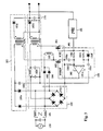
- Fig. 1 is a circuit diagram showing a construction of the first embodiment according to the present invention
- Fig. 2 is a circuit diagram depicting a construction of the second embodiment according to the present invention.
- Fig. 3 is a circuit diagram representing a construction of a modification for the second embodiment depicted in Fig. 2;
- Fig. 4 is a circuit diagram illustrating a construction of the third embodiment according to the present invention.
- Fig. 5 is a circuit diagram showing a construction of the fourth embodiment according to the present invention.
- Fig. 6 is a circuit diagram depicting another example of the turn-on timing delaying circuit provided in the converter shown in Fig. 1;
- Fig. 7 is a timing chart representing an operation of the turn-on timing delaying circuit depicted in Fig. 6;
- Fig. 8 is a circuit diagram illustrating a construction of the fifth embodiment according to the present invention.
- Fig. 1 is a circuit diagram showing a construction of the first embodiment of the AC-DC converter according to the present invention.
- the PFC power supply section and the DC-DC power supply section are connected in a parallel manner and the outputs of both the sections are added together and smoothed to be outputted.
- the AC-DC converter of the first embodiment has an AC power supply 100, an LC noise filter 101, a PFC power supply section 102, a DC-DC power supply section 103, an output adding and smoothing section 104 for adding outputs of the PFC power supply section and the DC-DC power supply section, a PWM control circuit 105, an ON time delay circuit 106, a first switching element 301 for switching the PFC power supply section and a second switching element 302 for switching the DC-DC power supply section.
- the PFC power supply section 102 comprises a bridge diode 102a, a ⁇ shaped noise filter 102b, a first transformer 102c, a rectifying diode 102d for rectifying the secondary output of the first transformer 102c.
- One end of the primary coil of the first transformer 102c is connected to the bridge diode 102a via the ⁇ shaped filter 102b and the other end of the primary coil is connected to the first switching element 301.
- the DC-DC power supply section 103 has a rectifying diodes 103a, a smoothing capacitor 103b, a second transformer 103c and a secondary rectifying diode 103d for rectifying the secondary output of the transformer 103c.
- One end of the primary coil of the second transformer 103c is connected to the smoothing capacitor 103b and the other end thereof is connected to the second switching element 302.
- the output of the PFC power supply section 102 and the output of the DC-DC power supply section 103 are added together and smoothed in the adding and smoothing section 104, then outputted to a load.
- the output of the adding and smoothing section 104 is taken out and inputted to the PWM control circuit 105 in order to conduct a servo control for operating the switching elements 301 and 302. It should be noted that only one servo control loop is provided for both the switching elements 301 and 302.
- the operation of the switching elements 301 and 302 is controlled by drive pulses PW1 and PW2 generated in the PWM control circuit 105.
- turn-on timing delaying circuit 106 is provided between the PWM control circuit 105 and the second switching element 302, so that the turn-on timing of the drive pulse PW2, which is for the second switching element, is delayed from the turn-on timing of the drive pulse PW1 for the first switching element with a given ratio. That is to say, the delay of PW2 from PW1 varies being linked with the ON time of the drive pulse PW1.
- the turn-on timing delaying circuit 106 has a comparing circuit constituted of a comparator 106a; a triangular wave generating circuit, which is provided on the plus side of the comparator 106a, being constituted of a resistor 106b, a capacitor 106c, and a diode 106d; and a averaging circuit, which is provided on the minus input side of the comparator 106a, constituted of resistors 106e and 106f, and a capacitor 106g.
- the time constant of the averaging circuit is set at a value which does not respond to the switching frequency of the second switching element 302 but responds to the commercial frequency. Therefore, the pulse width of the output PW2 of the turn-on timing delaying circuit 106 becomes smaller than that of the output PW1 of the PWM control circuit 105 with a given ratio (the duty ratio of PW2/the duty ratio of PW1).
- the first switching element 301 is driven by the output PW1 of the PWM control circuit 105 and the second switching element 302 is driven by the output PW2 of the turn-on timing delaying circuit 106, by which the turn-on timing of the PW1 is delayed from that of the PW1 with a given ratio (the duty ratio of PW2/the duty ratio of PW1); therefore, the duty ratio of the first switching element 301 becomes greater than that of the second switching element 302.
- the difference between the inductance of the first transformer 102c and the inductance of the second transformer 103c becomes shorter, compared to the case that both the transformers are switched by the switching signals driven by the signals having the same pulse width, so that the efficiency can be more improved and the size of the converter becomes more compact.
- the minus terminal of the comparator 106a may be connected to a fixed voltage. In this case, the pulse width of the output PW2 of the turn-on timing delaying circuit 106 becomes different from that of the output PW1 of the PWM control circuit 105 with a fixed difference.
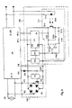
- Fig. 2 is a circuit diagram showing a construction of the second embodiment of the AC-DC converter according to the present invention. It should be noted that in the embodiments explained below the same numerical references are used for the same elements as those in the first embodiment, and the explanation for the elements is omitted here.
- a diode 201 and an inductor 202 are inserted between the bridge diode 102a and the second switching means 302 in a series manner; the other construction maintains the same condition as that of the first embodiment.
- the inductor 202 is excited, and then, when the second switching element 302 is OFF, the excited current generated in the inductor 202 is supplied to the smoothing capacitor 103b through the primary coil of the second transformer 103c, so that the capacitor 103b is charged. Therefore, the electric current coming from the rectifying circuit 103a to the smoothing capacitor 103b is reduced in the DC-DC power supply section 103, so that the generation of harmonics in the rectifying circuit 103a can be reduced.
- Fig. 3 is a circuit diagram showing a modification of the AC-DC converter mentioned in the second embodiment.
- diodes 203 and 204 and an inductor 202 are inserted between the AC inputs and the second switching element 302 in a series manner.
- harmonics can be reduced more effectively.
- Fig. 4 is a circuit diagram showing a construction of the AC-DC converter according to the third embodiment of the present invention.
- a tertiary coil 401 is provided in the first transformer 102c (or the second transformer 103c) in addition to the basic construction mentioned in Fig. 1; one of the ends of the tertiary coil 401 is connected to the smoothing circuit 103b of the DC-DC power supply section 103 and the other end thereof is connected to the noise filter 102b of the PFC power supply via a diode 402.
- the high frequency voltage generated in the switching element provided on the section where the tertiary coil 401 is provided is added to the rectified voltage so that a continuity angle of the diode402 can be made widened.
- the tertiary coil 401 is provided in the first transformer 102c of the PFC power supply section 102, however, it may be possible to provide a tertiary coil 401 in the second transformer 103c of the DC-DC power supply section 103. Further, the tertiary coil 401 is connected in a forward mode here, however it may be connected in a flyback mode.
- the other end of the tertiary coil 401 may be connected to the AC inputs.
- diodes should be inserted into both lines, respectively.
- an inductor 403 is inserted between the tertiary coil 401 and the smoothing capacitor 103b of the DC-DC power supply section 103.
- an external inductor can be also used, a leakage inductor from the tertiary coil 401 can also be used therefor.
- the rectifying diodes 103a of the DC-DC power supply section 103 can be omitted.
- the diode 201 and the inductor 202 shown in Fig. 2 and/or the diodes 203, 204 and the inductor 202 shown in Fig. 3 may be added to the third embodiment.
- the diode 201 and the diode 403 can be used commonly.
- the inductor 202 can be omitted so that only the diode is connected there.
- Fig. 5 is a circuit diagram illustrated the construction of the fourth embodiment according to the invention.
- a two -stage type AC-DC converter is shown, where the PFC power supply section 102 and the DC-DC power supply section 103 are connected together in a cascade manner.
- the PFC power supply section has a rectifying diode 102a, a ⁇ shaped filter 102b, and a choke coil 102c; to an output of the choke coil 102c, is connected the DC-DC power supply section 103 in a cascade manner, which includes a rectifying diode 103a, a smoothing capacitor 103b, a second transformer 103c, and a secondary rectifying circuit 103d.
- the output of the chock coil 102c is connected to the first switching element 301; during when the first switching element 301 is made ON, the choke coil 102c is excited; then the excited current in the choke coil 102c is stored in the smoothing capacitor 103b via the diode 103a while the first switching element 301 is OFF; then the voltage at the capacitor 103b is switched by the second switching element 302 through the primary coil of the second transformer 103c.
- a first turn-on timing delaying circuit 106-1 and a second turn-on timing delaying circuit 106-2 which operate in a linked manner, are provided between the PWM control circuit 105 and the switching elements 301 and 302, respectively.
- the first turn-on timing delaying circuit 106-1 which supplies drive pulses to the first switching element 301, has a comparing circuit constituted of a comparator 106-1a, a triangular wave generating circuit, which is provided at the plus input side of the comparator 106-1a, constituted of a resistor 106-1b, a capacitor 106-1c and a diode 106-1d, and an averaging circuit, which is provided at the minus input side of the comparator 106-1a, constituted of resistors 106-1h, 106-li and a capacitor 106-1g.
- the second turn-on timing delaying circuit 106-2 which supplies drive pulses to the second switching element 302, has a comparing circuit constituted of a comparator 106-2a, and a triangular wave generating circuit, which is provided at the plus input side of the comparator 106-2a, constituted of a resistor 106-2b, a capacitor 106-2c and a diode 106-2d; the minus input side of the comparator 106-2a is connected to a fixed voltage 106-2j.
- a voltage at smoothing capacitor 103b of the DC-DC power supply section 103 is supplied, being divided by the resistors 106-1h and 106-1i.
- the voltage at the smoothing capacitor 103b can be set at a voltage at which the best efficiency can be obtained.
- the best efficiency can be obtained, for example, at DC 260V at the smoothing capacitor 103b when the input voltage is low (100V, for instance), and at DC370V at the smoothing capacitor 103b when the input voltage is high (240V).
- the first switching element 301 is connected to the output of the choke coil 102c.
- the switching element 301 may be arranged such that the switching element 301 is connected to a tap provided in the choke coil 102c.
- the other end of the tertiary coil may be connected either to the plus side or the minus side of the noise filter 102b.
- the choke coil 102c of the PFC power supply section 102 may be substituted by a first transformer as shown by a broken line in Fig. 5. By adding a diode 102d to the first transformer, a bypass route of electric power is made there, so that efficiency can be improved.
- the manufacturing cost for the converter can be reduced because an IC for conducting a power factor correction, or a multiplier, which are required in normal two-stage type converters, are not necessary.
- another advantage can be expected that the switching noise becomes low because the switching frequency at the PFC power supply section and that at the DC-DC power supply section are the same.
- only one servo circuit is required for operating the switching elements 301 and 302; therefore, the loss can be reduced and the power consumption during standby time can be reduced.
- Fig. 6 shows a modification of the pulse width control circuit (turn-on timing delaying circuit) for the AC-DC converter according to the invention.
- the operation of the turn on timing delaying circuit 106 mentioned in the first embodiment namely, the operation for making the ON time of the second switching element 302 narrower than that of the first switching element 301 with a given ratio, is realized in another way.
- the ON time control circuit 500 comprises a current control circuit 501, a first comparator 502, a second comparator 503, an OR gate 504, a resistor 505, and a diode 506.
- the output PW1 of the PWM control circuit 105 is supplied to an input CLK of the current control circuit 501.
- the terminals ia and 4ia are connected to the minus side of the first comparator 502 and the terminals ib and 4ib are to the minus side of the second comparator 503, respectively.
- the output of the comparators 502, 503 are supplied to the OR circuit 504 and the STP terminals STPa and STPb of the current control circuit 501, respectively.
- Fig. 7 is a timing chart of the operation in the ON time control circuit 500.
- no electric current flows at any of the terminals of the current control circuit 501.
- a current flows to an output terminal ia and the voltage Vca gradually increases; during the term 2, the current at the output terminal ia stops to flow, and the voltage Vca is held.
- four times current of the current at the terminal ia flows to the terminal 4ia, so that the voltage at Vca goes down to 0V with a four times speed of that when the voltage Vca goes up during the term 1.
- the output of the first comparator 502 becomes high, so that a current stop signal is supplied to the current stop signal input terminal STPa to stop the current flow to the terminal 4ia .
- the high condition of the first comparator 502 is kept until the end of the term 4.
- a current starts up to flow to an output terminal ib and the same operation mentioned above is carried out at the output terminal ib , the second comparator 503, the input terminal 4ib and the current stop signal input terminal STPb, but with a delay from the output signal PW1 of the PWM control circuit 105 by one cycle thereof.
- the voltage at Vcb varies in the same manner as the voltage at Vca.
- the outputs OUTa and OUT b of the first and second comparators 502 and 502 are outputted alternatively as pulse signals having a delay with the rising time from that of PW1 by a given amount.
- These pulse signals are added at the OR circuit 504 to generate an output WS, which is supplied to the second switching element 302 via the resistor 505 and the diode 506.
- the output WS has the same frequency as that of the PW1 of the PWM control circuit 105, and a given LOW time corresponding to the LOW term of the output PW1 by the resistor 505 and the diode 506.
- the objected output PW2, where the ON time is narrower than that of the PW1 with a given ratio, is obtained in this manner.
- the objected pulse PW2 is generated being delayed by 1 or 2 pulses just after the control has been started up.
- the converter would have no problem by this delay at the beginning.
- the same operation in the ON time control circuit 500 can also be obtained by providing counters instead of the comparators 502 and 503. That is to say, the current control circuit 501 is arranged such that clocks having a frequency sufficiently higher than that of the PW1 are generated; the output current at the terminal ia is replaced to count-up pulses by the counter, and the current at the terminal 4ia is replaced to count-down pulses having a four times counting speed.
- the MSB outputs of the counters correspond to the outputs of the comparators 502, 503. In a case that binary counters are used, the counted-up pulse signals should be shifted by two bits and rounded off, and the count-down operation should be conducted with the same speed of the count up operation.
- the ON time of the first switching element 301 becomes 1.33 times of that of the second switching element 302.
- the pulse width changing circuit (ON time control circuit) mentioned in all of the above explained embodiments can also be realized by using a DSP (Digital Signal Processor) where the pulse widths of the two switching elements are preliminarily programmed.
- DSP Digital Signal Processor
- a flyback converter is explained; however, the present invention can also be applied to forward type converters, half bridge type converters, and full bridge type converters, etc.
- the switching element control system to be used in the converter according to the invention; that is to say, controlling systems other than a PWM system, i.e. PFM controlling system, a self- oscillating controlling system or a frequency controlling system, can be applied to the present invention.
- Fig. 8 is a block diagram showing a construction of the fifth embodiment of the AC-DC converter according to the present invention.
- the numerical reference 601 refers a power supply section including the PFC power supply section 102 and the DC-DC power supply section 103, and the first and second switching elements 301 and 302, etc.;
- the numerical reference 602 represents a driving control section of the switching elements, and 603 represents a starting-up circuit for the driving control section 602.
- the switching element driving control section 602 comprises a pulse width control circuit 611, a gate circuit 612, an oscillating circuit 613, and an intermittent oscillation control circuit 614 for controlling the operation of the pulse width control circuit 611.
- the driving control section 602 operates as follows; an output of the oscillator 613 is supplied to the pulse width control circuit 611 via the gate circuit 612 to generate the pulse outputs PW1 and PW2, then the pulse outputs PW1 and PW2 are supplied to the switching elements 301 and 302 in the power supply section 601 to obtain a DC output.
- the DC output of the power supply section 601 is taken out and returned to the control circuit 611 side via a reference voltage 614a and a photo coupler 614b; then supplied to the FB input terminal of the control circuit 611.
- the switching elements 301 and 302 oscillate intermittently.
- the intermittent frequency becomes low by the hysteresis effect of the comparator 614e, so that the strange sounds is reduced to be generated.
- a time constant circuit constituted of a capacitor 614h and a resistor 614i is provided; thereby the intermittent frequency of the switching operation can be made lower.
- the hysteresis effect is obtained by the positive feedback applied on the comparator 614e, however, it may be also obtained by a combination of two comparators and a latch circuit.
- the starting-up circuit 603 comprises a bridge diode 621, starting-up capacitors 622 and 623, which work as a reactance dropper, being provided between the bridge diode 621 and AC inputs, a voltage detecting circuit 624 provided after the bridge diode 601, a switch element 625 provided between the voltage detecting circuit 624 and one of the starting-up capacitors 623, a diode 626 connected to a VCC terminal from a VCC coil (not shown) of the power supply section 601, and a smoothing capacitor 627.
- the electric current flowing through the starting-up capacitors 621 and 622 is rectified by the bridge diode 603, then smoothed by the smoothing capacitor 627 to start up the switching element driving section 602.
- a power consumption can be reduced by using the capacitors 621 and 622 in the starting-up circuit 603 instead of a starting-up resistor.
- the smoothing capacitor 627 is so designed to suitably operate for accepting an input voltage 100V, when an input voltage 240V is applied, the voltage at the capacitor 627 becomes too high.
- the voltage detecting circuit 624 is provided in the present invention, so that when the input voltage becomes higher than a predetermined value, the switch element 625 is shortened. Thereby, when a high input voltage, for instance, 240V is applied, the current flowing the starting-up capacitor 623 becomes invalid so that the current is not stored at the smoothing capacitor 627. In this manner, the power loss, which is caused when the input voltage is high (240V) can be prevented by adding the voltage detecting circuit 624 and the switch 625.
- the voltage detecting circuit 625 It may be possible to give a hysteresis characteristic to the voltage detecting circuit 625. Further, it may also be arranged such that the power necessary to drive the control circuit 611 is obtained from the VCC terminal of the power supply section 601via the diode 627.
- the ⁇ shaped filter 102b is provided after the bridge diode 102a, however, the capacitor constituted of the filter has a very small capacitor only in comparison to that of the smoothing capacitor 103b and has almost no smoothing function. Therefore, only one capacitor may be altered therefor or both the capacitors may be omitted.
- starting-up circuit 603 and/or the switching element driving control circuit 602 can be applied to any embodiments shown in Figs. 1 to 5.
- the present invention it is arranged such that the duty ratio of the switching element of the PFC power supply section is higher than that of the switching element of the DC-DC power supply to make the inductance at the rectified current side power supply section high, so that the current waveform becomes a wide triangle shape or a trapesoidal shape. Therefore, the route-mean-square current is decreased and thus a high efficiency can be realized.
- an AC-DC converter which satisfies the IEC standard 61000-3-2 Class D without respective to the height of the input voltage, can be provided. Furthermore, a two-stage type AC-DC converter, where power consumption during standby time can be reduced and the manufacturing cost thereof can also be reduced.
Landscapes
- Engineering & Computer Science (AREA)
- Power Engineering (AREA)
- Dc-Dc Converters (AREA)
- Rectifiers (AREA)
Applications Claiming Priority (6)
| Application Number | Priority Date | Filing Date | Title |
|---|---|---|---|
| JP2000240433 | 2000-07-04 | ||
| JP2000240433 | 2000-07-04 | ||
| JP2000250341 | 2000-07-17 | ||
| JP2000250341 | 2000-07-17 | ||
| JP2001200709A JP2002101660A (ja) | 2000-07-04 | 2001-07-02 | スイッチング電源装置 |
| JP2001200709 | 2001-07-02 |
Publications (2)
| Publication Number | Publication Date |
|---|---|
| EP1170853A2 true EP1170853A2 (de) | 2002-01-09 |
| EP1170853A3 EP1170853A3 (de) | 2002-02-13 |
Family
ID=27344294
Family Applications (1)
| Application Number | Title | Priority Date | Filing Date |
|---|---|---|---|
| EP01115650A Withdrawn EP1170853A3 (de) | 2000-07-04 | 2001-07-03 | Einphasengleichstromrichter mit Leistungsfaktorregelungsfunktion |
Country Status (3)
| Country | Link |
|---|---|
| US (1) | US6388905B2 (de) |
| EP (1) | EP1170853A3 (de) |
| JP (1) | JP2002101660A (de) |
Cited By (2)
| Publication number | Priority date | Publication date | Assignee | Title |
|---|---|---|---|---|
| WO2006072917A2 (en) | 2005-01-07 | 2006-07-13 | Nxp B.V. | Switched mode power supply |
| CN104871421A (zh) * | 2012-12-21 | 2015-08-26 | 陈威伦 | 单级开关电源 |
Families Citing this family (29)
| Publication number | Priority date | Publication date | Assignee | Title |
|---|---|---|---|---|
| JP4439979B2 (ja) * | 2003-09-17 | 2010-03-24 | 太陽誘電株式会社 | 電源装置 |
| US7408795B2 (en) | 2004-02-24 | 2008-08-05 | Vlt, Inc. | Energy storage and hold-up method and apparatus for high density power conversion |
| US7561446B1 (en) | 2005-09-15 | 2009-07-14 | Vlt, Inc. | Double-clamped ZVS buck-boost power converter |
| US7548441B2 (en) * | 2004-02-24 | 2009-06-16 | Vlt, Inc. | Universal AC adapter |
| US20060028587A1 (en) * | 2004-08-05 | 2006-02-09 | Peng Juen T | TV tuner |
| JP2006187115A (ja) | 2004-12-27 | 2006-07-13 | Toshiba Corp | スイッチング電源装置及びその制御方法 |
| JP4335848B2 (ja) * | 2005-06-09 | 2009-09-30 | フジ電機工業株式会社 | オートライト制御装置 |
| US7480157B1 (en) * | 2007-11-19 | 2009-01-20 | Zippy Technology Corp. | Power architecture for providing voltage modulation power |
| JP2009296851A (ja) * | 2008-06-09 | 2009-12-17 | Sanken Electric Co Ltd | 電源装置及び電源装置の制御方法 |
| KR100938064B1 (ko) * | 2008-06-11 | 2010-01-21 | 삼성에스디아이 주식회사 | 전원 공급 장치 및 이를 구비한 플라즈마 표시 장치 |
| US20100080026A1 (en) * | 2008-10-01 | 2010-04-01 | Xiaoyang Zhang | Power factor correction circuit |
| US8698433B2 (en) * | 2009-08-10 | 2014-04-15 | Emerson Climate Technologies, Inc. | Controller and method for minimizing phase advance current |
| US8493014B2 (en) * | 2009-08-10 | 2013-07-23 | Emerson Climate Technologies, Inc. | Controller and method for estimating, managing, and diagnosing motor parameters |
| US8358098B2 (en) * | 2009-08-10 | 2013-01-22 | Emerson Climate Technologies, Inc. | System and method for power factor correction |
| US8508166B2 (en) | 2009-08-10 | 2013-08-13 | Emerson Climate Technologies, Inc. | Power factor correction with variable bus voltage |
| US8476873B2 (en) * | 2009-08-10 | 2013-07-02 | Emerson Climate Technologies, Inc. | System and method for current balancing |
| US8264192B2 (en) | 2009-08-10 | 2012-09-11 | Emerson Climate Technologies, Inc. | Controller and method for transitioning between control angles |
| DE102009037859B4 (de) * | 2009-08-18 | 2017-02-23 | Fujitsu Technology Solutions Intellectual Property Gmbh | Eingangsschaltung für ein elektrisches Gerät, Verwendung einer Eingangsschaltung und elektrisches Gerät |
| JP5304745B2 (ja) * | 2010-07-30 | 2013-10-02 | ミツミ電機株式会社 | 絶縁型電源装置および照明装置 |
| US8335096B2 (en) | 2010-11-12 | 2012-12-18 | Don Roy Sauer | Rectifier less bidirectional AC to DC converter |
| KR20130071327A (ko) * | 2011-12-20 | 2013-06-28 | 오투 마이크로, 인코포레이티드 | 복수 출력을 가진 dc/dc 컨버터 |
| US9634593B2 (en) | 2012-04-26 | 2017-04-25 | Emerson Climate Technologies, Inc. | System and method for permanent magnet motor control |
| JP6085904B2 (ja) * | 2012-05-31 | 2017-03-01 | ブラザー工業株式会社 | ノイズ低減装置、電源装置、及びノイズ低減装置におけるコアの配置方法 |
| US9240749B2 (en) | 2012-08-10 | 2016-01-19 | Emerson Climate Technologies, Inc. | Motor drive control using pulse-width modulation pulse skipping |
| KR101444371B1 (ko) * | 2013-01-18 | 2014-09-24 | (주)테라에너지시스템 | 전자기 유도 방식 전원 공급 장치 |
| CN103944421B (zh) * | 2013-01-23 | 2020-02-21 | 天宝电子(惠州)有限公司 | 电源变换器输出纹波控制电路 |
| CN103296876B (zh) * | 2013-05-31 | 2015-06-17 | 广州金升阳科技有限公司 | 一种降压式pfc的控制方法 |
| KR101459336B1 (ko) * | 2014-03-04 | 2014-11-07 | (주)테라에너지시스템 | 단위 변류기 유닛 및 이를 이용한 출력 전력을 선형적으로 조절하기 위한 전자기 유도 방식 전원 공급 장치 |
| CN109586410A (zh) * | 2018-12-10 | 2019-04-05 | 广东电网有限责任公司 | 一种电力网柜的电源滤波保护系统 |
Citations (4)
| Publication number | Priority date | Publication date | Assignee | Title |
|---|---|---|---|---|
| US5515257A (en) * | 1993-09-17 | 1996-05-07 | Toko, Inc. | AC-DC converter |
| EP0942518A2 (de) * | 1998-03-10 | 1999-09-15 | Fidelix Y.K. | Stromversorgungsvorrichtung |
| US6028776A (en) * | 1997-07-31 | 2000-02-22 | Samsung Electro-Mechanics Co. Ltd. | Power factor correction converter |
| EP0987814A1 (de) * | 1998-03-23 | 2000-03-22 | Fidelix Y.K. | Stromversorgung |
Family Cites Families (4)
| Publication number | Priority date | Publication date | Assignee | Title |
|---|---|---|---|---|
| US4338658A (en) * | 1981-05-14 | 1982-07-06 | Boschert, Incorporated | Master-slave high current D.C. power supply |
| US5351175A (en) * | 1993-02-05 | 1994-09-27 | The Lincoln Electric Company | Inverter power supply for welding |
| JP2001008452A (ja) * | 1999-06-21 | 2001-01-12 | Sony Corp | 電源装置 |
| US6201719B1 (en) * | 1999-12-22 | 2001-03-13 | Lucent Technologies Inc. | Controller for power supply and method of operation thereof |
-
2001
- 2001-07-02 JP JP2001200709A patent/JP2002101660A/ja active Pending
- 2001-07-03 US US09/898,371 patent/US6388905B2/en not_active Expired - Fee Related
- 2001-07-03 EP EP01115650A patent/EP1170853A3/de not_active Withdrawn
Patent Citations (4)
| Publication number | Priority date | Publication date | Assignee | Title |
|---|---|---|---|---|
| US5515257A (en) * | 1993-09-17 | 1996-05-07 | Toko, Inc. | AC-DC converter |
| US6028776A (en) * | 1997-07-31 | 2000-02-22 | Samsung Electro-Mechanics Co. Ltd. | Power factor correction converter |
| EP0942518A2 (de) * | 1998-03-10 | 1999-09-15 | Fidelix Y.K. | Stromversorgungsvorrichtung |
| EP0987814A1 (de) * | 1998-03-23 | 2000-03-22 | Fidelix Y.K. | Stromversorgung |
Non-Patent Citations (3)
| Title |
|---|
| BAZINET ET AL: "Monolithic controller for single stage power factor correction with isolation and soft-switching" TELECOMMUNICATIONS ENERGY CONFERENCE, 1996. INTELEC '96., 18TH INTERNATIONAL BOSTON, MA, USA 6-10 OCT. 1996, NEW YORK, NY, USA,IEEE, US, 6 October 1996 (1996-10-06), pages 248-255, XP010204326 ISBN: 0-7803-3507-4 * |
| KYU CHAN LEE CHO ET AL: "Design of the feedback loop for single controller power factor correction converter" POWER ELECTRONICS SPECIALISTS CONFERENCE, 1998. PESC 98 RECORD. 29TH ANNUAL IEEE FUKUOKA, JAPAN 17-22 MAY 1998, NEW YORK, NY, USA,IEEE, US, 17 May 1998 (1998-05-17), pages 899-904, XP010294907 ISBN: 0-7803-4489-8 * |
| YIMIN JIANG ET AL: "A NOVEL SINGLE-PHASE POWER FACTOR CORRECTION SCHEME" PROCEEDINGS OF THE ANNUAL APPLIED POWER ELECTRONICS CONFERENCE AND EXPOSITION (APEC). SAN DIEGO, MAR. 7 - 11, 1993, NEW YORK, IEEE, US, vol. CONF. 8, 7 March 1993 (1993-03-07), pages 287-292, XP000357907 ISBN: 0-7803-0983-9 * |
Cited By (6)
| Publication number | Priority date | Publication date | Assignee | Title |
|---|---|---|---|---|
| WO2006072917A2 (en) | 2005-01-07 | 2006-07-13 | Nxp B.V. | Switched mode power supply |
| WO2006072917A3 (en) * | 2005-01-07 | 2006-11-09 | Koninkl Philips Electronics Nv | Switched mode power supply |
| CN101151787B (zh) * | 2005-01-07 | 2010-10-06 | Nxp股份有限公司 | 开关式电源、用于开关式电源的控制器及其操作方法 |
| US8278900B2 (en) | 2005-01-07 | 2012-10-02 | Nxp B.V. | Switched mode power supply with burst mode controller |
| CN104871421A (zh) * | 2012-12-21 | 2015-08-26 | 陈威伦 | 单级开关电源 |
| EP2937979A4 (de) * | 2012-12-21 | 2016-10-19 | Chen Weilun | Stromquelle mit einem einpoligen schalter |
Also Published As
| Publication number | Publication date |
|---|---|
| US6388905B2 (en) | 2002-05-14 |
| EP1170853A3 (de) | 2002-02-13 |
| JP2002101660A (ja) | 2002-04-05 |
| US20020003713A1 (en) | 2002-01-10 |
Similar Documents
| Publication | Publication Date | Title |
|---|---|---|
| US6388905B2 (en) | Single phase AC-DC converter having a power factor control function | |
| EP1317052B1 (de) | Schaltnetzteil | |
| US8624572B2 (en) | Switching control circuit and switching power-supply apparatus | |
| US6307761B1 (en) | Single stage high power-factor converter | |
| CA2417771C (en) | Alexander topology resonance energy conversion and inversion circuit utilizing a series capacitance multi-voltage resonance section | |
| US7286376B2 (en) | Soft-switching power converter having power saving circuit for light load operations | |
| US5073849A (en) | Resonant DC to DC converter switching at zero current | |
| JP4924659B2 (ja) | Dc−dcコンバータ | |
| JP5544745B2 (ja) | 力率改善コンバータ | |
| US20050007088A1 (en) | Pfc-pwm controller having a power saving means | |
| EP1835606A2 (de) | Schaltnetzteilschaltung | |
| JPH07177745A (ja) | スイッチングレギュレータ | |
| CN104734510A (zh) | 开关电源及其控制芯片 | |
| US20090303751A1 (en) | Power source apparatus and control method thereof | |
| JP2011019371A (ja) | Dc−dcコンバータ | |
| US7813151B2 (en) | Variable-mode converter control circuit and half-bridge converter having the same | |
| JP2002101655A (ja) | スイッチング電源装置 | |
| JP2002300779A (ja) | スイッチング電源装置 | |
| KR20080004704A (ko) | 비씨엠모드로 동작하는 단일전력단 역률개선 회로 | |
| US20210273567A1 (en) | Switch-mode power supplies including three-level llc circuits | |
| JP2001112253A (ja) | Dc−dcコンバータ | |
| JP2004153948A (ja) | スイッチング電力電送装置 | |
| JPH1132481A (ja) | スイッチングレギュレータ | |
| KR100420964B1 (ko) | 역률보상 단일단 컨버터 | |
| JP4370844B2 (ja) | 直流変換装置 |
Legal Events
| Date | Code | Title | Description |
|---|---|---|---|
| PUAI | Public reference made under article 153(3) epc to a published international application that has entered the european phase |
Free format text: ORIGINAL CODE: 0009012 |
|
| PUAL | Search report despatched |
Free format text: ORIGINAL CODE: 0009013 |
|
| AK | Designated contracting states |
Kind code of ref document: A2 Designated state(s): AT BE CH CY DE DK ES FI FR GB GR IE IT LI LU MC NL PT SE TR |
|
| AX | Request for extension of the european patent |
Free format text: AL;LT;LV;MK;RO;SI |
|
| AK | Designated contracting states |
Kind code of ref document: A3 Designated state(s): AT BE CH CY DE DK ES FI FR GB GR IE IT LI LU MC NL PT SE TR |
|
| AX | Request for extension of the european patent |
Free format text: AL;LT;LV;MK;RO;SI |
|
| RIC1 | Information provided on ipc code assigned before grant |
Free format text: 7H 02M 3/335 A, 7H 02M 3/28 B, 7H 02M 1/12 B, 7H 02M 1/00 B |
|
| 17P | Request for examination filed |
Effective date: 20020801 |
|
| AKX | Designation fees paid |
Free format text: AT BE CH CY DE DK ES FI FR GB GR IE IT LI LU MC NL PT SE TR |
|
| STAA | Information on the status of an ep patent application or granted ep patent |
Free format text: STATUS: THE APPLICATION HAS BEEN WITHDRAWN |
|
| 18W | Application withdrawn |
Effective date: 20060620 |