EP1170603A2 - Method of fabricating silica microstructures - Google Patents
Method of fabricating silica microstructures Download PDFInfo
- Publication number
- EP1170603A2 EP1170603A2 EP01116228A EP01116228A EP1170603A2 EP 1170603 A2 EP1170603 A2 EP 1170603A2 EP 01116228 A EP01116228 A EP 01116228A EP 01116228 A EP01116228 A EP 01116228A EP 1170603 A2 EP1170603 A2 EP 1170603A2
- Authority
- EP
- European Patent Office
- Prior art keywords
- layer
- silica
- etch stop
- etching
- photoresist
- Prior art date
- Legal status (The legal status is an assumption and is not a legal conclusion. Google has not performed a legal analysis and makes no representation as to the accuracy of the status listed.)
- Withdrawn
Links
Images




Classifications
-
- H—ELECTRICITY
- H10—SEMICONDUCTOR DEVICES; ELECTRIC SOLID-STATE DEVICES NOT OTHERWISE PROVIDED FOR
- H10P—GENERIC PROCESSES OR APPARATUS FOR THE MANUFACTURE OR TREATMENT OF DEVICES COVERED BY CLASS H10
- H10P14/00—Formation of materials, e.g. in the shape of layers or pillars
- H10P14/60—Formation of materials, e.g. in the shape of layers or pillars of insulating materials
- H10P14/69—Inorganic materials
- H10P14/692—Inorganic materials composed of oxides, glassy oxides or oxide-based glasses
- H10P14/6921—Inorganic materials composed of oxides, glassy oxides or oxide-based glasses containing silicon
- H10P14/69215—Inorganic materials composed of oxides, glassy oxides or oxide-based glasses containing silicon the material being a silicon oxide, e.g. SiO2
-
- G—PHYSICS
- G02—OPTICS
- G02B—OPTICAL ELEMENTS, SYSTEMS OR APPARATUS
- G02B6/00—Light guides; Structural details of arrangements comprising light guides and other optical elements, e.g. couplings
- G02B6/10—Light guides; Structural details of arrangements comprising light guides and other optical elements, e.g. couplings of the optical waveguide type
- G02B6/12—Light guides; Structural details of arrangements comprising light guides and other optical elements, e.g. couplings of the optical waveguide type of the integrated circuit kind
- G02B6/13—Integrated optical circuits characterised by the manufacturing method
- G02B6/136—Integrated optical circuits characterised by the manufacturing method by etching
-
- H—ELECTRICITY
- H10—SEMICONDUCTOR DEVICES; ELECTRIC SOLID-STATE DEVICES NOT OTHERWISE PROVIDED FOR
- H10P—GENERIC PROCESSES OR APPARATUS FOR THE MANUFACTURE OR TREATMENT OF DEVICES COVERED BY CLASS H10
- H10P50/00—Etching of wafers, substrates or parts of devices
- H10P50/20—Dry etching; Plasma etching; Reactive-ion etching
- H10P50/28—Dry etching; Plasma etching; Reactive-ion etching of insulating materials
- H10P50/282—Dry etching; Plasma etching; Reactive-ion etching of insulating materials of inorganic materials
- H10P50/283—Dry etching; Plasma etching; Reactive-ion etching of insulating materials of inorganic materials by chemical means
-
- H—ELECTRICITY
- H10—SEMICONDUCTOR DEVICES; ELECTRIC SOLID-STATE DEVICES NOT OTHERWISE PROVIDED FOR
- H10P—GENERIC PROCESSES OR APPARATUS FOR THE MANUFACTURE OR TREATMENT OF DEVICES COVERED BY CLASS H10
- H10P50/00—Etching of wafers, substrates or parts of devices
- H10P50/73—Etching of wafers, substrates or parts of devices using masks for insulating materials
-
- G—PHYSICS
- G02—OPTICS
- G02B—OPTICAL ELEMENTS, SYSTEMS OR APPARATUS
- G02B6/00—Light guides; Structural details of arrangements comprising light guides and other optical elements, e.g. couplings
- G02B6/10—Light guides; Structural details of arrangements comprising light guides and other optical elements, e.g. couplings of the optical waveguide type
- G02B6/12—Light guides; Structural details of arrangements comprising light guides and other optical elements, e.g. couplings of the optical waveguide type of the integrated circuit kind
- G02B2006/12035—Materials
- G02B2006/12038—Glass (SiO2 based materials)
Definitions
- the present invention relates generally to integrated optical devices, and in particular, to a method of fabricating silica microstructures.
- Integrated optics technology has continuously been developed.
- the integrated optics is characterized by small size, low price, low power, and high speed as compared to assembly of individual optical parts.
- PLC planar lightwave circuit
- MEMS micro-electromechanical system
- the PLC refers to a device with a waveguide formed of silica being a fiber material on a silicon substrate. It is known that an existing fiber optic-type splitter is superior to a PLC splitter at a split ratio up to 1x4 but vice versa at a higher split ratio. The PLC realizes a compact and mass-produced circuit and provides excellent cost performance.
- MEMS emerged from silicon processing technology and primitive MEMS applications include valves, motors, pumps, gears, and the like that are formed two-dimensionally. Integration of micro devices through anisotropical etching of a semiconductor substrate was studied and three-dimensional fiber optic devices have been developed. The recently developed technology in this field is about fabrication of three-dimensional thin film structures by etching a sacrificial thin film on a semiconductor substrate.
- silica layer It is necessary to etch a silica layer to a specific depth in fabrication of silica microstructures such as PLC and MEMS devices.
- integrated devices must be arranged perpendicularly to a silica light waveguide in fabricating a silica PLC in a hybrid integration scheme.
- the overcladding layer of the silica light waveguide must be removed from its core layer to a predetermined depth.
- the overcladding layer is formed on the core layer with a thickness deviation of 7 ⁇ m or greater, the thickness of the overcladding layer cannot be known accurately. Therefore, it is very difficult to etch the overcladding layer to the predetermined depth.
- the object of the present invention to provide a silica microstructures fabrication method for stopping etching at a desired position during a dry etch.
- the foregoing object can be achieved by providing a silica microstructure fabrication method.
- An etch stop layer is first partially deposited on an etching area of a first silica layer formed on a semiconductor substrate.
- a second silica layer is deposited on the surfaces of the etch stop layer and the first silica layer.
- a mask patterned according to the shape of the etching area is formed on the surface of the second silica layer.
- the second silica layer is removed from the etching area using the mask by dry etching, and the etch stop layer is removed by wet etching.
- FIGs. 1A to 4 are sectional views sequentially illustrating a silica microstructures fabrication method according to a preferred embodiment of the present invention.
- FIG. 1A illustrates the step of depositing a first silica layer 12 on a silicon substrate 11.
- the first silica layer 12 is formed by deposition like flame hydrolysis deposition, APCVD (Atmospheric Pressure Chemical Vapor Deposition), PACVD (Plasma Enhanced CVD), and thermal oxidation.
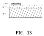
- FIG. 1B illustrates the step of partially depositing an etch stop layer 113 on an etching area of the first silica layer 12.
- the etch stop layer 13 is partially deposited by loft-off or etching.
- a photoresist layer is deposited on the first silica layer 12 and patterned according to the shape of the etching area. Then, an etch stop layer is formed on the photoresist layer and the first silica layer 12 by e-beams or sputtering and the photoresist layer is removed along with the etch stop layer formed on the photoresist layer using a photoresist remover like acetone.
- an etch stop layer is first formed on the first silica layer 12 by e-beams or sputtering and a photoresist layer is formed on the etch stop layer and patterned according to the shape of the etching area. Then, the etch stop layer is dry-etched using the photoresist pattern. RIE (Reactive Ion Etching) can be used for the dry etching of the etch stop layer.
- the etch stop layer 13 must be formed of a material having a high etch selectivity with respect to silica and resistant against oxidation or corrosion during silica deposition. Such materials include gold and platinum, which may incur clustering due to surface tension if silica deposition at high temperature such as flame hydrolysis deposition is applied. Ceramic materials for the etch stop layer 13 include alumina tolerant at high temperature and showing a high etch selectivity.
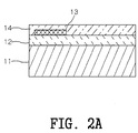
- FIG. 2A illustrates the step of a second silica layer 14 on the overall surface of the resultant structure including the etch stop layer 13 and the first silica layer 12.
- the second silica layer 14 can be formed in the same manner as the first silica layer 12, that is, by deposition.
- FIG. 2B illustrates the step of forming a mask 15 patterned according to the shape of the etching area on the second silica layer 14.
- the mask 15 is preferably formed of a metal.
- a metal mask is usually used to etch a layer too thick to be etched using a photoresist.
- a general metal mask formation method includes the steps of forming a metal layer, forming a photoresist layer on the metal layer, patterning the photoresist layer, and etching the metal layer using the photoresist pattern.
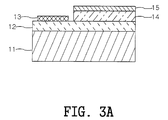
- FIG. 3A illustrates the step of removing the second silica layer 14 from the etching area using the mask 15 by dry etching.
- a silica layer is etched typically by dry etching or wet etching. Wet etching is so called because an object is etched in a liquid such as an acid, an alkali, or an organic solvent. Dry etching includes RIE and inductively coupled plasma etching using plasma etching equipment. Anisotropical etching is difficult and formation of a vertical side profile is impossible in wet etching, whereas an etch speed is easily controlled and a vertical side profile can be obtained in dry etching.
- FIG. 3B illustrates the step of removing the mask from the surface of the second silica layer 14.
- the mask 15 is removed using an appropriate etchant according to the material of the mask 15. For example, if the mask 15 is a photoresist, a photoresist remover is used. If the mask 15 is formed of chrome, a chrome remover is used.
- FIG. 4 illustrate the step of removing the etch stop layer 13. It is convenient in the processing aspect to remove the etch stop layer 13 by wet etching. Usual chemical solutions for wet etching are H 2 SO 4 , H 3 PO 4 , H 2 O 2 , HF, HCL, and NH 4 OH.
- the silica microstructure fabrication method according to the present invention is advantage in that etching can be stopped at a desired position using an etch stop layer in dry-etching a silica layer.
Landscapes
- Physics & Mathematics (AREA)
- Engineering & Computer Science (AREA)
- Microelectronics & Electronic Packaging (AREA)
- General Physics & Mathematics (AREA)
- Optics & Photonics (AREA)
- Drying Of Semiconductors (AREA)
- Optical Integrated Circuits (AREA)
- Micromachines (AREA)
- Photosensitive Polymer And Photoresist Processing (AREA)
- Weting (AREA)
Abstract
Description
Claims (8)
- A silica microstructure fabrication method comprising the steps of:partially depositing an etch stop layer on an etching area of a first silica layer formed on a semiconductor substrate;forming a second silica layer on the surfaces of the etch stop layer and the first silica layer;forming a mask patterned according to the shape of the etching area on the surface of the second silica layer;removing the second silica layer from the etching area using the mask by dry etching; andremoving the etch stop layer by wet etching.
- The silica microstructure fabrication method of claim 1, wherein the etch stop layer deposition step comprises the steps of:depositing a photoresist layer on the first silica layer;patterning the photoresist layer according to the shape of the etching area;forming the etch stop layer on the surfaces of the photoresist layer and the first silica layer; andremoving the photoresist layer using a photoresist remover.
- The silica microstructure fabrication method of claim 1, wherein the etch stop layer deposition step comprises the steps of:forming the etch stop layer on the first silica layer;forming a photoresist layer on the etch stop layer;patterning the photoresist layer according to the shape of the etching area; anddry-etching the etch stop layer using the photoresist pattern.
- The silica microstructure fabrication method of one of the claims 1-3, wherein the etch stop layer is formed of one of metal and ceramic.
- The silica microstructure fabrication method of claim 1, wherein the mask formation step comprises the steps of:forming a metal layer on the second silica layer by sputtering;forming a photoresist layer on the metal layer;patterning the photoresist layer according to the shape of the etching area; andetching the metal layer using the photoresist pattern.
- The silica microstructure fabrication method of claim 1, wherein the first and second silica layers are formed by deposition.
- The silica microstructure fabrication method of claim 1, wherein the second silica layer is dry-etched by Reactive Ion Etching (RIE).
- A silica microstructure that is fabricated according to the method of any one of the claims 1-7.
Applications Claiming Priority (2)
| Application Number | Priority Date | Filing Date | Title |
|---|---|---|---|
| KR2000038692 | 2000-07-06 | ||
| KR1020000038692A KR100326317B1 (en) | 2000-07-06 | 2000-07-06 | Fabrication method of silica microstructures |
Publications (2)
| Publication Number | Publication Date |
|---|---|
| EP1170603A2 true EP1170603A2 (en) | 2002-01-09 |
| EP1170603A3 EP1170603A3 (en) | 2004-06-16 |
Family
ID=19676670
Family Applications (1)
| Application Number | Title | Priority Date | Filing Date |
|---|---|---|---|
| EP01116228A Withdrawn EP1170603A3 (en) | 2000-07-06 | 2001-07-04 | Method of fabricating silica microstructures |
Country Status (4)
| Country | Link |
|---|---|
| US (1) | US6756319B2 (en) |
| EP (1) | EP1170603A3 (en) |
| JP (1) | JP3421016B2 (en) |
| KR (1) | KR100326317B1 (en) |
Families Citing this family (7)
| Publication number | Priority date | Publication date | Assignee | Title |
|---|---|---|---|---|
| KR100326317B1 (en) * | 2000-07-06 | 2002-03-08 | 윤종용 | Fabrication method of silica microstructures |
| KR100480030B1 (en) * | 2002-10-24 | 2005-03-31 | 엘지전자 주식회사 | Manufacturing method of thin film bulk acoustic resonator and filter |
| US7372689B2 (en) * | 2005-04-04 | 2008-05-13 | International Business Machines Corporation | Guard wafer for semiconductor structure fabrication |
| US7667242B1 (en) | 2006-10-23 | 2010-02-23 | Northrop Grumman Systems Corporation | Systems and methods for maximizing breakdown voltage in semiconductor devices |
| US7557046B1 (en) * | 2006-10-23 | 2009-07-07 | Northrop Grumman Systems Corporation | Systems and methods for interconnect metallization using a stop-etch layer |
| KR100855406B1 (en) * | 2007-12-27 | 2008-08-29 | 주식회사 동부하이텍 | Image sensor manufacturing method |
| JP2020098283A (en) * | 2018-12-18 | 2020-06-25 | 日本電信電話株式会社 | Optical waveguide and manufacturing method of the same |
Family Cites Families (20)
| Publication number | Priority date | Publication date | Assignee | Title |
|---|---|---|---|---|
| JP2581089B2 (en) | 1987-07-24 | 1997-02-12 | ブラザー工業株式会社 | Method for manufacturing optical integrated circuit having mask |
| JPH04313710A (en) | 1990-03-14 | 1992-11-05 | Fujitsu Ltd | Production of optical waveguide parts |
| US5284549A (en) * | 1992-01-02 | 1994-02-08 | International Business Machines Corporation | Selective fluorocarbon-based RIE process utilizing a nitrogen additive |
| ATE269588T1 (en) * | 1993-02-04 | 2004-07-15 | Cornell Res Foundation Inc | MICROSTRUCTURES AND SINGLE MASK, SINGLE CRYSTAL PRODUCTION PROCESS |
| US5330920A (en) * | 1993-06-15 | 1994-07-19 | Digital Equipment Corporation | Method of controlling gate oxide thickness in the fabrication of semiconductor devices |
| JPH07241690A (en) | 1994-03-07 | 1995-09-19 | Hitachi Ltd | Dielectric mask for laser processing and manufacturing method thereof |
| JPH07283215A (en) | 1994-04-08 | 1995-10-27 | Sharp Corp | Method for manufacturing optical integrated circuit |
| FR2749672B1 (en) * | 1996-06-06 | 1998-07-03 | Commissariat Energie Atomique | VERTICAL POSITIONING OF AN OPTOELECTRONIC COMPONENT ON A SUPPORT, WITH REGARD TO AN OPTICAL GUIDE INTEGRATED IN THIS SUPPORT |
| JPH10268526A (en) | 1997-03-24 | 1998-10-09 | Toshiba Corp | Semiconductor device manufacturing method and pattern forming method |
| US6051510A (en) * | 1997-05-02 | 2000-04-18 | Advanced Micro Devices, Inc. | Method of using a hard mask to grow dielectrics with varying characteristics |
| KR19990012248A (en) | 1997-07-28 | 1999-02-25 | 윤종용 | Manufacturing method of optical waveguide device |
| TW343364B (en) * | 1997-09-26 | 1998-10-21 | United Microelectronics Corp | Process for producing twin gate oxide elements |
| JPH11204414A (en) | 1998-01-19 | 1999-07-30 | Nippon Telegr & Teleph Corp <Ntt> | Pattern formation method |
| US6340435B1 (en) * | 1998-02-11 | 2002-01-22 | Applied Materials, Inc. | Integrated low K dielectrics and etch stops |
| US6268287B1 (en) * | 1999-10-15 | 2001-07-31 | Taiwan Semiconductor Manufacturing Company | Polymerless metal hard mask etching |
| US6262455B1 (en) * | 1999-11-02 | 2001-07-17 | Philips Semiconductor, Inc. | Method of forming dual gate oxide layers of varying thickness on a single substrate |
| US6376156B1 (en) * | 1999-11-22 | 2002-04-23 | Taiwan Semiconductor Manufacturing Company | Prevent defocus issue on wafer with tungsten coating on back-side |
| US6306706B1 (en) * | 2000-03-30 | 2001-10-23 | Advanced Micro Devices, Inc. | Method and system for fabricating a flash memory array |
| US20020031711A1 (en) * | 2000-05-09 | 2002-03-14 | Steinberg Dan A. | Multi-level lithography masks |
| KR100326317B1 (en) * | 2000-07-06 | 2002-03-08 | 윤종용 | Fabrication method of silica microstructures |
-
2000
- 2000-07-06 KR KR1020000038692A patent/KR100326317B1/en not_active Expired - Fee Related
-
2001
- 2001-06-29 JP JP2001198700A patent/JP3421016B2/en not_active Expired - Fee Related
- 2001-07-04 EP EP01116228A patent/EP1170603A3/en not_active Withdrawn
- 2001-07-05 US US09/899,784 patent/US6756319B2/en not_active Expired - Lifetime
Also Published As
| Publication number | Publication date |
|---|---|
| JP3421016B2 (en) | 2003-06-30 |
| KR100326317B1 (en) | 2002-03-08 |
| US20020004316A1 (en) | 2002-01-10 |
| KR20020004627A (en) | 2002-01-16 |
| JP2002156745A (en) | 2002-05-31 |
| EP1170603A3 (en) | 2004-06-16 |
| US6756319B2 (en) | 2004-06-29 |
Similar Documents
| Publication | Publication Date | Title |
|---|---|---|
| US6946238B2 (en) | Process for fabrication of optical waveguides | |
| US20070177287A1 (en) | Method of manufacturing a mirror and a mirror device | |
| US6627096B2 (en) | Single mask technique for making positive and negative micromachined features on a substrate | |
| US7016587B2 (en) | Low loss silicon waveguide and method of fabrication thereof | |
| EP1170603A2 (en) | Method of fabricating silica microstructures | |
| KR20090010930A (en) | Boron Doped Shell for MEMS Devices | |
| Lee et al. | Vertical mirror fabrication combining KOH etch and DRIE of (110) silicon | |
| KR20070045204A (en) | Method for manufacturing optical waveguide assembly with integral alignment features | |
| JP3890046B2 (en) | Method for manufacturing planar circuit type optical element | |
| Moosburger et al. | Passive alignment of single-mode fibers to integrated polymer waveguide structures utilizing a single-mask process | |
| WO2006136194A1 (en) | Method for fabricating a turning mirror for optical devices | |
| US6613243B2 (en) | Method of making a 3-D structure using an erodable mask formed from a film having a composition that varies in its direction of thickness | |
| WO2001057566A2 (en) | Buried high precision alignemnt marks for optical waveguides with thick overcladding | |
| US6483964B1 (en) | Method of fabricating an optical component | |
| EP4320479B1 (en) | Light source, mems optical switch, sensor and methods for manufacturing the same | |
| US6510275B1 (en) | Micro-optoelectromechanical system based device with aligned structures and method for fabricating same | |
| Pandraud et al. | Micromachining of high-contrast optical waveguides in [111] silicon wafers | |
| JP4994096B2 (en) | Semiconductor device manufacturing method and semiconductor device using the same | |
| EP1174763A2 (en) | Method of fabricating a nickel etching mask | |
| CA2349031A1 (en) | Method of fabricating mode-size converter with three dimensional tapered with high processing tolerance | |
| Butt et al. | Fabrication of silicon slanted grating by using modified thermal deposition technique to enhance fiber-to-chip coupling | |
| KR20040036759A (en) | FABRICATION METHOD FOR PLANAR LIGHTWAVEGUIDE USING OF Si ETCHING | |
| JPH07318740A (en) | Method of manufacturing optical waveguide having reflective portion | |
| Cristea et al. | Silicon waveguide fabrication process based on the anisotropic etching of Si< 111>-oriented wafers | |
| JPH10239541A (en) | Optical waveguide and manufacture thereof |
Legal Events
| Date | Code | Title | Description |
|---|---|---|---|
| PUAI | Public reference made under article 153(3) epc to a published international application that has entered the european phase |
Free format text: ORIGINAL CODE: 0009012 |
|
| 17P | Request for examination filed |
Effective date: 20010704 |
|
| AK | Designated contracting states |
Kind code of ref document: A2 Designated state(s): AT BE CH CY DE DK ES FI FR GB GR IE IT LI LU MC NL PT SE TR |
|
| AX | Request for extension of the european patent |
Free format text: AL;LT;LV;MK;RO;SI |
|
| PUAL | Search report despatched |
Free format text: ORIGINAL CODE: 0009013 |
|
| AK | Designated contracting states |
Kind code of ref document: A3 Designated state(s): AT BE CH CY DE DK ES FI FR GB GR IE IT LI LU MC NL PT SE TR |
|
| AX | Request for extension of the european patent |
Extension state: AL LT LV MK RO SI |
|
| RIC1 | Information provided on ipc code assigned before grant |
Ipc: 7G 02B 6/12 B Ipc: 7G 02B 6/36 A |
|
| AKX | Designation fees paid |
Designated state(s): DE FR GB |
|
| STAA | Information on the status of an ep patent application or granted ep patent |
Free format text: STATUS: THE APPLICATION IS DEEMED TO BE WITHDRAWN |
|
| 18D | Application deemed to be withdrawn |
Effective date: 20061013 |