EP1168604A1 - Multistage amplifier - Google Patents
Multistage amplifier Download PDFInfo
- Publication number
- EP1168604A1 EP1168604A1 EP00902144A EP00902144A EP1168604A1 EP 1168604 A1 EP1168604 A1 EP 1168604A1 EP 00902144 A EP00902144 A EP 00902144A EP 00902144 A EP00902144 A EP 00902144A EP 1168604 A1 EP1168604 A1 EP 1168604A1
- Authority
- EP
- European Patent Office
- Prior art keywords
- stage
- amplifying element
- impedance
- pass filter
- filter type
- Prior art date
- Legal status (The legal status is an assumption and is not a legal conclusion. Google has not performed a legal analysis and makes no representation as to the accuracy of the status listed.)
- Withdrawn
Links
Images





Classifications
-
- H—ELECTRICITY
- H03—ELECTRONIC CIRCUITRY
- H03F—AMPLIFIERS
- H03F3/00—Amplifiers with only discharge tubes or only semiconductor devices as amplifying elements
- H03F3/60—Amplifiers in which coupling networks have distributed constants, e.g. with waveguide resonators
- H03F3/602—Combinations of several amplifiers
-
- H—ELECTRICITY
- H03—ELECTRONIC CIRCUITRY
- H03F—AMPLIFIERS
- H03F1/00—Details of amplifiers with only discharge tubes, only semiconductor devices or only unspecified devices as amplifying elements
- H03F1/56—Modifications of input or output impedances, not otherwise provided for
- H03F1/565—Modifications of input or output impedances, not otherwise provided for using inductive elements
-
- H—ELECTRICITY
- H03—ELECTRONIC CIRCUITRY
- H03H—IMPEDANCE NETWORKS, e.g. RESONANT CIRCUITS; RESONATORS
- H03H7/00—Multiple-port networks comprising only passive electrical elements as network components
- H03H7/38—Impedance-matching networks
-
- H—ELECTRICITY
- H03—ELECTRONIC CIRCUITRY
- H03F—AMPLIFIERS
- H03F2200/00—Indexing scheme relating to amplifiers
- H03F2200/318—A matching circuit being used as coupling element between two amplifying stages
-
- H—ELECTRICITY
- H03—ELECTRONIC CIRCUITRY
- H03F—AMPLIFIERS
- H03F2201/00—Indexing scheme relating to details of amplifiers with only discharge tubes, only semiconductor devices or only unspecified devices as amplifying elements covered by H03F1/00
- H03F2201/32—Indexing scheme relating to modifications of amplifiers to reduce non-linear distortion
- H03F2201/3215—To increase the output power or efficiency
Definitions
- the present invention relates to a multistage amplifier in which an input signal is amplified stage by stage and is output.
- an input matching circuit placed on an input side In a multistage amplifier using a type of semiconductor devices such as field effect transistors (FETs), bipolar junction transistors (BJTs) or hetero junction bipolar transistors (HBTs), an input matching circuit placed on an input side, an output matching circuit placed on an output side and an inter-stage matching circuit placed between the input matching circuit and the output matching circuit are generally arranged so as to bring out the performance of the type of semiconductor devices.
- FETs field effect transistors
- BJTs bipolar junction transistors
- HBTs hetero junction bipolar transistors
- Fig. 1 is a view of an equivalent circuit of a conventional multistage amplifier disclosed in "Technical Report of the Institute of Electronics, Information and Communication Engineers (IEICE), MW95-73", published in July of 1995.
- IEICE Institute of Electronics, Information and Communication Engineers
- 1 indicates an input terminal for receiving a signal.
- 2 indicates an output terminal for outputting an amplified signal.
- 3 indicates a front-stage amplifying element for amplifying the signal received in the input terminal 1.
- 4 indicates a rear-stage amplifying element for amplifying the signal amplified in the front-stage amplifying element 3.
- 5 indicates an input matching circuit of the conventional multistage amplifier.
- 6 indicates an inter-stage matching circuit for performing an impedance matching between the front-stage amplifying element 3 and the rear-stage amplifying element 4.
- 7 indicates a bias circuit.
- 8 indicates an output matching circuit of the conventional multistage amplifier.
- 9 indicates a short stub for bias supply.
- 10 indicates a parallel capacitor.
- 11 indicates a serial line.
- 12 indicates a serial capacitor.
- each of the front-stage amplifying element 3 and the rear-stage amplifying element 4 is composed of an FET, a BJT, a metal oxide semiconductor field effect transistor (MOSFET), a high electron mobility transistor (HEMT) or an HBT.
- MOSFET metal oxide semiconductor field effect transistor
- HEMT high electron mobility transistor
- the signal When a signal is received in the input terminal 1, the signal is sent to the front-stage amplifying element 3 through the input matching circuit 5, and the signal is amplified in the front-stage amplifying element 3.
- the signal amplified in the front-stage amplifying element 3 is sent to the rear-stage amplifying element 4 through the inter-stage matching circuit 6 and the bias circuit 7, and the signal is amplified in the rear-stage amplifying element 4.
- the signal amplified in the rear-stage amplifying element 4 is output from the output terminal 2 through the output matching circuit 8.
- Fig. 2 is an explanatory view showing a general example of matching conditions between the front-stage amplifying element 3 and the rear-stage amplifying element 4 of the conventional multistage amplifier.
- an output impedance of the front-stage amplifying element 3 is expressed by S Y_FET
- an impedance (that is, an output load impedance of the front-stage amplifying element 3) on an output side seen from the front-stage amplifying element 3 is expressed by F out
- an input impedance of the rear-stage amplifying element 4 is expressed by S x_FET
- an impedance (that is, an input source impedance of the rear-stage amplifying element 4) on an input side seen from the rear-stage amplifying element 4 is expressed by F in .
- an optimum output load impedance ⁇ opt_out of the front-stage amplifying element 3 agrees with a conjugate complex impedance S Y_FET * of the output impedance S Y_FET of the front-stage amplifying element 3
- an optimum input source impedance ⁇ opt_in of the rear-stage amplifying element 4 agrees with a conjugate complex impedance S X_FET * of the input impedance S X_FET of the rear-stage amplifying element 4.
- the conjugate complex impedance matching can be performed at the input terminal Y of the rear-stage amplifying element 4 simultaneously with the conjugate complex impedance matching at the output terminal X.
- a level of the input signal transmitted through the multistage amplifier induces the conventional multistage amplifier to perform a large signal operation in a final-stage amplifying element or an amplifying element just before the final-stage amplifying element of the conventional multistage amplifier in place of the small signal operation.
- the output impedance S Y_FET of the front-stage amplifying element 3 and the input impedance S X_FET of the rear-stage amplifying element 4 in the large signal operation of the conventional multistage amplifier differ from those in the small signal operation, and optimum impedances, which maximize an efficiency of the conventional multistage amplifier, differ from the input and output impedances S X_FET and S Y_FET .
- the optimum output load impedance ⁇ opt_out of the front-stage amplifying element 3 differs from the conjugate complex impedance S Y_FET * of the output impedance S Y_FET of the front-stage amplifying element 3, and the optimum input source impedance ⁇ opt_in of the rear-stage amplifying element 4 differs from the conjugate complex impedance S X_FET * of the input impedance S X_FET of the rear-stage amplifying element 4.
- the inter-stage matching circuit 6 is designed so as to perform an impedance transformation from the input impedance S X_FET of the rear-stage amplifying element 4 to the optimum output load impedance ⁇ opt_out ( ⁇ S Y_FET *) of the front-stage amplifying element 3. Also, in cases where a conjugate complex impedance matching is performed at the input terminal Y of the rear-stage amplifying element 4, as shown in Fig.
- the inter-stage matching circuit 6 is designed so as to perform an impedance transformation from the output impedance S Y_FET of the front-stage amplifying element 3 to the optimum input source impedance ⁇ opt_in ( ⁇ S X_FET *) of the rear-stage amplifying element 4.
- the inter-stage matching circuit 6 it is impossible for the inter-stage matching circuit 6 to perform the conjugate complex impedance matching at the output terminal X of the front-stage amplifying element 3 simultaneously with the conjugate complex impedance matching at the input terminal Y of the rear-stage amplifying element 4.
- the conventional multistage amplifier has the above described configuration, it is impossible to perform the matching of the output load impedance F out of the front-stage amplifying element 3 with the optimum output load impedance ⁇ opt_out simultaneously with the matching of the input source impedance F in of the rear-stage amplifying element 4 with the optimum input source impedance ⁇ opt_in . Therefore, a problem has arisen that an efficiency of the whole conventional multistage amplifier is lowered.
- the present invention is provided to solve the above-described problem, and the object of the present invention is to provide a multistage amplifier in which an output load impedance of a front-stage amplifying element and an input source impedance of a rear-stage amplifying element are simultaneously matched with optimum impedances respectively.
- a multistage amplifier according to the present invention has a matching circuit comprising a one-stage high pass filter type matching unit and a one-stage low pass filter type matching unit serially connected with the one-stage high pass filter type matching unit.
- an output load impedance of a front-stage amplifying element and an input source impedance of a rear-stage amplifying element can be matched with the optimum impedances respectively, an efficiency of the whole multistage amplifier can be heightened.
- the matching circuit arranged between the final-stage amplifying element and the amplifying element placed just before the final-stage amplifying element comprises the one-stage high pass filter type matching unit and the one-stage low pass filter type matching unit serially connected with each other.
- the one-stage high pass filter type matching unit is placed on an input side of the input signal, and the one-stage low pass filter type matching unit is placed on an output side of the amplified signal.
- an output load impedance of a front-stage amplifying element and an input source impedance of a rear-stage amplifying element can be matched with the optimum impedances respectively.
- the one-stage low pass filter type matching unit is placed on an input side of the input signal, and the one-stage high pass filter type matching unit is placed on an output side of the amplified signal.
- an output load impedance of a front-stage amplifying element and an input source impedance of a rear-stage amplifying element can be matched with the optimum impedances respectively.
- the one-stage high pass filter type matching unit comprises a parallel inductor and a serial capacitor.
- a bias supply short stub having a length equal to or shorter than 1/4 of a wavelength of the input signal is used as the parallel inductor.
- the bias supply short stub can be used as a bias supply line on an output side of the front-stage amplifying element, a small-sized multistage amplifier can be obtained.
- the one-stage low pass filter type matching unit comprises a parallel capacitor and a serial inductor.
- a serial line is used as the serial inductor.
- Fig. 3 is a view of an equivalent circuit of a multistage amplifier according to a first embodiment of the present invention.
- 21 indicates an input terminal for receiving a signal.
- 22 indicates an output terminal for outputting an amplified signal.
- 23 indicates a front-stage amplifying element for amplifying the signal received in the input terminal 21.
- 24 indicates a rear-stage amplifying element for amplifying the signal amplified in the front-stage amplifying element 23.
- 25 indicates an input matching circuit of the multistage amplifier.
- 26 indicates an inter-stage matching circuit for performing an impedance matching between the front-stage amplifying element 23 and the rear-stage amplifying element 24.
- 27 indicates an output matching circuit of the multistage amplifier.
- 28 indicates a one-stage high pass filter type matching unit of the inter-stage matching circuit 26.
- 29 indicates a one-stage low pass filter type matching unit of the inter-stage matching circuit 26.
- 31 indicates a parallel inductor of the one-stage high pass filter type matching unit 28.
- 32 indicates a serial capacitor of the one-stage high pass filter type matching unit 28.
- 33 indicates a parallel capacitor of the one-stage low pass filter type matching unit 29.
- 34 indicates a serial inductor of the one-stage low pass filter type matching unit 29.
- each of the front-stage amplifying element 23 and the rear-stage amplifying element 24 is composed of an FET, a BJT, an MOSFET, an HEMT or an HBT.
- the signal When a signal is received in the input terminal 21, the signal is sent to the front-stage amplifying element 23 through the input matching circuit 25, and the signal is amplified in the front-stage amplifying element 23.
- the signal amplified in the front-stage amplifying element 23 is sent to the rear-stage amplifying element 24 through the inter-stage matching circuit 26 comprising the one-stage high pass filter type matching unit 28 and the one-stage low pass filter type matching unit 29, and the signal is amplified in the rear-stage amplifying element 24.
- the signal amplified in the rear-stage amplifying element 24 is output from the output terminal 22 through the output matching circuit 27.
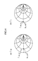
- a high electron mobility transistor (HEMT) element having a gate width of 5.8 mm is, for example, used as the front-stage amplifying element 23, an optimum output load impedance ⁇ opt_out of the HEMT element and a conjugate complex impedance S Y_FET * of an output impedance of the HEMT element are shown in Fig. 4(a).
- HEMT high electron mobility transistor
- a high electron mobility transistor (HEMT) element having a gate width of 17.5 mm is, for example, used as the rear-stage amplifying element 24, an optimum input source impedance ⁇ opt_in of the HEMT element and a conjugate complex impedance S X_FET * of an input impedance of the HEMT element are shown in Fig. 4(b).
- HEMT high electron mobility transistor
- Bias conditions for the HEMT elements are Class-AB together.
- the gate width of the front-stage amplifying element 23 is equal to or lower than a half of the gate width of the rear-stage amplifying element 24.
- the optimum input source impedance ⁇ opt_in of the rear-stage amplifying element 24 corresponds to an impedance, at which a maximum efficiency is obtained in the multistage amplifier, in cases where a prescribed distortion condition is satisfied at an output electric power level of almost 3 dB in back off, and the optimum input source impedance ⁇ opt_in is determined by performing load-pull and source-pull measurements.
- the optimum output load impedance ⁇ opt_out of the front-stage amplifying element 23 (the HEMT element of the gate width of 5.8 mm) is determined by examining various combinations of characteristics of the front-stage amplifying element 23 and the rear-stage amplifying element 24 according to both a result of load-pull and source-pull measurements for the HEMT element of the gate width of 5.8 mm and the result of the load-pull and source-pull measurements for the HEMT element of the gate width of 17.5 mm, determining a specific combination of characteristics of the front-stage amplifying element 23 and the rear-stage amplifying element 24 on condition that a maximum efficiency in the multistage amplifier is obtained in cases where a prescribed distortion condition is satisfied as a two-stage amplifier at an output electric power level of almost 3 dB in back off and adopting an output load impedance of the front-stage amplifying element 23 determined in the specific combination as the optimum output load impedance ⁇ opt_out .
- a real part of the optimum output load impedance ⁇ opt_out of the front-stage amplifying element 23 (the HEMT element of the gate width of 5.8 mm) is moved toward a low impedance direction as compared with the conjugate complex impedance S Y_FET * of the output impedance of the front-stage amplifying element 23, and an imaginary part of the optimum output load impedance ⁇ opt_out of the front-stage amplifying element 23 is moved toward an inductive direction as compared with the conjugate complex impedance S Y_FET * of the output impedance of the front-stage amplifying element 23.
- a real part of the optimum input source impedance ⁇ opt_in of the rear-stage amplifying element 24 (the HEMT element of the gate width of 17.5 mm) is moved toward a high impedance direction as compared with the conjugate complex impedance S X_FET * of the input impedance of the rear-stage amplifying element 24, and an imaginary part of the optimum input source impedance ⁇ opt_in of the rear-stage amplifying element 24 is moved toward an inductive direction as compared with the conjugate complex impedance S X_FET * of the input impedance of the rear-stage amplifying element 24.
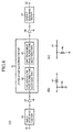
- an output load impedance ⁇ out of the front-stage amplifying element 23 and an input source impedance ⁇ in of the rear-stage amplifying element 24 are shown in Fig. 5 in cases where the inter-stage matching circuit 26 comprising the one-stage high pass filter type matching unit 28 and the one-stage low pass filter type matching unit 29 is used for the multistage amplifier.
- impedances designated by symbols ⁇ indicate the conjugate complex impedance S Y_FET * of the output impedance of the front-stage amplifying element 23 and the conjugate complex impedance S X_FET * of the input impedance of the rear-stage amplifying element 24 respectively
- an area enclosed by a dotted circle in Fig. 5(a) indicates a neighboring area of the optimum output load impedance ⁇ opt_out shown in Fig. 4(a)
- an area enclosed by a dotted circle in Fig. 5(b) indicates a neighboring area of the optimum input source impedance ⁇ opt_in shown in Fig. 4(b).
- the output load impedance ⁇ out of the front-stage amplifying element 23 is examined when the input source impedance ⁇ in of the rear-stage amplifying element 24 is matched with an impedance differing from the conjugate complex impedance S X_FET * of the input impedance of the rear-stage amplifying element 24.
- the output load impedance ⁇ out of the front-stage amplifying element 23 is set to an impedance indicated by an "A" symbol ⁇ of Fig. 5(a).
- the output load impedance ⁇ out of the front-stage amplifying element 23 is set to an impedance indicated by each of the "B" to "H” symbols ⁇ of Fig. 5(a) when the input source impedance ⁇ in of the rear-stage amplifying element 24 is matched with an impedance indicated by the corresponding symbol ⁇ of Fig. 5(b).
- the output load impedance ⁇ out of the front-stage amplifying element 23 is set to the impedance of the corresponding symbol selected from the "A" to "H” symbols ⁇ placed on a circle in Fig. 5(a).
- the impedance of the "B" symbol ⁇ as shown in Fig. 5(a) and Fig.
- the input source impedance ⁇ in of the rear-stage amplifying element 24 is placed in the neighboring area of the optimum input source impedance ⁇ opt_in of the rear-stage amplifying element 24, and the output load impedance ⁇ out of the front-stage amplifying element 23 is placed in the neighboring area of the optimum output load impedance ⁇ opt_out of the front-stage amplifying element 23.
- the inter-stage matching circuit 26 comprises the one-stage high pass filter type matching unit 28 and the one-stage low pass filter type matching unit 29
- the output load impedance ⁇ out of the front-stage amplifying element 23 can almost agree with the optimum output load impedance ⁇ opt_out
- the input source impedance ⁇ in of the rear-stage amplifying element 24 can almost agree with the optimum input source impedance ⁇ opt_in .
- the inter-stage matching circuit 26 has only a one-stage low pass filter type matching unit, a one-stage high pass filter type matching unit, a two-stage low pass filter type matching unit or a two-stage high pass filter type matching unit, even though the inter-stage matching circuit 26 is arranged in the multistage amplifier so as to match the input source impedance ⁇ in of the rear-stage amplifying element 24 with the impedance of the "B" symbol ⁇ placed in the neighboring area of the optimum input source impedance ⁇ opt_in , the output load impedance ⁇ out of the front-stage amplifying element 23 is set to an impedance considerably differing from the impedance of the "B" symbol ⁇ shown in Fig. 5(a).
- the output load impedance ⁇ out of the front-stage amplifying element 23 cannot agree with the optimum output load impedance ⁇ opt_out . Also, in the same manner, the input source impedance ⁇ in of the rear-stage amplifying element 24 cannot agree with the optimum input source impedance ⁇ opt_in .
- the short tub 9 for bias supply has a length near to 1/4 of a wavelength of the input signal, and the serial capacitor 12 has a sufficiently high capacitance. Therefore, the inter-stage matching circuit 6 substantially composed of the parallel capacitor 10 and the serial line 11 functions as one-stage low pass filter type matching unit. Accordingly, the output load impedance ⁇ out of the front-stage amplifying element 3 cannot agree with the optimum output load impedance ⁇ opt_out , and the input source impedance ⁇ in of the rear-stage amplifying element 4 cannot agree with the optimum input source impedance ⁇ opt_in .
- the multistage amplifier corresponding to two stages (the front-stage amplifying element 23 and the rear-stage amplifying element 24) is described. However, it is applicable that the multistage amplifier have three stages or more.
- an inter-stage matching circuit 26 (hereinafter, called a final inter-stage matching circuit) between an amplifying element of a final stage and an amplifying element of a stage just before the final stage comprises the one-stage high pass filter type matching unit 28 and the one-stage low pass filter type matching unit 29.
- a small-sized matching circuit such as a one-stage low pass filter type matching unit can be used as an inter-stage matching circuit existing in the input-side direction from the final inter-stage matching circuit 26, a small-sized multistage amplifier can be obtained.
- Fig. 6 is a view of an equivalent circuit of a multistage amplifier according to a second embodiment of the present invention.
- the constituent elements which are the same as or equivalent to those shown in Fig. 3, are indicated by the same reference numerals as those of the constituent elements shown in Fig. 3, and additional description of those constituent elements is omitted.
- 41 indicates an inter-stage matching circuit for performing an impedance matching between the front-stage amplifying element 23 and the rear-stage amplifying element 24.
- 42 indicates a one-stage low pass filter type matching unit of the inter-stage matching circuit 41.
- 43 indicates a one-stage high pass filter type matching unit of the inter-stage matching circuit 41.
- 44 indicates a parallel capacitor of the one-stage low pass filter type matching unit 42.
- 45 indicates a serial inductor of the one-stage low pass filter type matching unit 42.
- 46 indicates a parallel inductor of the one-stage high pass filter type matching unit 43.
- 47 indicates a serial capacitor of the one-stage high pass filter type matching unit 43.
- the inter-stage matching circuit 26 comprises the one-stage high pass filter type matching unit 28 arranged on the input side and the one-stage low pass filter type matching unit 29 arranged on the output side.
- the inter-stage matching circuit 41 comprises the one-stage low pass filter type matching unit 42 arranged on the input side and the one-stage high pass filter type matching unit 43 arranged on the output side. The inter-stage matching circuit 41 will be described below in detail.
- An output load impedance ⁇ out of the front-stage amplifying element 23 and an input source impedance ⁇ in of the rear-stage amplifying element 24 are shown in Fig. 7 in cases where the inter-stage matching circuit 41 comprising the one-stage low pass filter type matching unit 42 and the one-stage high pass filter type matching unit 43 is used for the multistage amplifier.
- impedances designated by symbols ⁇ indicate the conjugate complex impedance S Y_FET * of the output impedance of the front-stage amplifying element 23 and the conjugate complex impedance S X_FET * of the input impedance of the rear-stage amplifying element 24 respectively
- an area enclosed by a dotted circle in Fig. 7(a) indicates a neighboring area of the optimum output load impedance ⁇ opt_out shown in Fig. 4(a)
- an area enclosed by a dotted circle in Fig. 7(b) indicates a neighboring area of the optimum input source impedance ⁇ opt_in shown in Fig. 4(b).
- the output load impedance ⁇ out of the front-stage amplifying element 23 is examined when the input source impedance ⁇ in of the rear-stage amplifying element 24 is matched with an impedance differing from the conjugate complex impedance S X_FET * of the input impedance of the rear-stage amplifying element 24.
- the output load impedance ⁇ out of the front-stage amplifying element 23 is set to an impedance indicated by an "A" symbol ⁇ of Fig. 7(a).
- the output load impedance ⁇ out of the front-stage amplifying element 23 is set to an impedance indicated by each of the "B" to "H” symbols ⁇ of Fig. 7(a) when the input source impedance ⁇ in of the rear-stage amplifying element 24 is matched with an impedance indicated by the corresponding symbol ⁇ of Fig. 7(b).
- the output load impedance ⁇ out of the front-stage amplifying element 23 is set to the impedance of the corresponding symbol selected from the "A" to "H” symbols ⁇ placed on a circle in Fig. 7(a).
- the impedance of the "B" symbol ⁇ as shown in Fig. 5(a) and Fig.
- the input source impedance ⁇ in of the rear-stage amplifying element 24 is placed in the neighboring area of the optimum input source impedance ⁇ opt_in of the rear-stage amplifying element 24, and the output load impedance ⁇ out of the front-stage amplifying element 23 is placed in the neighboring area of the optimum output load impedance ⁇ opt_out of the front-stage amplifying element 23.
- the output load impedance ⁇ out of the front-stage amplifying element 23 can almost agree with the optimum output load impedance ⁇ opt_out
- the input source impedance ⁇ in of the rear-stage amplifying element 24 can almost agree with the optimum input source impedance ⁇ opt_in .
- Fig. 8 is a view of an equivalent circuit of a multistage amplifier according to a third embodiment of the present invention.
- the constituent elements which are the same as or equivalent to those shown in Fig. 3, are indicated by the same reference numerals as those of the constituent elements shown in Fig. 3, and additional description of those constituent elements is omitted.
- bias supply short stub 51 indicates a bias supply short stub of the one-stage high pass filter type matching unit 28.
- a length of the bias supply short stub 51 is equal to or shorter than 1/4 of a wavelength of the signal.
- 52 indicates a serial line of the one-stage low pass filter type matching unit 29.
- the one-stage high pass filter type matching unit 28 comprises the parallel inductor 31 and the serial capacitor 32
- the one-stage low pass filter type matching unit 29 comprises the parallel capacitor 33 and the serial inductor 34.
- the one-stage high pass filter type matching unit 28 comprises the bias supply short stub 51 having the length equal to or shorter than 1/4 of the wavelength of the signal in place of the parallel inductor 31
- the one-stage low pass filter type matching unit 29 comprises the serial line 52 in place of the serial inductor 34.
- a parallel short stub has a length equal to or shorter than 1/4 of the wavelength of the signal
- the parallel short stub has the same electric characteristic as that of a parallel inductor.
- a serial line has the same electric characteristic as that of a serial inductor.
- the inter-stage matching circuit 26 of the multistage amplifier comprises the one-stage high pass filter type matching unit 28 having the bias supply short stub 51 and the one-stage low pass filter type matching unit 29 having the serial line 52, the output load impedance ⁇ out of the front-stage amplifying element 23 can almost agree with the optimum output load impedance ⁇ opt_out , and the input source impedance ⁇ in of the rear-stage amplifying element 24 can almost agree with the optimum input source impedance ⁇ opt_in .
- the one-stage high pass filter type matching unit 28 comprises the bias supply short stub 51 having the length equal to or shorter than 1/4 of the wavelength of the signal in place of the parallel inductor 31, the bias supply short stub 51 can be used as a bias supply line placed on the output side of the front-stage amplifying element 23. Therefore, a small-sized multistage amplifier can be obtained.
- Fig. 9 is a view of an equivalent circuit of a multistage amplifier according to a fourth embodiment of the present invention.
- the constituent elements which are the same as or equivalent to those shown in Fig. 6, are indicated by the same reference numerals as those of the constituent elements shown in Fig. 6, and additional description of those constituent elements is omitted.
- 61 indicates a serial line of the one-stage low pass filter type matching unit 42.
- 62 indicates a bias supply short stub of the one-stage high pass filter type matching unit 43.
- a length of the bias supply short stub 62 is equal to or shorter than 1/4 of the wavelength of the signal.
- the one-stage low pass filter type matching unit 42 comprises the parallel capacitor 44 and the serial inductor 45
- the one-stage high pass filter type matching unit 43 comprises the parallel inductor 46 and the serial capacitor 47.
- the one-stage low pass filter type matching unit 42 comprises the serial line 61 in place of the serial inductor 45
- the one-stage high pass filter type matching unit 43 comprises the bias supply short stub 62 having the length equal to or shorter than 1/4 of the wavelength of the signal in place of the parallel inductor 46.
- a serial line has the same electric characteristic as that of a serial inductor. Also, in cases where a parallel short stub has a length equal to or shorter than 1/4 of a wavelength of a signal, the parallel short stub has the same electric characteristic as that of a parallel inductor.
- the inter-stage matching circuit 26 of the multistage amplifier comprises the one-stage low pass filter type matching unit 42 having the serial line 61 and the one-stage high pass filter type matching unit 43 having the bias supply short stub 62, the output load impedance ⁇ out of the front-stage amplifying element 23 can almost agree with the optimum output load impedance ⁇ opt_out , and the input source impedance ⁇ in of the rear-stage amplifying element 24 can almost agree with the optimum input source impedance ⁇ opt_in .
- the one-stage high pass filter type matching unit 43 comprises the bias supply short stub 62 having the length equal to or shorter than 1/4 of the wavelength of the signal in place of the parallel inductor 46, the bias supply short stub 62 can be used as a bias supply line placed on the output side of the front-stage amplifying element 23. Therefore, a small-sized multistage amplifier can be obtained.
- the multistage amplifier according to the present invention is appropriate to amplify a transmission signal or a receiving signal.
Landscapes
- Engineering & Computer Science (AREA)
- Power Engineering (AREA)
- Amplifiers (AREA)
- Microwave Amplifiers (AREA)
- Radio Relay Systems (AREA)
Abstract
Description
- The present invention relates to a multistage amplifier in which an input signal is amplified stage by stage and is output.
- In a multistage amplifier using a type of semiconductor devices such as field effect transistors (FETs), bipolar junction transistors (BJTs) or hetero junction bipolar transistors (HBTs), an input matching circuit placed on an input side, an output matching circuit placed on an output side and an inter-stage matching circuit placed between the input matching circuit and the output matching circuit are generally arranged so as to bring out the performance of the type of semiconductor devices.
- For example, Fig. 1 is a view of an equivalent circuit of a conventional multistage amplifier disclosed in "Technical Report of the Institute of Electronics, Information and Communication Engineers (IEICE), MW95-73", published in July of 1995. In Fig. 1, 1 indicates an input terminal for receiving a signal. 2 indicates an output terminal for outputting an amplified signal. 3 indicates a front-stage amplifying element for amplifying the signal received in the
input terminal 1. 4 indicates a rear-stage amplifying element for amplifying the signal amplified in the front-stage amplifyingelement 3. - 5 indicates an input matching circuit of the conventional multistage amplifier. 6 indicates an inter-stage matching circuit for performing an impedance matching between the front-stage amplifying
element 3 and the rear-stage amplifyingelement 4. 7 indicates a bias circuit. 8 indicates an output matching circuit of the conventional multistage amplifier. 9 indicates a short stub for bias supply. 10 indicates a parallel capacitor. 11 indicates a serial line. 12 indicates a serial capacitor. - Here, each of the front-stage amplifying
element 3 and the rear-stage amplifyingelement 4 is composed of an FET, a BJT, a metal oxide semiconductor field effect transistor (MOSFET), a high electron mobility transistor (HEMT) or an HBT. - Next, an operation will be described below.
- When a signal is received in the
input terminal 1, the signal is sent to the front-stage amplifyingelement 3 through theinput matching circuit 5, and the signal is amplified in the front-stage amplifyingelement 3. - Thereafter, the signal amplified in the front-stage amplifying
element 3 is sent to the rear-stage amplifyingelement 4 through theinter-stage matching circuit 6 and the bias circuit 7, and the signal is amplified in the rear-stage amplifyingelement 4. - Thereafter, the signal amplified in the rear-stage amplifying
element 4 is output from theoutput terminal 2 through theoutput matching circuit 8. - Here, a function of the inter-stage matching
circuit 6 will be described below. - In the
inter-stage matching circuit 6, an impedance matching is performed on a certain reference plane between the front-stage amplifyingelement 3 and the rear-stage amplifyingelement 4 so as to make a pair of impedances conjugate to each other on both sides of the reference plane. Fig. 2 is an explanatory view showing a general example of matching conditions between the front-stage amplifyingelement 3 and the rear-stage amplifyingelement 4 of the conventional multistage amplifier. - As shown in Fig. 2, an output impedance of the front-stage amplifying
element 3 is expressed by SY_FET, an impedance (that is, an output load impedance of the front-stage amplifying element 3) on an output side seen from the front-stage amplifyingelement 3 is expressed by Fout, an input impedance of the rear-stage amplifyingelement 4 is expressed by Sx_FET, an impedance (that is, an input source impedance of the rear-stage amplifying element 4) on an input side seen from the rear-stage amplifyingelement 4 is expressed by Fin. - In cases where a small signal operation is performed in the conventional multistage amplifier, an optimum output load impedance Γopt_out of the front-stage amplifying
element 3 agrees with a conjugate complex impedance SY_FET* of the output impedance SY_FET of the front-stage amplifyingelement 3, and an optimum input source impedance Γopt_in of the rear-stage amplifyingelement 4 agrees with a conjugate complex impedance SX_FET* of the input impedance SX_FET of the rear-stage amplifyingelement 4. - Therefore, in cases where a conjugate complex impedance matching is performed at an output terminal X of the front-stage amplifying
element 3, as shown in Fig. 2(b), theinter-stage matching circuit 6 is designed so as to perform an impedance transformation from the input impedance SX_FET of the rear-stage amplifyingelement 4 to the conjugate complex impedance SY_FET* (=Γopt_out) of the output impedance SY_FET of the front-stage amplifyingelement 3. - Also, in cases where a conjugate complex impedance matching is performed at an input terminal Y of the rear-stage amplifying
element 4, as shown in Fig. 2(c), theinter-stage matching circuit 6 is designed so as to perform an impedance transformation from the output impedance SY_FET of the front-stage amplifyingelement 3 to the conjugate complex impedance SX_FET* (=Γopt_in)of the input impedance SX_FET of the rear-stage amplifyingelement 4. - Therefore, in cases where no loss occurs in the
inter-stage matching circuit 6, when the conjugate complex impedance matching is performed at the output terminal X of the front-stage amplifyingelement 3, the conjugate complex impedance matching can be performed at the input terminal Y of the rear-stage amplifyingelement 4 simultaneously with the conjugate complex impedance matching at the output terminal X. - However, a level of the input signal transmitted through the multistage amplifier induces the conventional multistage amplifier to perform a large signal operation in a final-stage amplifying element or an amplifying element just before the final-stage amplifying element of the conventional multistage amplifier in place of the small signal operation.
- In this case, the output impedance SY_FET of the front-stage amplifying
element 3 and the input impedance SX_FET of the rear-stage amplifyingelement 4 in the large signal operation of the conventional multistage amplifier differ from those in the small signal operation, and optimum impedances, which maximize an efficiency of the conventional multistage amplifier, differ from the input and output impedances SX_FET and SY_FET. Therefore, in the large signal operation, the optimum output load impedance Γopt_out of the front-stage amplifyingelement 3 differs from the conjugate complex impedance SY_FET* of the output impedance SY_FET of the front-stage amplifyingelement 3, and the optimum input source impedance Γopt_in of the rear-stage amplifyingelement 4 differs from the conjugate complex impedance SX_FET* of the input impedance SX_FET of the rear-stage amplifyingelement 4. - Therefore, in cases where a conjugate complex impedance matching is performed at the output terminal X of the front-stage amplifying
element 3, as shown in Fig. 2(b), theinter-stage matching circuit 6 is designed so as to perform an impedance transformation from the input impedance SX_FET of the rear-stage amplifyingelement 4 to the optimum output load impedance Γopt_out (≠SY_FET*) of the front-stage amplifyingelement 3. Also, in cases where a conjugate complex impedance matching is performed at the input terminal Y of the rear-stage amplifyingelement 4, as shown in Fig. 2(c), theinter-stage matching circuit 6 is designed so as to perform an impedance transformation from the output impedance SY_FET of the front-stage amplifyingelement 3 to the optimum input source impedance Γopt_in (≠ SX_FET*) of the rear-stage amplifyingelement 4. - In this case, it is impossible for the
inter-stage matching circuit 6 to perform the conjugate complex impedance matching at the output terminal X of the front-stage amplifyingelement 3 simultaneously with the conjugate complex impedance matching at the input terminal Y of the rear-stage amplifyingelement 4. - Because the conventional multistage amplifier has the above described configuration, it is impossible to perform the matching of the output load impedance Fout of the front-stage amplifying
element 3 with the optimum output load impedance Γopt_out simultaneously with the matching of the input source impedance Fin of the rear-stage amplifyingelement 4 with the optimum input source impedance Γopt_in. Therefore, a problem has arisen that an efficiency of the whole conventional multistage amplifier is lowered. - The present invention is provided to solve the above-described problem, and the object of the present invention is to provide a multistage amplifier in which an output load impedance of a front-stage amplifying element and an input source impedance of a rear-stage amplifying element are simultaneously matched with optimum impedances respectively.
- A multistage amplifier according to the present invention has a matching circuit comprising a one-stage high pass filter type matching unit and a one-stage low pass filter type matching unit serially connected with the one-stage high pass filter type matching unit.
- Therefore, because an output load impedance of a front-stage amplifying element and an input source impedance of a rear-stage amplifying element can be matched with the optimum impedances respectively, an efficiency of the whole multistage amplifier can be heightened.
- In the multistage amplifier according to the present invention, the matching circuit arranged between the final-stage amplifying element and the amplifying element placed just before the final-stage amplifying element comprises the one-stage high pass filter type matching unit and the one-stage low pass filter type matching unit serially connected with each other.
- Therefore, a small-sized multistage amplifier can be obtained.
- In the multistage amplifier according to the present invention, the one-stage high pass filter type matching unit is placed on an input side of the input signal, and the one-stage low pass filter type matching unit is placed on an output side of the amplified signal.
- Therefore, an output load impedance of a front-stage amplifying element and an input source impedance of a rear-stage amplifying element can be matched with the optimum impedances respectively.
- In the multistage amplifier according to the present invention, the one-stage low pass filter type matching unit is placed on an input side of the input signal, and the one-stage high pass filter type matching unit is placed on an output side of the amplified signal.
- Therefore, an output load impedance of a front-stage amplifying element and an input source impedance of a rear-stage amplifying element can be matched with the optimum impedances respectively.
- In the multistage amplifier according to the present invention, the one-stage high pass filter type matching unit comprises a parallel inductor and a serial capacitor.
- Therefore, a small-sized one-stage high pass filter type matching unit can be obtained.
- In the multistage amplifier according to the present invention, a bias supply short stub having a length equal to or shorter than 1/4 of a wavelength of the input signal is used as the parallel inductor.
- Therefore, because the bias supply short stub can be used as a bias supply line on an output side of the front-stage amplifying element, a small-sized multistage amplifier can be obtained.
- In the multistage amplifier according to the present invention, the one-stage low pass filter type matching unit comprises a parallel capacitor and a serial inductor.
- Therefore, a small-sized one-stage low pass filter type matching unit can be obtained.
- In the multistage amplifier according to the present invention, a serial line is used as the serial inductor.
- Therefore, a small-sized one-stage low pass filter type matching unit can be obtained.
-
- Fig. 1 is a view of an equivalent circuit of a conventional multistage amplifier.
- Fig. 2 is an explanatory view showing a general example of matching conditions between a front-stage amplifying element and a rear-stage amplifying element of the conventional multistage amplifier.
- Fig. 3 is a view of an equivalent circuit of a multistage amplifier according to a first embodiment of the present invention.
- Fig. 4 is an explanatory view showing an optimum output load impedance of a front-stage amplifying element and an optimum input source impedance of a rear-stage amplifying element.
- Fig. 5 is an explanatory view showing impedances between a front-stage amplifying element and a rear-stage amplifying element in cases where an inter-stage matching circuit comprises a one-stage high pass filter type matching unit and a one-stage low pass filter type matching unit.
- Fig. 6 is a view of an equivalent circuit of a multistage amplifier according to a second embodiment of the present invention.
- Fig. 7 is an explanatory view showing impedances in an inter-stage matching circuit in cases where the inter-stage matching circuit comprises a one-stage low pass filter type matching unit and a one-stage high pass filter type matching unit.
- Fig. 8 is a view of an equivalent circuit of a multistage amplifier according to a third embodiment of the present invention.
- Fig. 9 is a view of an equivalent circuit of a multistage amplifier according to a fourth embodiment of the present invention.
- Hereinafter, the best mode for carrying out the present invention will now be described with reference to the accompanying drawings to explain the present invention in more detail.
- Fig. 3 is a view of an equivalent circuit of a multistage amplifier according to a first embodiment of the present invention.
- In Fig. 3, 21 indicates an input terminal for receiving a signal. 22 indicates an output terminal for outputting an amplified signal. 23 indicates a front-stage amplifying element for amplifying the signal received in the
input terminal 21. 24 indicates a rear-stage amplifying element for amplifying the signal amplified in the front-stage amplifying element 23. - 25 indicates an input matching circuit of the multistage amplifier. 26 indicates an inter-stage matching circuit for performing an impedance matching between the front-
stage amplifying element 23 and the rear-stage amplifying element 24. 27 indicates an output matching circuit of the multistage amplifier. 28 indicates a one-stage high pass filter type matching unit of theinter-stage matching circuit 26. 29 indicates a one-stage low pass filter type matching unit of theinter-stage matching circuit 26. - 31 indicates a parallel inductor of the one-stage high pass filter
type matching unit 28. 32 indicates a serial capacitor of the one-stage high pass filtertype matching unit 28. 33 indicates a parallel capacitor of the one-stage low pass filtertype matching unit 29. 34 indicates a serial inductor of the one-stage low pass filtertype matching unit 29. - Here, each of the front-
stage amplifying element 23 and the rear-stage amplifying element 24 is composed of an FET, a BJT, an MOSFET, an HEMT or an HBT. - Next, an operation of the multistage amplifier will be described below.
- When a signal is received in the
input terminal 21, the signal is sent to the front-stage amplifying element 23 through theinput matching circuit 25, and the signal is amplified in the front-stage amplifying element 23. - Thereafter, the signal amplified in the front-
stage amplifying element 23 is sent to the rear-stage amplifying element 24 through theinter-stage matching circuit 26 comprising the one-stage high pass filtertype matching unit 28 and the one-stage low pass filtertype matching unit 29, and the signal is amplified in the rear-stage amplifying element 24. - Thereafter, the signal amplified in the rear-
stage amplifying element 24 is output from theoutput terminal 22 through theoutput matching circuit 27. - Here, a high electron mobility transistor (HEMT) element having a gate width of 5.8 mm is, for example, used as the front-
stage amplifying element 23, an optimum output load impedance Γopt_out of the HEMT element and a conjugate complex impedance SY_FET* of an output impedance of the HEMT element are shown in Fig. 4(a). - Also, a high electron mobility transistor (HEMT) element having a gate width of 17.5 mm is, for example, used as the rear-
stage amplifying element 24, an optimum input source impedance Γopt_in of the HEMT element and a conjugate complex impedance SX_FET* of an input impedance of the HEMT element are shown in Fig. 4(b). - Bias conditions for the HEMT elements are Class-AB together. In this case, the gate width of the front-
stage amplifying element 23 is equal to or lower than a half of the gate width of the rear-stage amplifying element 24. - The optimum input source impedance Γopt_in of the rear-stage amplifying element 24 (the HEMT element of the gate width of 17.5 mm) corresponds to an impedance, at which a maximum efficiency is obtained in the multistage amplifier, in cases where a prescribed distortion condition is satisfied at an output electric power level of almost 3 dB in back off, and the optimum input source impedance Γopt_in is determined by performing load-pull and source-pull measurements.
- The optimum output load impedance Γopt_out of the front-stage amplifying element 23 (the HEMT element of the gate width of 5.8 mm) is determined by examining various combinations of characteristics of the front-
stage amplifying element 23 and the rear-stage amplifying element 24 according to both a result of load-pull and source-pull measurements for the HEMT element of the gate width of 5.8 mm and the result of the load-pull and source-pull measurements for the HEMT element of the gate width of 17.5 mm, determining a specific combination of characteristics of the front-stage amplifying element 23 and the rear-stage amplifying element 24 on condition that a maximum efficiency in the multistage amplifier is obtained in cases where a prescribed distortion condition is satisfied as a two-stage amplifier at an output electric power level of almost 3 dB in back off and adopting an output load impedance of the front-stage amplifying element 23 determined in the specific combination as the optimum output load impedance Γopt_out. - As shown in Fig. 4(a), a real part of the optimum output load impedance Γopt_out of the front-stage amplifying element 23 (the HEMT element of the gate width of 5.8 mm) is moved toward a low impedance direction as compared with the conjugate complex impedance SY_FET* of the output impedance of the front-
stage amplifying element 23, and an imaginary part of the optimum output load impedance Γopt_out of the front-stage amplifying element 23 is moved toward an inductive direction as compared with the conjugate complex impedance SY_FET* of the output impedance of the front-stage amplifying element 23. - Also, as shown in Fig. 4(b), a real part of the optimum input source impedance Γopt_in of the rear-stage amplifying element 24 (the HEMT element of the gate width of 17.5 mm) is moved toward a high impedance direction as compared with the conjugate complex impedance SX_FET* of the input impedance of the rear-
stage amplifying element 24, and an imaginary part of the optimum input source impedance Γopt_in of the rear-stage amplifying element 24 is moved toward an inductive direction as compared with the conjugate complex impedance SX_FET* of the input impedance of the rear-stage amplifying element 24. - Next, an output load impedance Γout of the front-
stage amplifying element 23 and an input source impedance Γin of the rear-stage amplifying element 24 are shown in Fig. 5 in cases where theinter-stage matching circuit 26 comprising the one-stage high pass filtertype matching unit 28 and the one-stage low pass filtertype matching unit 29 is used for the multistage amplifier. - In Fig. 5(a) and Fig. 5(b), impedances designated by symbols ◆ indicate the conjugate complex impedance SY_FET* of the output impedance of the front-
stage amplifying element 23 and the conjugate complex impedance SX_FET* of the input impedance of the rear-stage amplifying element 24 respectively, an area enclosed by a dotted circle in Fig. 5(a) indicates a neighboring area of the optimum output load impedance Γopt_out shown in Fig. 4(a), and an area enclosed by a dotted circle in Fig. 5(b) indicates a neighboring area of the optimum input source impedance Γopt_in shown in Fig. 4(b). - Here, in cases where the
inter-stage matching circuit 26 comprising the one-stage high pass filtertype matching unit 28 and the one-stage low pass filtertype matching unit 29 is used for the multistage amplifier, the output load impedance Γout of the front-stage amplifying element 23 is examined when the input source impedance Γin of the rear-stage amplifying element 24 is matched with an impedance differing from the conjugate complex impedance SX_FET* of the input impedance of the rear-stage amplifying element 24. - For example, in cases where the
inter-stage matching circuit 26 is arranged in the multistage amplifier so as to match the input source impedance Γin of the rear-stage amplifying element 24 with an impedance indicated by an "A" symbol ● of Fig. 5(b), the output load impedance Γout of the front-stage amplifying element 23 is set to an impedance indicated by an "A" symbol ● of Fig. 5(a). - Also, in the same manner as the example of the impedance indicated by the "A" symbol ●, the output load impedance Γout of the front-
stage amplifying element 23 is set to an impedance indicated by each of the "B" to "H" symbols ● of Fig. 5(a) when the input source impedance Γin of the rear-stage amplifying element 24 is matched with an impedance indicated by the corresponding symbol ● of Fig. 5(b). - As is described above, when the input source impedance Γin of the rear-
stage amplifying element 24 is matched with the impedance of each of the "A" to "H" symbols ● placed on a circle in Fig. 5(b), the output load impedance Γout of the front-stage amplifying element 23 is set to the impedance of the corresponding symbol selected from the "A" to "H" symbols ● placed on a circle in Fig. 5(a). In particular, in case of the impedance of the "B" symbol ●, as shown in Fig. 5(a) and Fig. 5(b), the input source impedance Γin of the rear-stage amplifying element 24 is placed in the neighboring area of the optimum input source impedance Γopt_in of the rear-stage amplifying element 24, and the output load impedance Γout of the front-stage amplifying element 23 is placed in the neighboring area of the optimum output load impedance Γopt_out of the front-stage amplifying element 23. - Accordingly, in cases where the
inter-stage matching circuit 26 comprises the one-stage high pass filtertype matching unit 28 and the one-stage low pass filtertype matching unit 29, the output load impedance Γout of the front-stage amplifying element 23 can almost agree with the optimum output load impedance Γopt_out, and the input source impedance Γin of the rear-stage amplifying element 24 can almost agree with the optimum input source impedance Γopt_in. - Therefore, because an inter-stage matching condition of the multistage amplifier can be further optimized, the efficiency of the whole multistage amplifier can be heightened.
- Here, assuming that the
inter-stage matching circuit 26 has only a one-stage low pass filter type matching unit, a one-stage high pass filter type matching unit, a two-stage low pass filter type matching unit or a two-stage high pass filter type matching unit, even though theinter-stage matching circuit 26 is arranged in the multistage amplifier so as to match the input source impedance Γin of the rear-stage amplifying element 24 with the impedance of the "B" symbol ● placed in the neighboring area of the optimum input source impedance Γ opt_in, the output load impedance Γout of the front-stage amplifying element 23 is set to an impedance considerably differing from the impedance of the "B" symbol ● shown in Fig. 5(a). Therefore, the output load impedance Γout of the front-stage amplifying element 23 cannot agree with the optimum output load impedance Γopt_out. Also, in the same manner, the input source impedance Γin of the rear-stage amplifying element 24 cannot agree with the optimum input source impedance Γopt_in. - In case of the prior art shown in Fig. 1, to exert no influence of the short tub 9 or the
serial capacitor 12 on the impedances at an operation frequency of the input signal, the short tub 9 for bias supply has a length near to 1/4 of a wavelength of the input signal, and theserial capacitor 12 has a sufficiently high capacitance. Therefore, theinter-stage matching circuit 6 substantially composed of the parallel capacitor 10 and theserial line 11 functions as one-stage low pass filter type matching unit. Accordingly, the output load impedance Γout of the front-stage amplifying element 3 cannot agree with the optimum output load impedance Γopt_out, and the input source impedance Γin of the rear-stage amplifying element 4 cannot agree with the optimum input source impedance Γopt_in. - In the first embodiment, the multistage amplifier corresponding to two stages (the front-
stage amplifying element 23 and the rear-stage amplifying element 24) is described. However, it is applicable that the multistage amplifier have three stages or more. In case of the multistage amplifier having three stages or more, an inter-stage matching circuit 26 (hereinafter, called a final inter-stage matching circuit) between an amplifying element of a final stage and an amplifying element of a stage just before the final stage comprises the one-stage high pass filtertype matching unit 28 and the one-stage low pass filtertype matching unit 29. In this case, even though an inter-stage matching circuit existing in the input-side direction from the finalinter-stage matching circuit 26 does not have both the one-stage high pass filtertype matching unit 28 and the one-stage low pass filtertype matching unit 29, the same effect as that of the first embodiment can be obtained in the multistage amplifier having three stages or more. - Therefore, because a small-sized matching circuit such as a one-stage low pass filter type matching unit can be used as an inter-stage matching circuit existing in the input-side direction from the final
inter-stage matching circuit 26, a small-sized multistage amplifier can be obtained. - Fig. 6 is a view of an equivalent circuit of a multistage amplifier according to a second embodiment of the present invention. In Fig. 6, the constituent elements, which are the same as or equivalent to those shown in Fig. 3, are indicated by the same reference numerals as those of the constituent elements shown in Fig. 3, and additional description of those constituent elements is omitted.
- 41 indicates an inter-stage matching circuit for performing an impedance matching between the front-
stage amplifying element 23 and the rear-stage amplifying element 24. 42 indicates a one-stage low pass filter type matching unit of theinter-stage matching circuit 41. 43 indicates a one-stage high pass filter type matching unit of theinter-stage matching circuit 41. - 44 indicates a parallel capacitor of the one-stage low pass filter
type matching unit 42. 45 indicates a serial inductor of the one-stage low pass filtertype matching unit 42. 46 indicates a parallel inductor of the one-stage high pass filtertype matching unit 43. 47 indicates a serial capacitor of the one-stage high pass filtertype matching unit 43. - Next, an operation of the multistage amplifier will be described below.
- In the first embodiment, the
inter-stage matching circuit 26 comprises the one-stage high pass filtertype matching unit 28 arranged on the input side and the one-stage low pass filtertype matching unit 29 arranged on the output side. However, in the second embodiment, theinter-stage matching circuit 41 comprises the one-stage low pass filtertype matching unit 42 arranged on the input side and the one-stage high pass filtertype matching unit 43 arranged on the output side. Theinter-stage matching circuit 41 will be described below in detail. - An output load impedance Γout of the front-
stage amplifying element 23 and an input source impedance Γin of the rear-stage amplifying element 24 are shown in Fig. 7 in cases where theinter-stage matching circuit 41 comprising the one-stage low pass filtertype matching unit 42 and the one-stage high pass filtertype matching unit 43 is used for the multistage amplifier. - In Fig. 7(a) and Fig. 7(b), impedances designated by symbols ◆ indicate the conjugate complex impedance SY_FET* of the output impedance of the front-
stage amplifying element 23 and the conjugate complex impedance SX_FET* of the input impedance of the rear-stage amplifying element 24 respectively, an area enclosed by a dotted circle in Fig. 7(a) indicates a neighboring area of the optimum output load impedance Γopt_out shown in Fig. 4(a), and an area enclosed by a dotted circle in Fig. 7(b) indicates a neighboring area of the optimum input source impedance Γopt_in shown in Fig. 4(b). - Here, in cases where the
inter-stage matching circuit 41 comprising the one-stage low pass filtertype matching unit 42 and the one-stage high pass filtertype matching unit 43 is used for the multistage amplifier, the output load impedance Γout of the front-stage amplifying element 23 is examined when the input source impedance Γin of the rear-stage amplifying element 24 is matched with an impedance differing from the conjugate complex impedance SX_FET* of the input impedance of the rear-stage amplifying element 24. - For example, in cases where the
inter-stage matching circuit 41 is arranged in the multistage amplifier so as to match the input source impedance Γin of the rear-stage amplifying element 24 with an impedance indicated by an "A" symbol ● of Fig. 7(b), the output load impedance Γout of the front-stage amplifying element 23 is set to an impedance indicated by an "A" symbol ● of Fig. 7(a). - Also, in the same manner as the example of the impedance indicated by the "A" symbol ●, the output load impedance Γout of the front-
stage amplifying element 23 is set to an impedance indicated by each of the "B" to "H" symbols ● of Fig. 7(a) when the input source impedance Γin of the rear-stage amplifying element 24 is matched with an impedance indicated by the corresponding symbol ● of Fig. 7(b). - As is described above, when the input source impedance Γin of the rear-
stage amplifying element 24 is matched with the impedance of each of the "A" to "H" symbols ● placed on a circle in Fig. 7(b), the output load impedance Γout of the front-stage amplifying element 23 is set to the impedance of the corresponding symbol selected from the "A" to "H" symbols ● placed on a circle in Fig. 7(a). In particular, in case of the impedance of the "B" symbol ●, as shown in Fig. 5(a) and Fig. 5(b), the input source impedance Γin of the rear-stage amplifying element 24 is placed in the neighboring area of the optimum input source impedance Γopt_in of the rear-stage amplifying element 24, and the output load impedance Γout of the front-stage amplifying element 23 is placed in the neighboring area of the optimum output load impedance Γopt_out of the front-stage amplifying element 23. - Accordingly, in cases where the
inter-stage matching circuit 41 comprises the one-stage low pass filtertype matching unit 42 and the one-stage high pass filtertype matching unit 43, the output load impedance Γout of the front-stage amplifying element 23 can almost agree with the optimum output load impedance Γopt_out, and the input source impedance Γin of the rear-stage amplifying element 24 can almost agree with the optimum input source impedance Γopt_in. - Therefore, because an inter-stage matching condition of the multistage amplifier can be further optimized, the efficiency of the whole multistage amplifier can be heightened.
- Fig. 8 is a view of an equivalent circuit of a multistage amplifier according to a third embodiment of the present invention. In Fig. 8, the constituent elements, which are the same as or equivalent to those shown in Fig. 3, are indicated by the same reference numerals as those of the constituent elements shown in Fig. 3, and additional description of those constituent elements is omitted.
- 51 indicates a bias supply short stub of the one-stage high pass filter
type matching unit 28. A length of the bias supply short stub 51 is equal to or shorter than 1/4 of a wavelength of the signal. 52 indicates a serial line of the one-stage low pass filtertype matching unit 29. - Next, an operation of the multistage amplifier will be described below.
- In the first embodiment, the one-stage high pass filter
type matching unit 28 comprises theparallel inductor 31 and theserial capacitor 32, and the one-stage low pass filtertype matching unit 29 comprises theparallel capacitor 33 and the serial inductor 34. However, in the third embodiment, the one-stage high pass filtertype matching unit 28 comprises the bias supply short stub 51 having the length equal to or shorter than 1/4 of the wavelength of the signal in place of theparallel inductor 31, and the one-stage low pass filtertype matching unit 29 comprises theserial line 52 in place of the serial inductor 34. - In cases where a parallel short stub has a length equal to or shorter than 1/4 of the wavelength of the signal, the parallel short stub has the same electric characteristic as that of a parallel inductor. Also, a serial line has the same electric characteristic as that of a serial inductor.
- Accordingly, because the
inter-stage matching circuit 26 of the multistage amplifier comprises the one-stage high pass filtertype matching unit 28 having the bias supply short stub 51 and the one-stage low pass filtertype matching unit 29 having theserial line 52, the output load impedance Γout of the front-stage amplifying element 23 can almost agree with the optimum output load impedance Γopt_out, and the input source impedance Γin of the rear-stage amplifying element 24 can almost agree with the optimum input source impedance Γopt_in. - Therefore, because an inter-stage matching condition of the multistage amplifier can be further optimized, the efficiency of the whole multistage amplifier can be heightened.
- Also, because the one-stage high pass filter
type matching unit 28 comprises the bias supply short stub 51 having the length equal to or shorter than 1/4 of the wavelength of the signal in place of theparallel inductor 31, the bias supply short stub 51 can be used as a bias supply line placed on the output side of the front-stage amplifying element 23. Therefore, a small-sized multistage amplifier can be obtained. - Fig. 9 is a view of an equivalent circuit of a multistage amplifier according to a fourth embodiment of the present invention. In Fig. 9, the constituent elements, which are the same as or equivalent to those shown in Fig. 6, are indicated by the same reference numerals as those of the constituent elements shown in Fig. 6, and additional description of those constituent elements is omitted.
- 61 indicates a serial line of the one-stage low pass filter
type matching unit 42. 62 indicates a bias supply short stub of the one-stage high pass filtertype matching unit 43. A length of the bias supplyshort stub 62 is equal to or shorter than 1/4 of the wavelength of the signal. - Next, an operation of the multistage amplifier will be described below.
- In the second embodiment, the one-stage low pass filter
type matching unit 42 comprises theparallel capacitor 44 and theserial inductor 45, and the one-stage high pass filtertype matching unit 43 comprises theparallel inductor 46 and theserial capacitor 47. However, in the fourth embodiment, the one-stage low pass filtertype matching unit 42 comprises theserial line 61 in place of theserial inductor 45, and the one-stage high pass filtertype matching unit 43 comprises the bias supplyshort stub 62 having the length equal to or shorter than 1/4 of the wavelength of the signal in place of theparallel inductor 46. - A serial line has the same electric characteristic as that of a serial inductor. Also, in cases where a parallel short stub has a length equal to or shorter than 1/4 of a wavelength of a signal, the parallel short stub has the same electric characteristic as that of a parallel inductor.
- Accordingly, because the
inter-stage matching circuit 26 of the multistage amplifier comprises the one-stage low pass filtertype matching unit 42 having theserial line 61 and the one-stage high pass filtertype matching unit 43 having the bias supplyshort stub 62, the output load impedance Γout of the front-stage amplifying element 23 can almost agree with the optimum output load impedance Γopt_out, and the input source impedance Γin of the rear-stage amplifying element 24 can almost agree with the optimum input source impedance Γopt_in. - Therefore, because an inter-stage matching condition of the multistage amplifier can be further optimized, the efficiency of the whole multistage amplifier can be heightened.
- Also, because the one-stage high pass filter
type matching unit 43 comprises the bias supplyshort stub 62 having the length equal to or shorter than 1/4 of the wavelength of the signal in place of theparallel inductor 46, the bias supplyshort stub 62 can be used as a bias supply line placed on the output side of the front-stage amplifying element 23. Therefore, a small-sized multistage amplifier can be obtained. - As is described above, in cases where satellite communication, terrestrial microwave communication or mobile communication is performed, the multistage amplifier according to the present invention is appropriate to amplify a transmission signal or a receiving signal.
Claims (8)
- A multistage amplifier, comprising:a plurality of amplifying elements for amplifying an input signal stage by stage and outputting an amplified signal; anda matching circuit, arranged between each pair of amplifying elements adjacent to each other, for performing an impedance matching between the pair of amplifying elements,characterized in that one matching circuit comprises:a one-stage high pass filter type matching unit; anda one-stage low pass filter type matching unit serially connected with the one-stage high pass filter type matching unit.
- A multistage amplifier according to claim 1, wherein the matching circuit arranged between the final-stage amplifying element and the amplifying element placed just before the final-stage amplifying element comprises the one-stage high pass filter type matching unit and the one-stage low pass filter type matching unit serially connected with each other.
- A multistage amplifier according to claim 1, wherein the one-stage high pass filter type matching unit is placed on an input side of the input signal, and the one-stage low pass filter type matching unit is placed on an output side of the amplified signal.
- A multistage amplifier according to claim 1, wherein the one-stage low pass filter type matching unit is placed on an input side of the input signal, and the one-stage high pass filter type matching unit is placed on an output side of the amplified signal.
- A multistage amplifier according to claim 1, wherein the one-stage high pass filter type matching unit comprises a parallel inductor and a serial capacitor.
- A multistage amplifier according to claim 5, wherein a bias supply short stub having a length equal to or shorter than 1/4 of a wavelength of the input signal is used as the parallel inductor.
- A multistage amplifier according to claim 1, wherein the one-stage low pass filter type matching unit comprises a parallel capacitor and a serial inductor.
- A multistage amplifier according to claim 7, wherein a serial line is used as the serial inductor.
Applications Claiming Priority (1)
| Application Number | Priority Date | Filing Date | Title |
|---|---|---|---|
| PCT/JP2000/000682 WO2001059927A1 (en) | 2000-02-08 | 2000-02-08 | Multistage amplifier |
Publications (2)
| Publication Number | Publication Date |
|---|---|
| EP1168604A1 true EP1168604A1 (en) | 2002-01-02 |
| EP1168604A4 EP1168604A4 (en) | 2005-07-06 |
Family
ID=11735667
Family Applications (1)
| Application Number | Title | Priority Date | Filing Date |
|---|---|---|---|
| EP00902144A Withdrawn EP1168604A4 (en) | 2000-02-08 | 2000-02-08 | MULTI-STAGE AMPLIFIER |
Country Status (6)
| Country | Link |
|---|---|
| US (1) | US6812794B1 (en) |
| EP (1) | EP1168604A4 (en) |
| JP (1) | JP3423706B2 (en) |
| KR (1) | KR100414252B1 (en) |
| CN (1) | CN1187894C (en) |
| WO (1) | WO2001059927A1 (en) |
Cited By (5)
| Publication number | Priority date | Publication date | Assignee | Title |
|---|---|---|---|---|
| EP1367714A1 (en) * | 2002-05-28 | 2003-12-03 | STMicroelectronics S.A. | Radio frequency coupler |
| WO2004073016A3 (en) * | 2003-02-05 | 2005-01-06 | Sirenza Microdevice Inc | On-carrier impedance transform network |
| WO2008024729A1 (en) * | 2006-08-21 | 2008-02-28 | Harris Corporation | Broadband impedance matching circuit using high pass and low pass filter sections |
| WO2015028181A1 (en) * | 2013-08-30 | 2015-03-05 | Endress+Hauser Gmbh+Co. Kg | Method for optimizing the impedance of a connection element |
| EP2937995A1 (en) * | 2014-03-26 | 2015-10-28 | Teledyne Wireless, LLC | Compact broadband impedance transformer |
Families Citing this family (20)
| Publication number | Priority date | Publication date | Assignee | Title |
|---|---|---|---|---|
| US6614307B1 (en) * | 2002-08-02 | 2003-09-02 | Motorola, Inc. | Hybrid structure for distributed power amplifiers |
| JP2005101893A (en) * | 2003-09-25 | 2005-04-14 | Ube Ind Ltd | Power amplifier module |
| TWI232942B (en) * | 2003-10-03 | 2005-05-21 | Rich Wave Technology Corp | Analytical apparatus and method for power gain and loss in multi-stage RF amplifier |
| KR100565306B1 (en) | 2003-11-22 | 2006-03-30 | 엘지전자 주식회사 | Amplification offset adjusting device of mobile communication receiver |
| JPWO2006006244A1 (en) * | 2004-07-14 | 2008-04-24 | 三菱電機株式会社 | High power amplifier |
| CN101438366B (en) * | 2006-03-08 | 2011-10-26 | 维斯普瑞公司 | Microelectromechanical systems (MEMS) variable capacitors, actuation components, and related methods |
| US7907009B2 (en) | 2006-11-30 | 2011-03-15 | Mitsubishi Electric Corporation | High frequency amplifier |
| JP4744615B2 (en) * | 2009-02-26 | 2011-08-10 | 株式会社日立製作所 | Microwave and millimeter wave band amplifier circuit and millimeter wave radio using the same |
| CN103424610A (en) * | 2012-05-23 | 2013-12-04 | 路华科技(深圳)有限公司 | Switch power-source precision testing power meter |
| KR101444551B1 (en) | 2012-12-20 | 2014-09-24 | 삼성전기주식회사 | Power amplifying circuit and front end module including the same |
| CN104617081B (en) * | 2015-01-30 | 2018-07-27 | 天津中科海高微波技术有限公司 | Applied to the connecting line of monolithic integrated microwave circuit and the design method of connecting line |
| JP6332097B2 (en) * | 2015-03-24 | 2018-05-30 | 三菱電機株式会社 | Power amplifier |
| TWI595746B (en) * | 2015-05-21 | 2017-08-11 | 絡達科技股份有限公司 | Method for improving stability of power amplifier circuit |
| US10574197B2 (en) * | 2015-12-08 | 2020-02-25 | Mitsubishi Electric Corporation | Multi-stage high frequency amplifier |
| JP2018201107A (en) * | 2017-05-26 | 2018-12-20 | 日本アンテナ株式会社 | Band pass filter and 2 distribution matching unit |
| CN107276554B (en) * | 2017-06-22 | 2020-09-22 | 成都仕芯半导体有限公司 | Analog phase shifter and radio frequency signal phase shifting method |
| US10530306B2 (en) * | 2018-04-13 | 2020-01-07 | Nxp Usa, Inc. | Hybrid power amplifier circuit or system with combination low-pass and high-pass interstage circuitry and method of operating same |
| CN115606093B (en) * | 2020-06-08 | 2025-08-01 | 三菱电机株式会社 | Amplifying circuit |
| CN112290902A (en) * | 2020-11-19 | 2021-01-29 | 江苏海湾电气科技有限公司 | Low Pass Filters and Electronics |
| CN112865738B (en) * | 2021-01-04 | 2023-04-07 | 诺思(天津)微系统有限责任公司 | Radio frequency receiving module, method for improving performance of radio frequency receiving module and communication equipment |
Family Cites Families (20)
| Publication number | Priority date | Publication date | Assignee | Title |
|---|---|---|---|---|
| JPS5894210A (en) | 1981-11-28 | 1983-06-04 | Mitsubishi Electric Corp | Internal matching type high-frequency transistor |
| US4901032A (en) * | 1988-12-01 | 1990-02-13 | General Electric Company | Digitally controlled variable power amplifier |
| JP3062215B2 (en) * | 1990-03-30 | 2000-07-10 | 沖電気工業株式会社 | Analog front end circuit |
| JPH0732335B2 (en) | 1990-11-16 | 1995-04-10 | 日本電信電話株式会社 | High frequency amplifier |
| JPH04304705A (en) * | 1991-04-01 | 1992-10-28 | Mitsubishi Electric Corp | Low noise amplifier |
| JP2701572B2 (en) * | 1991-04-03 | 1998-01-21 | 三菱電機株式会社 | Low noise amplifier |
| JPH0738549B2 (en) * | 1993-02-08 | 1995-04-26 | 日本電気株式会社 | Multistage amplifier |
| US5339047A (en) * | 1993-02-18 | 1994-08-16 | The United States Of America As Represented By The Secretary Of The Army | X-band bipolar junction transistor amplifier |
| JPH06326530A (en) * | 1993-02-26 | 1994-11-25 | Sumitomo Electric Ind Ltd | High power amplifier |
| JPH07193465A (en) * | 1993-12-27 | 1995-07-28 | Toshiba Corp | High frequency integrated circuit |
| JPH08222973A (en) * | 1995-02-08 | 1996-08-30 | Hitachi Ltd | RF linear power amplifier circuit and wireless communication device |
| JPH08330864A (en) * | 1995-06-01 | 1996-12-13 | Showa Electric Wire & Cable Co Ltd | High frequency amplifier |
| JP2994231B2 (en) * | 1995-06-30 | 1999-12-27 | 日本電気株式会社 | Semiconductor device |
| JP3436850B2 (en) | 1996-08-09 | 2003-08-18 | 株式会社村田製作所 | High frequency amplifier for wireless communication equipment matching multiple signals with different frequencies |
| JP3336868B2 (en) | 1996-08-09 | 2002-10-21 | 株式会社村田製作所 | High frequency amplifier that matches multiple signals with different frequencies |
| JPH10270960A (en) | 1997-01-21 | 1998-10-09 | Matsushita Electric Ind Co Ltd | High frequency power amplifier |
| JP2000022461A (en) | 1998-06-29 | 2000-01-21 | Kyocera Corp | High frequency power amplifier |
| TW473882B (en) * | 1998-07-06 | 2002-01-21 | Hitachi Ltd | Semiconductor device |
| JP2000244263A (en) * | 1999-02-24 | 2000-09-08 | Kyocera Corp | High frequency power amplifier |
| JP2001102879A (en) * | 1999-09-28 | 2001-04-13 | Kyocera Corp | High frequency power amplifier |
-
2000
- 2000-02-08 KR KR10-2001-7012752A patent/KR100414252B1/en not_active Expired - Fee Related
- 2000-02-08 WO PCT/JP2000/000682 patent/WO2001059927A1/en not_active Ceased
- 2000-02-08 JP JP2001540068A patent/JP3423706B2/en not_active Expired - Fee Related
- 2000-02-08 EP EP00902144A patent/EP1168604A4/en not_active Withdrawn
- 2000-02-08 US US09/936,212 patent/US6812794B1/en not_active Expired - Fee Related
- 2000-02-08 CN CNB008059047A patent/CN1187894C/en not_active Expired - Fee Related
Cited By (11)
| Publication number | Priority date | Publication date | Assignee | Title |
|---|---|---|---|---|
| EP1367714A1 (en) * | 2002-05-28 | 2003-12-03 | STMicroelectronics S.A. | Radio frequency coupler |
| FR2840467A1 (en) * | 2002-05-28 | 2003-12-05 | St Microelectronics Sa | HIGH FREQUENCY COUPLER |
| US7005941B2 (en) | 2002-05-28 | 2006-02-28 | Stmicroelectronics S.A. | High-frequency coupler |
| WO2004073016A3 (en) * | 2003-02-05 | 2005-01-06 | Sirenza Microdevice Inc | On-carrier impedance transform network |
| WO2008024729A1 (en) * | 2006-08-21 | 2008-02-28 | Harris Corporation | Broadband impedance matching circuit using high pass and low pass filter sections |
| WO2015028181A1 (en) * | 2013-08-30 | 2015-03-05 | Endress+Hauser Gmbh+Co. Kg | Method for optimizing the impedance of a connection element |
| CN105493401A (en) * | 2013-08-30 | 2016-04-13 | 恩德莱斯和豪瑟尔两合公司 | Method for optimizing the impedance of a connection element |
| US9882545B2 (en) | 2013-08-30 | 2018-01-30 | Endress + Hauser Gmbh + Co. Kg | Method for optimizing the impedance of a connecting element |
| CN105493401B (en) * | 2013-08-30 | 2018-04-27 | 恩德莱斯和豪瑟尔两合公司 | Method for the impedance for optimizing connecting element |
| EP2937995A1 (en) * | 2014-03-26 | 2015-10-28 | Teledyne Wireless, LLC | Compact broadband impedance transformer |
| US9438200B2 (en) | 2014-03-26 | 2016-09-06 | Teledyne Wireless, Llc | Compact broadband impedance transformer |
Also Published As
| Publication number | Publication date |
|---|---|
| CN1346538A (en) | 2002-04-24 |
| KR20020038569A (en) | 2002-05-23 |
| WO2001059927A1 (en) | 2001-08-16 |
| JP3423706B2 (en) | 2003-07-07 |
| KR100414252B1 (en) | 2004-01-07 |
| EP1168604A4 (en) | 2005-07-06 |
| CN1187894C (en) | 2005-02-02 |
| US6812794B1 (en) | 2004-11-02 |
Similar Documents
| Publication | Publication Date | Title |
|---|---|---|
| EP1168604A1 (en) | Multistage amplifier | |
| US7554410B2 (en) | Power amplifier | |
| EP3322091B1 (en) | Doherty amplifier | |
| US7205844B2 (en) | Low noise and high gain low noise amplifier | |
| EP2131492B1 (en) | Rf amplification device | |
| US7521995B1 (en) | Inverted doherty amplifier with increased off-state impedence | |
| JP5620804B2 (en) | High frequency power amplifier | |
| US10637519B2 (en) | Dual-band amplifier | |
| JPWO2001059927A1 (en) | Multistage amplifier | |
| TWI906480B (en) | Smart bidirectional coupler with switchable inductors | |
| Son et al. | Pole-controlled wideband 120 GHz CMOS power amplifier for wireless chip-to-chip communication in 40-nm CMOS process | |
| US12531525B2 (en) | Power amplifier circuit | |
| Choi et al. | A 6–18-GHz switchless reconfigurable dual-band dual-mode PA MMIC using coupled-line-based diplexer | |
| US8207790B2 (en) | High frequency power amplifier | |
| US20240022280A1 (en) | Radio frequency circuit, radio frequency module, and communication device | |
| US20240405732A1 (en) | High frequency circuit and communication apparatus | |
| US20060170492A1 (en) | Dual-band power amplifier | |
| JPH01254013A (en) | Gallium arsenite monolithic microwave integrated circuit preamplifier | |
| US8378744B2 (en) | Multi-mode power amplifier | |
| KR20220035686A (en) | power amplifier system | |
| CN119301870A (en) | Amplifier circuit and communication device | |
| US20240204739A1 (en) | Radio frequency circuit and communication device | |
| CN116232246A (en) | Radio frequency power amplifier | |
| US8860506B2 (en) | Amplifying apparatus | |
| US20250080065A1 (en) | Amplifier circuit |
Legal Events
| Date | Code | Title | Description |
|---|---|---|---|
| PUAI | Public reference made under article 153(3) epc to a published international application that has entered the european phase |
Free format text: ORIGINAL CODE: 0009012 |
|
| 17P | Request for examination filed |
Effective date: 20010903 |
|
| AK | Designated contracting states |
Kind code of ref document: A1 Designated state(s): AT BE CH CY DE DK ES FI FR GB GR IE IT LI LU MC NL PT SE |
|
| RBV | Designated contracting states (corrected) |
Designated state(s): DE DK FI FR GB IT SE |
|
| A4 | Supplementary search report drawn up and despatched |
Effective date: 20050525 |
|
| RIC1 | Information provided on ipc code assigned before grant |
Ipc: 7H 03H 7/38 B Ipc: 7H 03F 3/60 A Ipc: 7H 03F 3/19 B |
|
| RAP1 | Party data changed (applicant data changed or rights of an application transferred) |
Owner name: MITSUBISHI DENKI KABUSHIKI KAISHA |
|
| APBN | Date of receipt of notice of appeal recorded |
Free format text: ORIGINAL CODE: EPIDOSNNOA2E |
|
| APBR | Date of receipt of statement of grounds of appeal recorded |
Free format text: ORIGINAL CODE: EPIDOSNNOA3E |
|
| APAF | Appeal reference modified |
Free format text: ORIGINAL CODE: EPIDOSCREFNE |
|
| APBT | Appeal procedure closed |
Free format text: ORIGINAL CODE: EPIDOSNNOA9E |
|
| STAA | Information on the status of an ep patent application or granted ep patent |
Free format text: STATUS: THE APPLICATION HAS BEEN WITHDRAWN |
|
| 18R | Application refused |
Effective date: 20070807 |
|
| 18W | Application withdrawn |
Effective date: 20070807 |