EP1160926A1 - Kontakt zur Aufnahme in einem Kontaktträger sowie zugehöriger Kontaktträger - Google Patents
Kontakt zur Aufnahme in einem Kontaktträger sowie zugehöriger Kontaktträger Download PDFInfo
- Publication number
- EP1160926A1 EP1160926A1 EP01107661A EP01107661A EP1160926A1 EP 1160926 A1 EP1160926 A1 EP 1160926A1 EP 01107661 A EP01107661 A EP 01107661A EP 01107661 A EP01107661 A EP 01107661A EP 1160926 A1 EP1160926 A1 EP 1160926A1
- Authority
- EP
- European Patent Office
- Prior art keywords
- contact
- section
- guide part
- carrier
- contact carrier
- Prior art date
- Legal status (The legal status is an assumption and is not a legal conclusion. Google has not performed a legal analysis and makes no representation as to the accuracy of the status listed.)
- Granted
Links
Images

Classifications
-
- H—ELECTRICITY
- H01—ELECTRIC ELEMENTS
- H01R—ELECTRICALLY-CONDUCTIVE CONNECTIONS; STRUCTURAL ASSOCIATIONS OF A PLURALITY OF MUTUALLY-INSULATED ELECTRICAL CONNECTING ELEMENTS; COUPLING DEVICES; CURRENT COLLECTORS
- H01R13/00—Details of coupling devices of the kinds covered by groups H01R12/70 or H01R24/00 - H01R33/00
- H01R13/02—Contact members
- H01R13/22—Contacts for co-operating by abutting
- H01R13/24—Contacts for co-operating by abutting resilient; resiliently-mounted
- H01R13/2442—Contacts for co-operating by abutting resilient; resiliently-mounted with a single cantilevered beam
-
- G—PHYSICS
- G06—COMPUTING OR CALCULATING; COUNTING
- G06K—GRAPHICAL DATA READING; PRESENTATION OF DATA; RECORD CARRIERS; HANDLING RECORD CARRIERS
- G06K7/00—Methods or arrangements for sensing record carriers, e.g. for reading patterns
- G06K7/0013—Methods or arrangements for sensing record carriers, e.g. for reading patterns by galvanic contacts, e.g. card connectors for ISO-7816 compliant smart cards or memory cards, e.g. SD card readers
- G06K7/0021—Methods or arrangements for sensing record carriers, e.g. for reading patterns by galvanic contacts, e.g. card connectors for ISO-7816 compliant smart cards or memory cards, e.g. SD card readers for reading/sensing record carriers having surface contacts
-
- H—ELECTRICITY
- H01—ELECTRIC ELEMENTS
- H01R—ELECTRICALLY-CONDUCTIVE CONNECTIONS; STRUCTURAL ASSOCIATIONS OF A PLURALITY OF MUTUALLY-INSULATED ELECTRICAL CONNECTING ELEMENTS; COUPLING DEVICES; CURRENT COLLECTORS
- H01R12/00—Structural associations of a plurality of mutually-insulated electrical connecting elements, specially adapted for printed circuits, e.g. printed circuit boards [PCB], flat or ribbon cables, or like generally planar structures, e.g. terminal strips, terminal blocks; Coupling devices specially adapted for printed circuits, flat or ribbon cables, or like generally planar structures; Terminals specially adapted for contact with, or insertion into, printed circuits, flat or ribbon cables, or like generally planar structures
- H01R12/70—Coupling devices
- H01R12/71—Coupling devices for rigid printing circuits or like structures
- H01R12/712—Coupling devices for rigid printing circuits or like structures co-operating with the surface of the printed circuit or with a coupling device exclusively provided on the surface of the printed circuit
- H01R12/714—Coupling devices for rigid printing circuits or like structures co-operating with the surface of the printed circuit or with a coupling device exclusively provided on the surface of the printed circuit with contacts abutting directly the printed circuit; Button contacts therefore provided on the printed circuit
-
- H—ELECTRICITY
- H01—ELECTRIC ELEMENTS
- H01R—ELECTRICALLY-CONDUCTIVE CONNECTIONS; STRUCTURAL ASSOCIATIONS OF A PLURALITY OF MUTUALLY-INSULATED ELECTRICAL CONNECTING ELEMENTS; COUPLING DEVICES; CURRENT COLLECTORS
- H01R13/00—Details of coupling devices of the kinds covered by groups H01R12/70 or H01R24/00 - H01R33/00
- H01R13/40—Securing contact members in or to a base or case; Insulating of contact members
- H01R13/405—Securing in non-demountable manner, e.g. moulding, riveting
- H01R13/41—Securing in non-demountable manner, e.g. moulding, riveting by frictional grip in grommet, panel or base
Definitions
- the invention relates to a contact for inclusion in one Contact carrier and an associated contact carrier, the usually takes up several of the aforementioned contacts.
- Contacts and contact carriers of the aforementioned type are, for example used in a smart card reader.
- the contacts are usually with one end (in the area of the so-called guide part) for contacting associated Conductor tracks associated with the contact carrier printed circuit and stand with her other free end (which corresponds to a contact part is assigned) via that of an associated chip card facing surface of the contact carrier.
- the invention is based on the object, one To offer contact and an associated contact carrier, whereby the contact is also in the loaded state (after feeding a chip card) if possible without tilting and torque can be guided in the contact carrier and the contact carrier allows the lowest possible height.
- the invention is based on the following knowledge: Particularly reliable guidance of the contact in the contact carrier can be achieved with a contact whose Contact part is bent at the free end in a hook shape, its free end below the spoon-like arched contact section lies and with edge protruding wings for guidance along corresponding Surfaces is formed in the contact carrier.
- the associated contact carrier is then in the area of called wing of the contact part of the contact with Inclined surfaces along which the wings of the Voltage-free contact in the loaded state of the contact towards an underlying guide part of the contact can slide.
- the contact section is spoon-like shaped.
- the guide part has a Opening in an area that is in Extension of the intermediate section and a subsequent one Bend at a distance below the contact part runs and below the (spoon-like) designed contact section, the opening being so large is that the hook-shaped end portion of the Contact part in the loaded state in the opening can immerse.
- the opening creates an additional space in which the contact portion of the contact can be sunk, if the contact by the mating force of an associated one Chip card is inserted into the contact carrier. On in this way, the overall height of the contact carrier further reduce. The same effect comes after one Alternative achieved in that the guide part is lowered below the contact section.
- the guide part can go along its marginal portions towards the contact part have protruding tabs.
- These tabs can, for example, by two cuts, namely vertical and formed parallel to the edge of the guide part and then bend upwards as shown in the following description of the figures explains in more detail becomes.
- contact can be made with both of the above Embodiments safe and stationary in the contact carrier be determined after assembly.
- the contact carrier with two, essentially running parallel to the guide part, the Space for receiving contact-limiting guide slots be formed, the height of the guide slots maximum of the thickness of the guide part in corresponds to its edge-side section, that is to say with one Embodiment with the tabs included of the tabs mentioned.
- this embodiment can also be used for a contact realize without the tabs mentioned.
- the contact can be stuck in the contact carrier be determined.
- the overall height of the contact carrier can be further reduced if the contact carrier is in extension (below) the opening of the guide portion of the contact (1st embodiment) a corresponding opening having.
- the contact section of the contact (be bent free end) can thus go deeper into the Immerse the contact carrier.
- In the second embodiment of the Contact (with the guide part lowered) can be achieved by a corresponding recess in the bottom of the contact carrier space can be created for the lowering.
- the guide part of the contact serves also for contacting associated conductor tracks a printed one assigned to the contact carrier Circuit.
- the guide part can a double bent extension at its free end have on a corresponding conductor track a printed circuit is soldered.
- the free end of the guide section can also be bent like a hook so that the free end in Area of the underside of the contact carrier runs and preferably so that the end sections are adjacent Prestressed contacts on the contact carrier as well as flat and run parallel to each other.
- the contact carrier is a groove-shaped Has depression on its underside. This The recess serves to accommodate the free end mentioned of the guide part such that the free end of the guide part with its underside the underside of the contact carrier towered over.
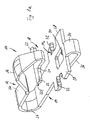
- FIG. 1a shows a contact 10 with a contact part 12 and a guide part 14.
- the contact part 12 has a spoon-like design Contact section 16. At one end of the contact section 16 closes a hook-shaped End section 18, the free end below the Contact section 16 lies and with projecting on the edge Wings 22 is formed.
- the other end of the contact section 16 closes first an intermediate section 24 and then one Bend 26 (about 180 °), so that the bend 26 subsequent guide part 14 at a distance below of the contact part 12 runs.
- the guide part 14 is widened at a distance from the bend 26 (by edge areas 28) and points in this section a central rectangular opening 30.
- Two tabs 32 are formed in the edge regions 28 and bent over the top 14o of the guide member 14. To do this, two cuts were made perpendicular and parallel to the outer edges of the edge regions 28
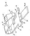
- the opening 30 replaced by a lowering 31 of the guide part 14, which continues into the free end region 34.
- the Tabs 32 run on both sides of the depression 31.
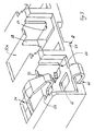
- FIG. 2 shows the arrangement of the contact 10 according to FIG 1a in a contact carrier 50, which has a receiving space 52 for the contact 10 and in the upper section has an opening 54 through which the contact part 12, in particular with its contact section 16, upwards can protrude.
- the end section 18 is designed and arranged in such a way that that its free end 20 with the wings 22 from below with slight preload against lateral boundaries 56 of the opening 54 abuts. At the same time, the wings bump 22 with their end faces 22f against corresponding inclined surfaces 58 below the lateral boundaries 56 extend from one Summary of Figures 2 and 3 results.
- the guide part 14 of the contact 10 is in lateral Guide slots 60 of the receiving space 52 assembled.
- the guide slots have a height that is slight is smaller than the height of the guide part 14 along the Edge areas 28, including the protruding tabs 32, so that the guide part 14 lies without play.
- the contact carrier 50 is located below the opening 30 a corresponding opening 62 is formed. In the recording room 52a according to FIG. 3, shown without contact this opening 62 is missing. If a contact according to FIG 1b can use the opening 62 through a recess in the Bottom of the contact carrier to be replaced, in which the Lowering 31 protrudes.
- the contact carrier 50 In the bottom area 64 of the contact carrier 50 there is a groove 66 designed to accommodate the free end 34 or the end part 36 of the contact 10, in such a way that the end part 36 has a lower one End face 68 of the contact carrier 50 protrudes, as in the figure 2 shows.
- the arrangement can be such that the End part 36 runs parallel to the lower end face 68 and therefore exactly horizontal.
- the contact section 16 When the contact section 16 is lowered further, it dips the end section 18 into the opening 30 of the guide part 14 or in the opening 62 of the contact carrier 50 a, (in the embodiment according to FIGS. 2, 3) so that this space is used to the height of the To limit the contact carrier 50 in total to a minimum.
- the inclined surfaces 58 support one safe, torque-free guidance of the end section 18 to in the area of the opening (s) 30, 62.
Landscapes
- Engineering & Computer Science (AREA)
- Artificial Intelligence (AREA)
- Computer Vision & Pattern Recognition (AREA)
- Physics & Mathematics (AREA)
- General Physics & Mathematics (AREA)
- Theoretical Computer Science (AREA)
- Coupling Device And Connection With Printed Circuit (AREA)
- Inspection Of Paper Currency And Valuable Securities (AREA)
- Radar Systems Or Details Thereof (AREA)
- Measurement Of The Respiration, Hearing Ability, Form, And Blood Characteristics Of Living Organisms (AREA)
- Contacts (AREA)
- Details Of Connecting Devices For Male And Female Coupling (AREA)
- Push-Button Switches (AREA)
Abstract
Description
- der Kontakt besitzt einen, in einem unteren Abschnitt des Kontaktträgers ortsfest montierbaren Führungsteil und
- einen, in einem oberen Abschnitt des Kontaktträgers beweglich montierbaren Kontaktteil,
- der Kontaktteil weist einen, im unbelasteten Zustand durch eine Öffnung im oberen Abschnitt des Kontaktträgers vorstehenden, nach außen gewölbten Kontaktabschnitt auf, an den sich auf einer Seite über einen Zwischenabschnitt der Führungsteil anschließt und an den sich auf einer gegenüberliegenden Seite ein hakenförmig gestalteter Endabschnitt anschließt, dessen freies Ende unterhalb des gewölbten Kontaktabschnittes liegt und mit randseitig vorstehenden Flügeln zur Führung im Kontaktteil ausgebildet ist.
- einen Raum zur Aufnahme mindestens eines Kontaktes der vorgenannten Art,
- eine Aussparung im oberen Abschnitt, durch die der Kontakt mit einem Kontaktabschnitt seines Kontaktteils im unbelasteten Zustand hindurchragt,
- im Bereich der Flügel des Kontaktteils angeordnete, einen Aufnahmeraum für den Kontakt begrenzende Schrägflächen, entlang der die Flügel des Kontaktes im belasteten Zustand des Kontaktabschnitts spannungsfrei in Richtung auf den Führungsteil des Kontaktes gleiten.
- Figur 1a:
- eine perspektivische Ansicht einer ersten Ausführungsform eines Kontaktes
- Figur 1b:
- eine perspektivische Ansicht einer zweiten Ausführungsform eines Kontaktes
- Figur 2:
- einen Längsschnitt durch einen Kontaktträger mit eingelegtem Kontakt
- Figur 3:
- eine perspektivische Ansicht eines Kontaktträgers mit einem eingelegten Kontakt.
Claims (14)
- Kontakt (10) zur Aufnahme in einem Kontaktträger (50), mit folgenden Merkmalen:1.1 der Kontakt (10) besitzt einen, in einem unteren Abschnitt des Kontaktträgers (50) ortsfest montierbaren Führungsteil (14), und1.2 einen, in einem oberen Abschnitt des Kontaktträgers (50) beweglich montierbaren Kontaktteil (12),1.3 der Kontaktteil (12) weist einen, im unbelasteten Zustand durch eine Öffnung (54) im oberen Abschnitt des Kontaktträgers (50) vorstehenden, nach außen gewölbten Kontaktabschnitt (16) auf, an den sich auf einer Seite über einen Zwischenabschnitt (24) der Führungsteil (14) anschließt und an den sich auf einer gegenüberliegenden Seite ein hakenförmig gestalteter Endabschnitt (18) anschließt, dessen freies Ende (20) unterhalb des gewölbten Kontaktabschnittes (16) liegt und mit randseitig vorstehenden Flügeln (22) zur Führung im Kontaktträger (50) ausgebildet ist.
- Kontakt nach Anspruch 1, dessen Führungsteil (14), in Verlängerung des Zwischenabschnitts (24) und einer daran anschließenden Umbiegung (26) im Abstand unterhalb des Kontaktteils (12) verläuft und unterhalb des Kontaktabschnitts (16) eine Öffnung (30) aufweist, die so groß ist, daß der hakenförmig gestaltete Endabschnitt (18) des Kontaktteils (12) im belasteten Zustand in die Öffnung (30) eintauchen kann.
- Kontakt nach Anspruch 1, dessen Führungsteil (14), in Verlängerung des Zwischenabschnitts (24) und einer daran anschließenden Umbiegung (26) im Abstand unterhalb des Kontaktteils (12) verläuft und unterhalb des Kontaktabschnitts (16) eine vom Kontaktabschnitt (16) wegweisende Absenkung (31) aufweist, die in ein freies Ende (34) des Führungsteils (14) übergeht.
- Kontakt nach Anspruch 3, bei dem die Absenkung (31) zwischen beidseitig der Absenkung (31) verlaufenden randseitigen Abschnitten (28) des Führungsteils (14) verläuft.
- Kontakt nach Anspruch 1, dessen Führungsteil (14) entlang seiner randseitigen Abschnitte (28) auf den Kontaktteil (12) vorstehende Laschen (32) aufweist.
- Kontakt nach Anspruch 1, dessen Führungsteil (14) an seinem freien Ende (34) nach unten umgebogen ist.
- Kontakt nach Anspruch 1, dessen Kontaktabschnitt (16) löffelartig gewölbt ist.
- Kontaktträger (50) mit einem Aufnahmeraum (52) zur Aufnahme mindestens eines Kontaktes (10) nach einem der Ansprüche 1 bis 7, mit einer Öffnung (54) im oberen Abschnitt, durch die der Kontakt (10) mit seinem Kontaktabschnitt (16) im unbelasteten Zustand hindurchragt und im Bereich der Flügel (22) des Kontaktteils (12) angeordneten, den Aufnahmeraum (52) für den Kontakt (10) begrenzenden Schrägflächen (58), entlang der die Flügel (22) des Kontaktes (10) im belasteten Zustand des Kontaktabschnitts (12) spannungsfrei in Richtung auf den Führungsteil (14) des Kontaktes (10) gleiten.
- Kontaktträger nach Anspruch 8, bei dem die Schrägflächen (58) benachbart zu seitlichen Endabschnitten der Flügel (22) verlaufen.
- Kontaktträger nach Anspruch 8 mit einer Öffnung (62) in Verlängerung der Öffnung (30) des Führungsabschnitts (14) des Kontaktes (10).
- Kontaktträger nach Anspruch 8 mit zwei im wesentlichen parallel zum Führungsteil (14) verlaufenden, randseitig den Aufnahmeraum (52) begrenzenden Führungsschlitzen (60), deren Höhe maximal der Dicke des Führungsteils (14) in seinen randseitigen Abschnitten (28) entspricht.
- Kontaktträger nach Anspruch 8 mit einer nutförmigen Vertiefung (66) entlang seiner unteren Stirnfläche (68) zur Aufnahme eines freien Endes (36) des Führungsteils (14) des Kontaktes (10) derart, daß das freie Ende (36) des Führungsteils (14) mit seiner Unterseite die untere Stirnfläche (68) des Kontaktträgers (50) überragt.
- Kontaktträger nach Anspruch 8 der unterhalb einer Absenkung (31) des Führungsteils (14) des Kontakts (10) eine korrespondierende Ausnehmung aufweist.
- Kontaktträger nach Anspruch 8, bei dem die Kontaktflügel (22) gegen korrespondierende Begrenzungen (56) des Kontaktträgers unterseitig anliegen.
Applications Claiming Priority (2)
| Application Number | Priority Date | Filing Date | Title |
|---|---|---|---|
| DE10027600 | 2000-06-02 | ||
| DE10027600A DE10027600C1 (de) | 2000-06-02 | 2000-06-02 | Kontakt zur Aufnahme in einem Kontaktträger sowie zugehöriger Kontaktträger |
Publications (2)
| Publication Number | Publication Date |
|---|---|
| EP1160926A1 true EP1160926A1 (de) | 2001-12-05 |
| EP1160926B1 EP1160926B1 (de) | 2004-05-19 |
Family
ID=7644617
Family Applications (1)
| Application Number | Title | Priority Date | Filing Date |
|---|---|---|---|
| EP01107661A Expired - Lifetime EP1160926B1 (de) | 2000-06-02 | 2001-03-28 | Kontakt zur Aufnahme in einem Kontaktträger sowie zugehöriger Kontaktträger |
Country Status (4)
| Country | Link |
|---|---|
| EP (1) | EP1160926B1 (de) |
| AT (1) | ATE267475T1 (de) |
| DE (2) | DE10027600C1 (de) |
| HK (1) | HK1042595B (de) |
Cited By (1)
| Publication number | Priority date | Publication date | Assignee | Title |
|---|---|---|---|---|
| FR2968466A1 (fr) * | 2010-12-07 | 2012-06-08 | Injection Haute Prec | Contact et connecteur de carte a microcircuit |
Families Citing this family (9)
| Publication number | Priority date | Publication date | Assignee | Title |
|---|---|---|---|---|
| JP3595939B2 (ja) * | 2002-03-29 | 2004-12-02 | 日本航空電子工業株式会社 | コネクタ |
| DE10318524B4 (de) * | 2002-05-08 | 2006-06-08 | Tyco Electronics Nederland B.V. | Elektrischer Verbinder mit einer Anschlagfläche für eine Kontaktfeder |
| DE10238661B3 (de) * | 2002-08-23 | 2004-02-26 | Lumberg Connect Gmbh & Co. Kg | Elektrische Kontaktiervorrichtung, insbesondere zur Verbindung einer Spannungsquelle mit einer elektronischen Schaltung |
| WO2005036701A1 (en) * | 2003-09-30 | 2005-04-21 | Molex Incorporated | Electrical connector |
| JP4170278B2 (ja) | 2004-03-19 | 2008-10-22 | タイコエレクトロニクスアンプ株式会社 | コンタクト及び電気コネクタ |
| CN2711921Y (zh) * | 2004-05-20 | 2005-07-20 | 上海莫仕连接器有限公司 | 用户身份识别模块卡连接器 |
| DE102004059776A1 (de) | 2004-09-17 | 2006-04-06 | Deutsches Zentrum für Luft- und Raumfahrt e.V. | Brennstoffzellensystem |
| DE102016108319B4 (de) * | 2016-05-04 | 2018-08-02 | Amphenol-Tuchel Electronics Gmbh | Schaltfederanordnung |
| DE202017006700U1 (de) | 2017-03-09 | 2018-01-25 | HARTING Electronics GmbH | Kontaktträger |
Citations (5)
| Publication number | Priority date | Publication date | Assignee | Title |
|---|---|---|---|---|
| EP0810689A2 (de) * | 1996-05-08 | 1997-12-03 | THOMAS & BETTS CORPORATION | Batterieverbinder |
| US5746626A (en) * | 1996-10-11 | 1998-05-05 | Bourns, Inc. | Electrical connector assembly |
| EP0866528A1 (de) * | 1997-03-21 | 1998-09-23 | Molex Incorporated | Elektrischer Verbinder mit Werkzeugeingriffarm |
| DE29911558U1 (de) * | 1999-07-02 | 1999-09-09 | Dieter Hölzle Technik-Projekte GmbH, 75392 Deckenpfronn | Kontaktelement mit einem Gehäuse, in dem mindestens eine Kontaktfeder gehalten ist |
| DE19829551A1 (de) * | 1998-07-02 | 2000-01-20 | Amphenol Tuchel Elect | Kontaktträger |
Family Cites Families (4)
| Publication number | Priority date | Publication date | Assignee | Title |
|---|---|---|---|---|
| DE4118312C2 (de) * | 1991-06-04 | 1995-03-09 | Amphenol Tuchel Elect | Kontaktsatz für eine Kontaktzonen aufweisende Karte |
| FR2714539B1 (fr) * | 1993-12-24 | 1996-01-26 | Itt Composants Instr | Connecteur électrique pour le raccordement d'une carte à mémoire électronique. |
| DE4411345C1 (de) * | 1994-03-31 | 1995-05-24 | Amphenol Tuchel Elect | Kontaktschalter |
| WO1997045900A1 (en) * | 1996-05-31 | 1997-12-04 | The Whitaker Corporation | Rechargeable battery connector |
-
2000
- 2000-06-02 DE DE10027600A patent/DE10027600C1/de not_active Expired - Fee Related
-
2001
- 2001-03-28 EP EP01107661A patent/EP1160926B1/de not_active Expired - Lifetime
- 2001-03-28 AT AT01107661T patent/ATE267475T1/de not_active IP Right Cessation
- 2001-03-28 DE DE50102309T patent/DE50102309D1/de not_active Expired - Lifetime
-
2002
- 2002-05-31 HK HK02104182.8A patent/HK1042595B/zh not_active IP Right Cessation
Patent Citations (5)
| Publication number | Priority date | Publication date | Assignee | Title |
|---|---|---|---|---|
| EP0810689A2 (de) * | 1996-05-08 | 1997-12-03 | THOMAS & BETTS CORPORATION | Batterieverbinder |
| US5746626A (en) * | 1996-10-11 | 1998-05-05 | Bourns, Inc. | Electrical connector assembly |
| EP0866528A1 (de) * | 1997-03-21 | 1998-09-23 | Molex Incorporated | Elektrischer Verbinder mit Werkzeugeingriffarm |
| DE19829551A1 (de) * | 1998-07-02 | 2000-01-20 | Amphenol Tuchel Elect | Kontaktträger |
| DE29911558U1 (de) * | 1999-07-02 | 1999-09-09 | Dieter Hölzle Technik-Projekte GmbH, 75392 Deckenpfronn | Kontaktelement mit einem Gehäuse, in dem mindestens eine Kontaktfeder gehalten ist |
Cited By (1)
| Publication number | Priority date | Publication date | Assignee | Title |
|---|---|---|---|---|
| FR2968466A1 (fr) * | 2010-12-07 | 2012-06-08 | Injection Haute Prec | Contact et connecteur de carte a microcircuit |
Also Published As
| Publication number | Publication date |
|---|---|
| EP1160926B1 (de) | 2004-05-19 |
| ATE267475T1 (de) | 2004-06-15 |
| HK1042595B (zh) | 2005-01-14 |
| DE50102309D1 (de) | 2004-06-24 |
| HK1042595A1 (en) | 2002-08-16 |
| DE10027600C1 (de) | 2001-11-22 |
Similar Documents
| Publication | Publication Date | Title |
|---|---|---|
| DE3872312T2 (de) | Pruefsockel mit verbesserter kontakteinrastung. | |
| DE69837700T2 (de) | Sehr dünner elektrischer Verbinder für Chipkartenverbindung | |
| DE68917080T2 (de) | Elektrischer Verbinder für elektronische Gedächtniskarten, Verfahren der Verwirklichung eines derartigen Verbinders und Lese-Schreibvorrichtung mit diesem Verbinder. | |
| DE69509599T2 (de) | Buchse mit metallischem Halteteil | |
| DE69307741T2 (de) | Steckverbinder für die Kante einer gedruckten Schaltung | |
| DE69322046T2 (de) | Elektrischer Verbinder für die Kante einer Karte | |
| DE4417088C2 (de) | Kontaktiersystem für Chipkarten | |
| DE69417988T2 (de) | Leiterplattenrandverbinder mit Kontakten von verminderten Teilung | |
| DE10213600B4 (de) | Leitfähiges Glied | |
| EP0357816A1 (de) | Doppelflachfederkontakt | |
| CH647896A5 (de) | Elektrisches endkontaktglied und verbindungsvorrichtung. | |
| DE2161637A1 (de) | Elektrisches Verbindungselement, insbesondere zur Anbringung an Leiterplatten | |
| DE2054201B2 (de) | Zur Verwendung in einem elektrischen Steckverbinder bestimmtes elektrisches Kontaktelement | |
| EP0627104A1 (de) | Kontaktiereinrichtung für eine chipkarte | |
| DE1094329B (de) | Steckverbindung aus gleichartigen Steckverbindungsteilen | |
| EP0721236A2 (de) | Verriegelungsvorrichtung für einen Steckverbinder | |
| DE10324294A1 (de) | Elektrische Steckvorrichtung für eine Chipkarte mit einem verbesserten Schaltsystem | |
| EP1160926B1 (de) | Kontakt zur Aufnahme in einem Kontaktträger sowie zugehöriger Kontaktträger | |
| DE3931508A1 (de) | Chipkartenleser | |
| DE10061533A1 (de) | Selbsttragende Kontaktfeder, insbesondere für einen Smartcard-Connector | |
| EP1982387B1 (de) | Superflacher simblock | |
| EP0901186B1 (de) | Anschlusselement für Schirmkabel | |
| DE2106178B2 (de) | Elektrischer Kontakt | |
| CH628185A5 (en) | Connecting part for penetrating the insulation of an insulated conductor, and an electrical connector having such a connecting part | |
| EP0921594B1 (de) | Steckverbindungseinrichtung |
Legal Events
| Date | Code | Title | Description |
|---|---|---|---|
| PUAI | Public reference made under article 153(3) epc to a published international application that has entered the european phase |
Free format text: ORIGINAL CODE: 0009012 |
|
| AK | Designated contracting states |
Kind code of ref document: A1 Designated state(s): AT BE CH CY DE DK ES FI FR GB GR IE IT LI LU MC NL PT SE TR |
|
| AX | Request for extension of the european patent |
Free format text: AL;LT;LV;MK;RO;SI |
|
| 17P | Request for examination filed |
Effective date: 20020110 |
|
| AKX | Designation fees paid |
Free format text: AT BE CH CY DE DK ES FI FR GB GR IE IT LI LU MC NL PT SE TR |
|
| GRAP | Despatch of communication of intention to grant a patent |
Free format text: ORIGINAL CODE: EPIDOSNIGR1 |
|
| RTI1 | Title (correction) |
Free format text: CONTACT FOR RECEIVING IN A CONTACT CARRIER AND CORRESPONDING CONTACT CARRIER |
|
| GRAS | Grant fee paid |
Free format text: ORIGINAL CODE: EPIDOSNIGR3 |
|
| GRAA | (expected) grant |
Free format text: ORIGINAL CODE: 0009210 |
|
| AK | Designated contracting states |
Kind code of ref document: B1 Designated state(s): AT BE CH CY DE DK ES FI FR GB GR IE IT LI LU MC NL PT SE TR |
|
| PG25 | Lapsed in a contracting state [announced via postgrant information from national office to epo] |
Ref country code: IT Free format text: LAPSE BECAUSE OF FAILURE TO SUBMIT A TRANSLATION OF THE DESCRIPTION OR TO PAY THE FEE WITHIN THE PRESCRIBED TIME-LIMIT;WARNING: LAPSES OF ITALIAN PATENTS WITH EFFECTIVE DATE BEFORE 2007 MAY HAVE OCCURRED AT ANY TIME BEFORE 2007. THE CORRECT EFFECTIVE DATE MAY BE DIFFERENT FROM THE ONE RECORDED. Effective date: 20040519 Ref country code: FI Free format text: LAPSE BECAUSE OF FAILURE TO SUBMIT A TRANSLATION OF THE DESCRIPTION OR TO PAY THE FEE WITHIN THE PRESCRIBED TIME-LIMIT Effective date: 20040519 Ref country code: IE Free format text: LAPSE BECAUSE OF FAILURE TO SUBMIT A TRANSLATION OF THE DESCRIPTION OR TO PAY THE FEE WITHIN THE PRESCRIBED TIME-LIMIT Effective date: 20040519 Ref country code: TR Free format text: LAPSE BECAUSE OF FAILURE TO SUBMIT A TRANSLATION OF THE DESCRIPTION OR TO PAY THE FEE WITHIN THE PRESCRIBED TIME-LIMIT Effective date: 20040519 Ref country code: NL Free format text: LAPSE BECAUSE OF FAILURE TO SUBMIT A TRANSLATION OF THE DESCRIPTION OR TO PAY THE FEE WITHIN THE PRESCRIBED TIME-LIMIT Effective date: 20040519 |
|
| REG | Reference to a national code |
Ref country code: GB Ref legal event code: FG4D Free format text: NOT ENGLISH |
|
| REG | Reference to a national code |
Ref country code: CH Ref legal event code: EP |
|
| REG | Reference to a national code |
Ref country code: IE Ref legal event code: FG4D Free format text: GERMAN |
|
| REF | Corresponds to: |
Ref document number: 50102309 Country of ref document: DE Date of ref document: 20040624 Kind code of ref document: P |
|
| GBT | Gb: translation of ep patent filed (gb section 77(6)(a)/1977) |
Effective date: 20040712 |
|
| PG25 | Lapsed in a contracting state [announced via postgrant information from national office to epo] |
Ref country code: SE Free format text: LAPSE BECAUSE OF FAILURE TO SUBMIT A TRANSLATION OF THE DESCRIPTION OR TO PAY THE FEE WITHIN THE PRESCRIBED TIME-LIMIT Effective date: 20040819 Ref country code: GR Free format text: LAPSE BECAUSE OF FAILURE TO SUBMIT A TRANSLATION OF THE DESCRIPTION OR TO PAY THE FEE WITHIN THE PRESCRIBED TIME-LIMIT Effective date: 20040819 Ref country code: DK Free format text: LAPSE BECAUSE OF FAILURE TO SUBMIT A TRANSLATION OF THE DESCRIPTION OR TO PAY THE FEE WITHIN THE PRESCRIBED TIME-LIMIT Effective date: 20040819 |
|
| PG25 | Lapsed in a contracting state [announced via postgrant information from national office to epo] |
Ref country code: ES Free format text: LAPSE BECAUSE OF FAILURE TO SUBMIT A TRANSLATION OF THE DESCRIPTION OR TO PAY THE FEE WITHIN THE PRESCRIBED TIME-LIMIT Effective date: 20040830 |
|
| NLV1 | Nl: lapsed or annulled due to failure to fulfill the requirements of art. 29p and 29m of the patents act | ||
| REG | Reference to a national code |
Ref country code: IE Ref legal event code: FD4D |
|
| REG | Reference to a national code |
Ref country code: HK Ref legal event code: GR Ref document number: 1042595 Country of ref document: HK |
|
| ET | Fr: translation filed | ||
| PLBE | No opposition filed within time limit |
Free format text: ORIGINAL CODE: 0009261 |
|
| STAA | Information on the status of an ep patent application or granted ep patent |
Free format text: STATUS: NO OPPOSITION FILED WITHIN TIME LIMIT |
|
| PG25 | Lapsed in a contracting state [announced via postgrant information from national office to epo] |
Ref country code: AT Free format text: LAPSE BECAUSE OF NON-PAYMENT OF DUE FEES Effective date: 20050328 Ref country code: LU Free format text: LAPSE BECAUSE OF NON-PAYMENT OF DUE FEES Effective date: 20050328 Ref country code: CY Free format text: LAPSE BECAUSE OF FAILURE TO SUBMIT A TRANSLATION OF THE DESCRIPTION OR TO PAY THE FEE WITHIN THE PRESCRIBED TIME-LIMIT Effective date: 20050328 |
|
| PG25 | Lapsed in a contracting state [announced via postgrant information from national office to epo] |
Ref country code: MC Free format text: LAPSE BECAUSE OF NON-PAYMENT OF DUE FEES Effective date: 20050331 Ref country code: BE Free format text: LAPSE BECAUSE OF NON-PAYMENT OF DUE FEES Effective date: 20050331 Ref country code: LI Free format text: LAPSE BECAUSE OF NON-PAYMENT OF DUE FEES Effective date: 20050331 Ref country code: CH Free format text: LAPSE BECAUSE OF NON-PAYMENT OF DUE FEES Effective date: 20050331 |
|
| 26N | No opposition filed |
Effective date: 20050222 |
|
| BERE | Be: lapsed |
Owner name: *AMPHENOL-TUCHEL ELECTRONICS G.M.B.H. Effective date: 20050331 |
|
| REG | Reference to a national code |
Ref country code: CH Ref legal event code: PL |
|
| BERE | Be: lapsed |
Owner name: *AMPHENOL-TUCHEL ELECTRONICS G.M.B.H. Effective date: 20050331 |
|
| PG25 | Lapsed in a contracting state [announced via postgrant information from national office to epo] |
Ref country code: PT Free format text: LAPSE BECAUSE OF NON-PAYMENT OF DUE FEES Effective date: 20041019 |
|
| REG | Reference to a national code |
Ref country code: FR Ref legal event code: PLFP Year of fee payment: 15 |
|
| PGFP | Annual fee paid to national office [announced via postgrant information from national office to epo] |
Ref country code: DE Payment date: 20150324 Year of fee payment: 15 |
|
| PGFP | Annual fee paid to national office [announced via postgrant information from national office to epo] |
Ref country code: FR Payment date: 20150319 Year of fee payment: 15 Ref country code: GB Payment date: 20150324 Year of fee payment: 15 |
|
| REG | Reference to a national code |
Ref country code: DE Ref legal event code: R119 Ref document number: 50102309 Country of ref document: DE |
|
| GBPC | Gb: european patent ceased through non-payment of renewal fee |
Effective date: 20160328 |
|
| REG | Reference to a national code |
Ref country code: FR Ref legal event code: ST Effective date: 20161130 |
|
| PG25 | Lapsed in a contracting state [announced via postgrant information from national office to epo] |
Ref country code: GB Free format text: LAPSE BECAUSE OF NON-PAYMENT OF DUE FEES Effective date: 20160328 Ref country code: FR Free format text: LAPSE BECAUSE OF NON-PAYMENT OF DUE FEES Effective date: 20160331 Ref country code: DE Free format text: LAPSE BECAUSE OF NON-PAYMENT OF DUE FEES Effective date: 20161001 |