EP1160921A2 - Connecteur pour connecter des fils à une carte à circuits - Google Patents
Connecteur pour connecter des fils à une carte à circuits Download PDFInfo
- Publication number
- EP1160921A2 EP1160921A2 EP01112515A EP01112515A EP1160921A2 EP 1160921 A2 EP1160921 A2 EP 1160921A2 EP 01112515 A EP01112515 A EP 01112515A EP 01112515 A EP01112515 A EP 01112515A EP 1160921 A2 EP1160921 A2 EP 1160921A2
- Authority
- EP
- European Patent Office
- Prior art keywords
- contact
- connector according
- housing
- electrical line
- circuit board
- Prior art date
- Legal status (The legal status is an assumption and is not a legal conclusion. Google has not performed a legal analysis and makes no representation as to the accuracy of the status listed.)
- Granted
Links
Images


Classifications
-
- H—ELECTRICITY
- H01—ELECTRIC ELEMENTS
- H01R—ELECTRICALLY-CONDUCTIVE CONNECTIONS; STRUCTURAL ASSOCIATIONS OF A PLURALITY OF MUTUALLY-INSULATED ELECTRICAL CONNECTING ELEMENTS; COUPLING DEVICES; CURRENT COLLECTORS
- H01R12/00—Structural associations of a plurality of mutually-insulated electrical connecting elements, specially adapted for printed circuits, e.g. printed circuit boards [PCB], flat or ribbon cables, or like generally planar structures, e.g. terminal strips, terminal blocks; Coupling devices specially adapted for printed circuits, flat or ribbon cables, or like generally planar structures; Terminals specially adapted for contact with, or insertion into, printed circuits, flat or ribbon cables, or like generally planar structures
- H01R12/70—Coupling devices
- H01R12/82—Coupling devices connected with low or zero insertion force
Definitions
- the invention relates to a connector, in particular zero-force connector, for connecting electrical cables to a printed circuit board.
- Connectors are for a variety of uses known. They are therefore in a wide variety of embodiments and usually in large quantities, for example in the area of so-called "brown goods", used and subject to their respective use the most diverse requirements. So are in the Usually in addition to simple and inexpensive production, low Height, large holding forces or fully automatic assembly also one Strain relief or reliable contacting. Furthermore are as zero insertion force or ZIF connectors known connectors are known, which must be designed such that none during a plugging or pulling process significant compressive or tensile forces occur.
- the design of the Connectors basically between two types of connection differentiate.
- the direct plug-in in which a connector is so on a Printed circuit board is inserted that the contact elements of the connector Contact directly with the printed conductor tracks of a printed circuit board be
- the indirect plug in which one as a two-part Plug connection trained connector is used, one of which Part mounted on the circuit board and the other part on the electrical Line is struck.
- the present invention primarily aims Plug connector for indirect plugging, but can be minor modifications without further ado also for direct insertion use that in general a special design of the circuit board required.
- circuit board or board are within the scope of the present Invention printed circuits with circuit patterns on one or both Sides and multilayer printed circuit boards, so-called multilayer, understood.
- circuit boards are usually with metallized holes Fastening components using solder connections or Provide press-fit connections.
- the components for example the one on the Circuit board part of a connector for indirect Plug, have for this purpose contact elements in their PCB-side connection area as contact legs, which in the Bores of the circuit board are inserted, are formed.
- soldering for example by soldering methods such as wave soldering
- the Contact legs soldered to the underside of the circuit board, whereas the Press the contact legs into elastically deformable or rigid press-in pins through which the mechanical stress is reduced at the same time solderless electrical connection is established.
- connectors for connecting electrical Lines known to a circuit board
- the one made of plastic or metal have existing housing that primarily mechanical Protection of the components of a connector and security against touching electrical parts.
- this can Housing also for other functions, such as one Locking, polarization, coding, electrical shielding, sealing or a strain relief.
- electrical lines both one or more cores with, are to be seen Insulating sleeves, a jacket to protect structural elements or Shields for shielding cables, especially flexible Cables, flat cables, hose lines, shielded cables or Coaxial lines, as well as cables that are suitable for fixed installation and a jacket made of plastic or rubber and optionally one have additional metal sheath.
- the disadvantage of the known connectors is the relative complex way with which a strain relief is realized.
- the complicated and unreliable contacting is also unsatisfactory of the electrical lines.
- the invention has for its object to provide a connector for connecting electrical lines to a circuit board, with which a reliable strain relief and reliable contacting of the electrical line can be achieved in a comparatively simple manner.
- a connector of the aforementioned type consisting of a fastenable on the circuit board housing, which is provided on a front side with spaced windows and serves as a contact carrier for receiving contact elements in these areas, and in one of the windows Opposite opening of the insertable plug-in element, which can be locked in a first securing position and a second end position in the housing and has a support surface that positions the electrical line and has a recess, the electrical line between the support surface and one that can be locked in place on the insert element Clamping element, on which at least one projection engaging in the recess is arranged, can be clamped, and the insulation-free end of a wire of the electrical line has a plug-in area of a single contact located in the housing elements contacted in the end position of the insert element inserted into the housing and a connection area of the contact element which can be led out of the windows can be connected in an electrically conductive manner to a conductor track of the circuit board.
- Such a connector is based on the knowledge that a reliable strain relief can be achieved if one of the Clamping element arranged projection in the recess of the Insert element engages. Because in this way the between the Insert element and the clamping element clamped electrical conductors also pressed into the recess and thereby additionally positively fixed.
- For reliable contacting of the electrical Line also contributes to the fact that the insertion element is initially in a Secured position in the housing can be locked before it by another Insert in the end position in the housing, in which the Contact elements are contacted. Because the contacting is only at already inserted insert element and housing takes place in addition to targeted and constant contacting of the Contact elements also an effective protection against accidental contact if necessary, already live with the contact electrical line ensured.
- Insert element and the clamping element as separate components or to connect with each other via a film hinge.
- the insert element on both sides of the support surface To provide guide surfaces for the electrical line.
- the electrical cable can be positioned on the support surface thereby guarantee.
- the insert element has at least one cam which is form-fitting engages in a recess of the electrical line. This allows especially the location of the free end of the electrical line on the Define the insert element exactly, so that the impression of the electrical Lead into the recess through the projection without affecting the Positioning of the electrical line on the contact surface remains.
- the river Oder the cams can either be on the guide surfaces or on a be placed anywhere on the support surface. The latter is in Generally, however, only if the loss of one or to implement multiple wires.
- the insertion element is in the direction of insertion provided first and second locking lugs arranged one behind the other on a correspondingly designed fastening section of the housing for locking the insert element in the securing position and End position can be determined.
- first and second locking lugs arranged one behind the other on a correspondingly designed fastening section of the housing for locking the insert element in the securing position and End position can be determined.
- Connector is the clamping element at its front in the direction of insertion End face with an oblique ramp surface that is spaced from the Support surface in the end position of the insert element, the plug-in area of a contact element on the associated insulation-free wires electrical line.
- the contact surface with the free end of the electrical line receiving slot may be provided, in which End position of the insert element of the plug area of a contact element the associated insulation-free wire of the electrical line in the area of Slot contacted.
- the slot is on simple way an exact location of the contact surface between the insulation-free wires of the electrical line and the contact elements defined and thus favors a reliable contact.
- Training of the connector is also proposed on the Clamping element facing away from the insert element Provide a stop for the electrical line through the slot. Such further training allows a contact game between adjust the contact elements and the electrical cable. By doing namely the length of the section of the electrical cable is dimensioned so that the insulation-free wires the electrical line through the free end of the electrical line in the area of the slot slightly from the Lift off the contact surface, the distance to the contact elements can vary become.
- Conduct the projection a rectangular, triangular or cross section has a rounded shape.
- the recess of the insert element can adapted to the respective application also different be formed, for example as a continuous opening or trough-shaped recess.
- the contact elements are expedient formed in their plug-in area as a resilient fork contact, the one in essential hook-shaped contact holder for locking in the housing having. This enables secure attachment with simple assembly the contact elements in the housing, even if the Connection area of the contact elements through the contact surface on the electrical line is depressed.
- the Contact elements in their plug area have a leg that with is provided with a curvature which corresponds to a in the end position trained recess snaps into place.
- Such Design offers the advantage that an additional one Locking of the insert element in the housing and on the other reaching the end position in both acoustic and haptic Terms is displayed.
- the curvature can be both convex and be concave on the leg. In the latter case, the Recess a correspondingly shaped projection on the Insert element to be provided.
- the contact elements in their connection area with straight or angled contact legs provided, which are pressed into the circuit board or soldered to it with such a standing or lying connector ensure a permanent electrical connection to the circuit board.
- the housing it is proposed to design the housing as an insulating body, so that additional means to isolate the individual contact elements, become dispensable.
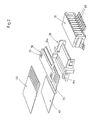
- the connector shown in Fig. 1 has an insulating body formed housing 10, which is attachable to a circuit board 50.
- the housing 10 is spaced apart from one another on one end face Windows 11 and on the opposite side with an opening 12 provided.
- the interior of the housing 10 is in the area of the windows 11 designed as a contact carrier for receiving contact elements 60, whose connection area is led out of the windows 11 in order to Conductor tracks 51 of the circuit board 50 to be electrically connected.
- the contact elements 60 are designed as resilient fork contacts and have as a contact holder 61 hook-shaped on its upper leg 62 Projections on the on the window 11 facing portion of the upper inner surface 15 of the housing 10 are locked, as in Fig. 3a and 4a can be seen.
- Insert element 20 In the opening 12 is an insertion element 20, which has a flat contact surface 21 for a flat cable 40, insertable. Insert element 20 is with a recess extending transversely across the bearing surface 21 22 provided. Guide surfaces are located on both sides of the support surface 21 23 for the flat cable 40 and cams 24, which are on the support surface 21 positioned flat line 40 in recesses 42 present thereon intervene positively. Are on the outside of the guide surfaces 23 two arranged one behind the other in the direction of insertion of the insert element 20 Lugs 25, 26 formed. When inserting insert element 20 in the housing 10, the locking lugs 25, 26 act on both sides of the opening 12 arranged fastening sections 13 together. Through the Latches 25, the insertion element 20 in a first Secured position I locked in the housing 10.
- the guide surfaces 23 come orthogonally extending stop surfaces 29 on the outside of the Insert element 20 are arranged to lie on the housing 10, so that a continuous insertion of the insertion element 20 is excluded.
- the fastening sections 13 are perpendicular to Plug direction of the insert element 20 is resilient, which means the insert element 20 almost without resistance in the Safety position I and end position II can be introduced.
- the connector therefore represents a zero force or ZIF connector.
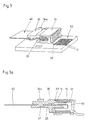
- Clamping element 30 is arranged pivotably.
- the clamping element 30 is on its side opposite the film hinge 32 with a Provided locking hook 34, which in the case of the insertion element 20 pivoted clamping element 30 on the film hinge 32nd opposite side of the insert element 20 can be locked in place, around the flat line 40 positioned on the support surface 21 between the Fix insert element 20 and the clamping element 30 by clamping.
- On the clamping element 30 is formed a projection 31, which at about Insert element 20 pivoted clamping element 30 into the recess 22 engages.
- the flat line 40 positioned on the support surface 21 becomes hereby also pressed into the recess 22 and into a fold 43 deformed. In this way, high holding forces and a reliable strain relief.
- the clamping element 30 is on its front end in the direction of insertion also provided with an inclined ramp 33 which is parallel to the Projection 31 extends and extends over insert element 20 pivoted clamping element 30 spaced from that on the support surface 21 positioned flat line 40 extends.
- the run-up surface 33 runs when the insertion element 20 is inserted into the Housing 10 shortly before reaching the end position II to one above the Opening 12 of the housing 10 formed insertion slope 14, which the ramp surface 33 between the inner surface 15 and the inside of the Housing 10 located plugging area of the contact elements 60 forces.
- the upper leg 62 of the contact elements 60 in the end position II to an associated insulation-free contact area Core 41 of the electrical line 40 is depressed.
- the electrical contacting of the flat cable 40 Only takes place in the end position II the electrical contacting of the flat cable 40, whereas effective protection against accidental contact is reached as soon as Secure position I is guaranteed.
- the contact elements 60 instruct a curvature 64 on its lower leg 63.
- the bottom of the Insert element 20 corresponds to a curvature 64 trained recess 64a provided.
- the arrangement of the curvature 64 on the leg 63 or the recess 64a on the Insert element 20 is such that in the end position II of the Inserted housing 20 insert 20 a latching Contact elements 60 and insert element 20 takes place, which to a contributes to secure contacting. It is also this way perceptible both acoustically and haptically when the insert element 20 reaches the end position II.
- the connector shown in Fig. 1 is a surface mount Component (SMD) trained and therefore within the so-called "pick-and-place technology" processable.
- SMD surface mount Component
- 1a and 1b are alternative Embodiments shown in which the connection area of the Contact elements 60 has straight or angled contact legs, which in metallized holes in the circuit board 50 are pressed or plugged in and soldered.
- the windows 11 additionally extend on the underside of the housing 10 to a grid dimension corresponding to the respective application to be able to provide.
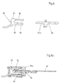
- the embodiment shown in Fig. 2 differs from that 1 only in that the insertion element 20th and the clamping element 30 does not have a film hinge with one another connected, but are formed as separate components.
- the clamping element 30 is provided with recesses 35 into which Insert element 20 correspondingly designed locking hooks 34a on the Insert element 20 arranged clamping element 30 engage, as well 3 and 3a also show such a connector give recognition.
- FIGS. 2a and 4 to 4b is missing another embodiment of a connector, the run-up surface 33.
- the contact surface 21 of the insert element 20 is provided with a the free end of the flat cable 40 receiving and thus an accurate Location of the contact surface between the flat line 40 and the Provide contact elements 60 defining slot 27, as special can be clearly seen in FIGS. 4a and 4b.
- Flat line 40 passed through is on the clamping element 30
- a stop 28 furthermore faces away from the underside of the insertion element 20 educated.
- 5 to 5c are finally different possibilities for Design of the projection 31 and the receiving recess 22 shown.
- several projections 31 can be provided, as can be seen in FIGS. 5b and 5c.
- the projection 31 can over it also be provided with different cross-sectional shapes, for example rectangular as in FIGS. 3a and 4a or triangular as in the aforementioned Characters.
- the recess 22 of the insert element 20 also be different and the respective Use case according to, for example, a continuous opening such as 3a, 4a and 5 or a trough-shaped recess as in the 5a to 5c.
- the connector described above is particularly suitable to be used as a zero force connector.
- the connector is also characterized by high holding forces and a reliable Strain relief.
- it is suitable for both conventional push-through technology as well as for the increasingly widespread SMT.
- Last but not least, it enables the same housing Processing different electrical lines 40 and thus offers also creating jumpers.
Applications Claiming Priority (2)
| Application Number | Priority Date | Filing Date | Title |
|---|---|---|---|
| DE20009788U | 2000-05-31 | ||
| DE20009788U DE20009788U1 (de) | 2000-05-31 | 2000-05-31 | Steckverbinder zum Anschließen elektrischer Leitungen an eine Leipterplatte |
Publications (3)
| Publication Number | Publication Date |
|---|---|
| EP1160921A2 true EP1160921A2 (fr) | 2001-12-05 |
| EP1160921A3 EP1160921A3 (fr) | 2003-01-08 |
| EP1160921B1 EP1160921B1 (fr) | 2004-03-31 |
Family
ID=7942282
Family Applications (1)
| Application Number | Title | Priority Date | Filing Date |
|---|---|---|---|
| EP01112515A Expired - Lifetime EP1160921B1 (fr) | 2000-05-31 | 2001-05-23 | Connecteur pour connecter des fils à une carte à circuits |
Country Status (2)
| Country | Link |
|---|---|
| EP (1) | EP1160921B1 (fr) |
| DE (2) | DE20009788U1 (fr) |
Cited By (1)
| Publication number | Priority date | Publication date | Assignee | Title |
|---|---|---|---|---|
| DE102020130750A1 (de) | 2020-11-20 | 2022-05-25 | Huber Automotive Ag | Leiterplatten-Anordnung, Verfahren zum Herstellen einer Leiterplatten-Anordnung und Steuereinheit |
Families Citing this family (3)
| Publication number | Priority date | Publication date | Assignee | Title |
|---|---|---|---|---|
| DE10125656A1 (de) * | 2001-05-25 | 2002-11-28 | Delphi Tech Inc | Zugentlastungsvorrichtung |
| DE10327043A1 (de) * | 2003-06-16 | 2005-01-05 | BSH Bosch und Siemens Hausgeräte GmbH | Zugentlastung für ein Elektrokabel |
| DE102015111675A1 (de) | 2015-07-17 | 2017-01-19 | Wago Verwaltungsgesellschaft Mbh | Steckverbinder und Verformungswerkzeug hierzu |
Citations (4)
| Publication number | Priority date | Publication date | Assignee | Title |
|---|---|---|---|---|
| US5474468A (en) * | 1992-09-14 | 1995-12-12 | Sumitomo Wiring Systems, Ltd. | Connector |
| US5759060A (en) * | 1996-01-16 | 1998-06-02 | Hon Hai Precision Ind. Co. Ltd. | Insulation displacement contact connector |
| JPH10308245A (ja) * | 1997-05-01 | 1998-11-17 | Yazaki Corp | フレキシブル導電体の固定方法及び固定構造 |
| US6062900A (en) * | 1998-11-30 | 2000-05-16 | Hon Hai Precision Ind. Co., Ltd. | ZIF FFC connector having a strain relief |
-
2000
- 2000-05-31 DE DE20009788U patent/DE20009788U1/de not_active Expired - Lifetime
-
2001
- 2001-05-23 EP EP01112515A patent/EP1160921B1/fr not_active Expired - Lifetime
- 2001-05-23 DE DE50101813T patent/DE50101813D1/de not_active Expired - Fee Related
Patent Citations (4)
| Publication number | Priority date | Publication date | Assignee | Title |
|---|---|---|---|---|
| US5474468A (en) * | 1992-09-14 | 1995-12-12 | Sumitomo Wiring Systems, Ltd. | Connector |
| US5759060A (en) * | 1996-01-16 | 1998-06-02 | Hon Hai Precision Ind. Co. Ltd. | Insulation displacement contact connector |
| JPH10308245A (ja) * | 1997-05-01 | 1998-11-17 | Yazaki Corp | フレキシブル導電体の固定方法及び固定構造 |
| US6062900A (en) * | 1998-11-30 | 2000-05-16 | Hon Hai Precision Ind. Co., Ltd. | ZIF FFC connector having a strain relief |
Non-Patent Citations (1)
| Title |
|---|
| PATENT ABSTRACTS OF JAPAN vol. 1999, no. 02, 26. Februar 1999 (1999-02-26) & JP 10 308245 A (YAZAKI CORP), 17. November 1998 (1998-11-17) & US 6 156 138 A (MOCHIDUKI) 5. Dezember 2000 (2000-12-05) * |
Cited By (1)
| Publication number | Priority date | Publication date | Assignee | Title |
|---|---|---|---|---|
| DE102020130750A1 (de) | 2020-11-20 | 2022-05-25 | Huber Automotive Ag | Leiterplatten-Anordnung, Verfahren zum Herstellen einer Leiterplatten-Anordnung und Steuereinheit |
Also Published As
| Publication number | Publication date |
|---|---|
| EP1160921A3 (fr) | 2003-01-08 |
| DE50101813D1 (de) | 2004-05-06 |
| DE20009788U1 (de) | 2000-09-07 |
| EP1160921B1 (fr) | 2004-03-31 |
Similar Documents
| Publication | Publication Date | Title |
|---|---|---|
| DE19736607C1 (de) | Leiterplattensteckbuchse | |
| DE3544838C2 (fr) | ||
| DE60036250T2 (de) | Modularer Jack-Verbinder mit Filtereinsatz und Kontakt dafür | |
| DE60003869T2 (de) | Elektrischer Verbinder | |
| DE202005002902U1 (de) | Elektrischer Steckverbinder | |
| DE102008060642B4 (de) | Steckverbinder mit Erdungsplatte | |
| DE2130855A1 (de) | Mehrfach-Steckverbindung | |
| DE4309039A1 (de) | Anschlußdose für abgeschirmte Kabel, insbesondere für Datenübertragungskabel | |
| DE2746273C2 (de) | Elektrischer Verbinder zum Befestigen eines Steckgehäuses auf einem Substrat | |
| EP0211357B1 (fr) | procédé d'installation d'un dispositif de contact sur une carte de circuits imprimés. | |
| EP0735616A2 (fr) | Connecteur électrique, notamment pour des plaquettes de circuits | |
| EP2091109B1 (fr) | Connecteur à fiches conductrices doté d'une connexion de masse | |
| DE60223319T2 (de) | Elektrischer Verbinder zum Aufnahme eines Steckers | |
| DE102006030712B4 (de) | Steckverbinder | |
| DE19726856C1 (de) | Flachstecker für elektrische Steckverbindungen | |
| DE3731413C2 (fr) | ||
| EP1160921B1 (fr) | Connecteur pour connecter des fils à une carte à circuits | |
| EP1111725B1 (fr) | Connecteur pour carte de circuit imprimé | |
| DE2517465C3 (de) | Steckverbinder | |
| DD297283A5 (de) | Kontaktgehaeuse mit kontaktelementen zum bestuecken von leiterplatten | |
| EP0402739A1 (fr) | Dispositif pour coupler électriquement des unités électriques enfichables | |
| DE202013104811U1 (de) | Elektrische Kontaktvorrichtung, insbesondere elektrische Printklemme und/oder Grundleiste | |
| DE102019111193B3 (de) | Schnittstelle mit Leiterplattenkontakt für Leiterplatte | |
| DE602004008094T2 (de) | Elektrischer verbinder für einen flexiblen flachleiter und schalteinrichtung | |
| WO2009065470A1 (fr) | Limiteur de tension enfichable et barre de terre |
Legal Events
| Date | Code | Title | Description |
|---|---|---|---|
| PUAI | Public reference made under article 153(3) epc to a published international application that has entered the european phase |
Free format text: ORIGINAL CODE: 0009012 |
|
| AK | Designated contracting states |
Kind code of ref document: A2 Designated state(s): AT BE CH CY DE DK ES FI FR GB GR IE IT LI LU MC NL PT SE TR |
|
| AX | Request for extension of the european patent |
Free format text: AL;LT;LV;MK;RO;SI |
|
| PUAL | Search report despatched |
Free format text: ORIGINAL CODE: 0009013 |
|
| AK | Designated contracting states |
Kind code of ref document: A3 Designated state(s): AT BE CH CY DE DK ES FI FR GB GR IE IT LI LU MC NL PT SE TR |
|
| AX | Request for extension of the european patent |
Free format text: AL;LT;LV;MK;RO;SI |
|
| 17P | Request for examination filed |
Effective date: 20030415 |
|
| 17Q | First examination report despatched |
Effective date: 20030606 |
|
| AKX | Designation fees paid |
Designated state(s): DE FR GB IT |
|
| GRAP | Despatch of communication of intention to grant a patent |
Free format text: ORIGINAL CODE: EPIDOSNIGR1 |
|
| GRAS | Grant fee paid |
Free format text: ORIGINAL CODE: EPIDOSNIGR3 |
|
| GRAA | (expected) grant |
Free format text: ORIGINAL CODE: 0009210 |
|
| AK | Designated contracting states |
Kind code of ref document: B1 Designated state(s): DE FR GB IT |
|
| REG | Reference to a national code |
Ref country code: GB Ref legal event code: FG4D Free format text: NOT ENGLISH |
|
| REG | Reference to a national code |
Ref country code: IE Ref legal event code: FG4D Free format text: GERMAN |
|
| REF | Corresponds to: |
Ref document number: 50101813 Country of ref document: DE Date of ref document: 20040506 Kind code of ref document: P |
|
| GBT | Gb: translation of ep patent filed (gb section 77(6)(a)/1977) |
Effective date: 20040510 |
|
| ET | Fr: translation filed | ||
| REG | Reference to a national code |
Ref country code: IE Ref legal event code: FD4D |
|
| PLBE | No opposition filed within time limit |
Free format text: ORIGINAL CODE: 0009261 |
|
| STAA | Information on the status of an ep patent application or granted ep patent |
Free format text: STATUS: NO OPPOSITION FILED WITHIN TIME LIMIT |
|
| 26N | No opposition filed |
Effective date: 20050104 |
|
| PGFP | Annual fee paid to national office [announced via postgrant information from national office to epo] |
Ref country code: DE Payment date: 20080602 Year of fee payment: 8 |
|
| PGFP | Annual fee paid to national office [announced via postgrant information from national office to epo] |
Ref country code: IT Payment date: 20080523 Year of fee payment: 8 |
|
| PGFP | Annual fee paid to national office [announced via postgrant information from national office to epo] |
Ref country code: GB Payment date: 20080522 Year of fee payment: 8 |
|
| GBPC | Gb: european patent ceased through non-payment of renewal fee |
Effective date: 20090523 |
|
| REG | Reference to a national code |
Ref country code: FR Ref legal event code: ST Effective date: 20100129 |
|
| PG25 | Lapsed in a contracting state [announced via postgrant information from national office to epo] |
Ref country code: FR Free format text: LAPSE BECAUSE OF NON-PAYMENT OF DUE FEES Effective date: 20090602 |
|
| PGFP | Annual fee paid to national office [announced via postgrant information from national office to epo] |
Ref country code: FR Payment date: 20080526 Year of fee payment: 8 |
|
| PG25 | Lapsed in a contracting state [announced via postgrant information from national office to epo] |
Ref country code: GB Free format text: LAPSE BECAUSE OF NON-PAYMENT OF DUE FEES Effective date: 20090523 |
|
| PG25 | Lapsed in a contracting state [announced via postgrant information from national office to epo] |
Ref country code: DE Free format text: LAPSE BECAUSE OF NON-PAYMENT OF DUE FEES Effective date: 20091201 |
|
| PG25 | Lapsed in a contracting state [announced via postgrant information from national office to epo] |
Ref country code: IT Free format text: LAPSE BECAUSE OF NON-PAYMENT OF DUE FEES Effective date: 20090523 |