EP1160921A2 - Connector for connecting wires to a circuit board - Google Patents
Connector for connecting wires to a circuit board Download PDFInfo
- Publication number
- EP1160921A2 EP1160921A2 EP01112515A EP01112515A EP1160921A2 EP 1160921 A2 EP1160921 A2 EP 1160921A2 EP 01112515 A EP01112515 A EP 01112515A EP 01112515 A EP01112515 A EP 01112515A EP 1160921 A2 EP1160921 A2 EP 1160921A2
- Authority
- EP
- European Patent Office
- Prior art keywords
- contact
- connector according
- housing
- electrical line
- circuit board
- Prior art date
- Legal status (The legal status is an assumption and is not a legal conclusion. Google has not performed a legal analysis and makes no representation as to the accuracy of the status listed.)
- Granted
Links
Images


Classifications
-
- H—ELECTRICITY
- H01—ELECTRIC ELEMENTS
- H01R—ELECTRICALLY-CONDUCTIVE CONNECTIONS; STRUCTURAL ASSOCIATIONS OF A PLURALITY OF MUTUALLY-INSULATED ELECTRICAL CONNECTING ELEMENTS; COUPLING DEVICES; CURRENT COLLECTORS
- H01R12/00—Structural associations of a plurality of mutually-insulated electrical connecting elements, specially adapted for printed circuits, e.g. printed circuit boards [PCB], flat or ribbon cables, or like generally planar structures, e.g. terminal strips, terminal blocks; Coupling devices specially adapted for printed circuits, flat or ribbon cables, or like generally planar structures; Terminals specially adapted for contact with, or insertion into, printed circuits, flat or ribbon cables, or like generally planar structures
- H01R12/70—Coupling devices
- H01R12/82—Coupling devices connected with low or zero insertion force
Definitions
- the invention relates to a connector, in particular zero-force connector, for connecting electrical cables to a printed circuit board.
- Connectors are for a variety of uses known. They are therefore in a wide variety of embodiments and usually in large quantities, for example in the area of so-called "brown goods", used and subject to their respective use the most diverse requirements. So are in the Usually in addition to simple and inexpensive production, low Height, large holding forces or fully automatic assembly also one Strain relief or reliable contacting. Furthermore are as zero insertion force or ZIF connectors known connectors are known, which must be designed such that none during a plugging or pulling process significant compressive or tensile forces occur.
- the design of the Connectors basically between two types of connection differentiate.
- the direct plug-in in which a connector is so on a Printed circuit board is inserted that the contact elements of the connector Contact directly with the printed conductor tracks of a printed circuit board be
- the indirect plug in which one as a two-part Plug connection trained connector is used, one of which Part mounted on the circuit board and the other part on the electrical Line is struck.
- the present invention primarily aims Plug connector for indirect plugging, but can be minor modifications without further ado also for direct insertion use that in general a special design of the circuit board required.
- circuit board or board are within the scope of the present Invention printed circuits with circuit patterns on one or both Sides and multilayer printed circuit boards, so-called multilayer, understood.
- circuit boards are usually with metallized holes Fastening components using solder connections or Provide press-fit connections.
- the components for example the one on the Circuit board part of a connector for indirect Plug, have for this purpose contact elements in their PCB-side connection area as contact legs, which in the Bores of the circuit board are inserted, are formed.
- soldering for example by soldering methods such as wave soldering
- the Contact legs soldered to the underside of the circuit board, whereas the Press the contact legs into elastically deformable or rigid press-in pins through which the mechanical stress is reduced at the same time solderless electrical connection is established.
- connectors for connecting electrical Lines known to a circuit board
- the one made of plastic or metal have existing housing that primarily mechanical Protection of the components of a connector and security against touching electrical parts.
- this can Housing also for other functions, such as one Locking, polarization, coding, electrical shielding, sealing or a strain relief.
- electrical lines both one or more cores with, are to be seen Insulating sleeves, a jacket to protect structural elements or Shields for shielding cables, especially flexible Cables, flat cables, hose lines, shielded cables or Coaxial lines, as well as cables that are suitable for fixed installation and a jacket made of plastic or rubber and optionally one have additional metal sheath.
- the disadvantage of the known connectors is the relative complex way with which a strain relief is realized.
- the complicated and unreliable contacting is also unsatisfactory of the electrical lines.
- the invention has for its object to provide a connector for connecting electrical lines to a circuit board, with which a reliable strain relief and reliable contacting of the electrical line can be achieved in a comparatively simple manner.
- a connector of the aforementioned type consisting of a fastenable on the circuit board housing, which is provided on a front side with spaced windows and serves as a contact carrier for receiving contact elements in these areas, and in one of the windows Opposite opening of the insertable plug-in element, which can be locked in a first securing position and a second end position in the housing and has a support surface that positions the electrical line and has a recess, the electrical line between the support surface and one that can be locked in place on the insert element Clamping element, on which at least one projection engaging in the recess is arranged, can be clamped, and the insulation-free end of a wire of the electrical line has a plug-in area of a single contact located in the housing elements contacted in the end position of the insert element inserted into the housing and a connection area of the contact element which can be led out of the windows can be connected in an electrically conductive manner to a conductor track of the circuit board.
- Such a connector is based on the knowledge that a reliable strain relief can be achieved if one of the Clamping element arranged projection in the recess of the Insert element engages. Because in this way the between the Insert element and the clamping element clamped electrical conductors also pressed into the recess and thereby additionally positively fixed.
- For reliable contacting of the electrical Line also contributes to the fact that the insertion element is initially in a Secured position in the housing can be locked before it by another Insert in the end position in the housing, in which the Contact elements are contacted. Because the contacting is only at already inserted insert element and housing takes place in addition to targeted and constant contacting of the Contact elements also an effective protection against accidental contact if necessary, already live with the contact electrical line ensured.
- Insert element and the clamping element as separate components or to connect with each other via a film hinge.
- the insert element on both sides of the support surface To provide guide surfaces for the electrical line.
- the electrical cable can be positioned on the support surface thereby guarantee.
- the insert element has at least one cam which is form-fitting engages in a recess of the electrical line. This allows especially the location of the free end of the electrical line on the Define the insert element exactly, so that the impression of the electrical Lead into the recess through the projection without affecting the Positioning of the electrical line on the contact surface remains.
- the river Oder the cams can either be on the guide surfaces or on a be placed anywhere on the support surface. The latter is in Generally, however, only if the loss of one or to implement multiple wires.
- the insertion element is in the direction of insertion provided first and second locking lugs arranged one behind the other on a correspondingly designed fastening section of the housing for locking the insert element in the securing position and End position can be determined.
- first and second locking lugs arranged one behind the other on a correspondingly designed fastening section of the housing for locking the insert element in the securing position and End position can be determined.
- Connector is the clamping element at its front in the direction of insertion End face with an oblique ramp surface that is spaced from the Support surface in the end position of the insert element, the plug-in area of a contact element on the associated insulation-free wires electrical line.
- the contact surface with the free end of the electrical line receiving slot may be provided, in which End position of the insert element of the plug area of a contact element the associated insulation-free wire of the electrical line in the area of Slot contacted.
- the slot is on simple way an exact location of the contact surface between the insulation-free wires of the electrical line and the contact elements defined and thus favors a reliable contact.
- Training of the connector is also proposed on the Clamping element facing away from the insert element Provide a stop for the electrical line through the slot. Such further training allows a contact game between adjust the contact elements and the electrical cable. By doing namely the length of the section of the electrical cable is dimensioned so that the insulation-free wires the electrical line through the free end of the electrical line in the area of the slot slightly from the Lift off the contact surface, the distance to the contact elements can vary become.
- Conduct the projection a rectangular, triangular or cross section has a rounded shape.
- the recess of the insert element can adapted to the respective application also different be formed, for example as a continuous opening or trough-shaped recess.
- the contact elements are expedient formed in their plug-in area as a resilient fork contact, the one in essential hook-shaped contact holder for locking in the housing having. This enables secure attachment with simple assembly the contact elements in the housing, even if the Connection area of the contact elements through the contact surface on the electrical line is depressed.
- the Contact elements in their plug area have a leg that with is provided with a curvature which corresponds to a in the end position trained recess snaps into place.
- Such Design offers the advantage that an additional one Locking of the insert element in the housing and on the other reaching the end position in both acoustic and haptic Terms is displayed.
- the curvature can be both convex and be concave on the leg. In the latter case, the Recess a correspondingly shaped projection on the Insert element to be provided.
- the contact elements in their connection area with straight or angled contact legs provided, which are pressed into the circuit board or soldered to it with such a standing or lying connector ensure a permanent electrical connection to the circuit board.
- the housing it is proposed to design the housing as an insulating body, so that additional means to isolate the individual contact elements, become dispensable.
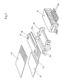
- the connector shown in Fig. 1 has an insulating body formed housing 10, which is attachable to a circuit board 50.
- the housing 10 is spaced apart from one another on one end face Windows 11 and on the opposite side with an opening 12 provided.
- the interior of the housing 10 is in the area of the windows 11 designed as a contact carrier for receiving contact elements 60, whose connection area is led out of the windows 11 in order to Conductor tracks 51 of the circuit board 50 to be electrically connected.
- the contact elements 60 are designed as resilient fork contacts and have as a contact holder 61 hook-shaped on its upper leg 62 Projections on the on the window 11 facing portion of the upper inner surface 15 of the housing 10 are locked, as in Fig. 3a and 4a can be seen.
- Insert element 20 In the opening 12 is an insertion element 20, which has a flat contact surface 21 for a flat cable 40, insertable. Insert element 20 is with a recess extending transversely across the bearing surface 21 22 provided. Guide surfaces are located on both sides of the support surface 21 23 for the flat cable 40 and cams 24, which are on the support surface 21 positioned flat line 40 in recesses 42 present thereon intervene positively. Are on the outside of the guide surfaces 23 two arranged one behind the other in the direction of insertion of the insert element 20 Lugs 25, 26 formed. When inserting insert element 20 in the housing 10, the locking lugs 25, 26 act on both sides of the opening 12 arranged fastening sections 13 together. Through the Latches 25, the insertion element 20 in a first Secured position I locked in the housing 10.
- the guide surfaces 23 come orthogonally extending stop surfaces 29 on the outside of the Insert element 20 are arranged to lie on the housing 10, so that a continuous insertion of the insertion element 20 is excluded.
- the fastening sections 13 are perpendicular to Plug direction of the insert element 20 is resilient, which means the insert element 20 almost without resistance in the Safety position I and end position II can be introduced.
- the connector therefore represents a zero force or ZIF connector.
- Clamping element 30 is arranged pivotably.
- the clamping element 30 is on its side opposite the film hinge 32 with a Provided locking hook 34, which in the case of the insertion element 20 pivoted clamping element 30 on the film hinge 32nd opposite side of the insert element 20 can be locked in place, around the flat line 40 positioned on the support surface 21 between the Fix insert element 20 and the clamping element 30 by clamping.
- On the clamping element 30 is formed a projection 31, which at about Insert element 20 pivoted clamping element 30 into the recess 22 engages.
- the flat line 40 positioned on the support surface 21 becomes hereby also pressed into the recess 22 and into a fold 43 deformed. In this way, high holding forces and a reliable strain relief.
- the clamping element 30 is on its front end in the direction of insertion also provided with an inclined ramp 33 which is parallel to the Projection 31 extends and extends over insert element 20 pivoted clamping element 30 spaced from that on the support surface 21 positioned flat line 40 extends.
- the run-up surface 33 runs when the insertion element 20 is inserted into the Housing 10 shortly before reaching the end position II to one above the Opening 12 of the housing 10 formed insertion slope 14, which the ramp surface 33 between the inner surface 15 and the inside of the Housing 10 located plugging area of the contact elements 60 forces.
- the upper leg 62 of the contact elements 60 in the end position II to an associated insulation-free contact area Core 41 of the electrical line 40 is depressed.
- the electrical contacting of the flat cable 40 Only takes place in the end position II the electrical contacting of the flat cable 40, whereas effective protection against accidental contact is reached as soon as Secure position I is guaranteed.
- the contact elements 60 instruct a curvature 64 on its lower leg 63.
- the bottom of the Insert element 20 corresponds to a curvature 64 trained recess 64a provided.
- the arrangement of the curvature 64 on the leg 63 or the recess 64a on the Insert element 20 is such that in the end position II of the Inserted housing 20 insert 20 a latching Contact elements 60 and insert element 20 takes place, which to a contributes to secure contacting. It is also this way perceptible both acoustically and haptically when the insert element 20 reaches the end position II.
- the connector shown in Fig. 1 is a surface mount Component (SMD) trained and therefore within the so-called "pick-and-place technology" processable.
- SMD surface mount Component
- 1a and 1b are alternative Embodiments shown in which the connection area of the Contact elements 60 has straight or angled contact legs, which in metallized holes in the circuit board 50 are pressed or plugged in and soldered.
- the windows 11 additionally extend on the underside of the housing 10 to a grid dimension corresponding to the respective application to be able to provide.
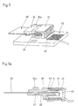
- the embodiment shown in Fig. 2 differs from that 1 only in that the insertion element 20th and the clamping element 30 does not have a film hinge with one another connected, but are formed as separate components.
- the clamping element 30 is provided with recesses 35 into which Insert element 20 correspondingly designed locking hooks 34a on the Insert element 20 arranged clamping element 30 engage, as well 3 and 3a also show such a connector give recognition.
- FIGS. 2a and 4 to 4b is missing another embodiment of a connector, the run-up surface 33.
- the contact surface 21 of the insert element 20 is provided with a the free end of the flat cable 40 receiving and thus an accurate Location of the contact surface between the flat line 40 and the Provide contact elements 60 defining slot 27, as special can be clearly seen in FIGS. 4a and 4b.
- Flat line 40 passed through is on the clamping element 30
- a stop 28 furthermore faces away from the underside of the insertion element 20 educated.
- 5 to 5c are finally different possibilities for Design of the projection 31 and the receiving recess 22 shown.
- several projections 31 can be provided, as can be seen in FIGS. 5b and 5c.
- the projection 31 can over it also be provided with different cross-sectional shapes, for example rectangular as in FIGS. 3a and 4a or triangular as in the aforementioned Characters.
- the recess 22 of the insert element 20 also be different and the respective Use case according to, for example, a continuous opening such as 3a, 4a and 5 or a trough-shaped recess as in the 5a to 5c.
- the connector described above is particularly suitable to be used as a zero force connector.
- the connector is also characterized by high holding forces and a reliable Strain relief.
- it is suitable for both conventional push-through technology as well as for the increasingly widespread SMT.
- Last but not least, it enables the same housing Processing different electrical lines 40 and thus offers also creating jumpers.
Abstract
Description
Die Erfindung betrifft einen Steckverbinder, insbesondere Nullkraft-Steckverbinder, zum Anschließen elektrischer Leitungen an eine Leiterplatte.The invention relates to a connector, in particular zero-force connector, for connecting electrical cables to a printed circuit board.
Steckverbinder sind für eine Vielzahl von Anwendungsmöglichkeiten bekannt. Sie werden daher in den verschiedensten Ausführungsformen und üblicherweise in großen Stückzahlen, beispielsweise im Bereich der sogenannten "braunen Ware", eingesetzt und unterliegen in Hinsicht auf ihre jeweilige Verwendung den unterschiedlichsten Anforderungen. So sind in der Regel neben einer einfachen und kostengünstigen Fertigung, geringen Bauhöhe, großen Haltekräften oder vollautomatischen Montage auch eine Zugentlastung oder zuverlässige Kontaktierung zu erfüllen. Darüber hinaus sind als Nullkraft- oder ZIF-Steckverbinder (Zero Insertion Force) bezeichnete Steckverbinder bekannt, die derart ausgestaltet sein müssen, dass während eines Steck- beziehungsweise Ziehvorganges keine nennenswerten Druck- oder Zugkräfte auftreten.Connectors are for a variety of uses known. They are therefore in a wide variety of embodiments and usually in large quantities, for example in the area of so-called "brown goods", used and subject to their respective use the most diverse requirements. So are in the Usually in addition to simple and inexpensive production, low Height, large holding forces or fully automatic assembly also one Strain relief or reliable contacting. Furthermore are as zero insertion force or ZIF connectors known connectors are known, which must be designed such that none during a plugging or pulling process significant compressive or tensile forces occur.
Im Zusammenhang mit Leiterplatten ist in Hinsicht auf die Ausgestaltung der Steckverbinder grundsätzlich zwischen zwei Verbindungsarten zu differenzieren. Das direkte Stecken, bei dem ein Steckverbinder so auf eine Leiterplatte gesteckt wird, dass die Kontaktelemente des Steckverbinders direkt mit den gedruckten Leiterbahnen einer Leiterplatte kontaktieren werden, und das indirekte Stecken, bei dem ein als zweiteilige Steckverbindung ausgebildeter Steckverbinder eingesetzt wird, dessen eines Teil auf der Leiterplatte montiert und dessen anderes Teil an der elektrischen Leitung angeschlagen wird. Die vorliegende Erfindung zielt zwar primär auf Steckverbinder für das indirekte Stecken ab, lässt sich aber durch geringfügige Modifikationen ohne weiteres auch für das direkte Stecken verwenden, das im allgemeinen eine spezielle Gestaltung der Leiterplatte erfordert.In connection with printed circuit boards, the design of the Connectors basically between two types of connection differentiate. The direct plug-in, in which a connector is so on a Printed circuit board is inserted that the contact elements of the connector Contact directly with the printed conductor tracks of a printed circuit board be, and the indirect plug, in which one as a two-part Plug connection trained connector is used, one of which Part mounted on the circuit board and the other part on the electrical Line is struck. The present invention primarily aims Plug connector for indirect plugging, but can be minor modifications without further ado also for direct insertion use that in general a special design of the circuit board required.
Unter einer Leiterplatte oder Platine werden im Rahmen der vorliegenden Erfindung gedruckte Schaltungen mit Leiterbildern auf einer oder auf beiden Seiten sowie Mehrlagenleiterplatten, sogenannte Multilayer, verstanden. Solche Leiterplatten werden meist mit metallisierten Bohrungen zum Befestigen von Bauelementen mittels Lötverbindungen oder Einpressverbindungen versehen. Die Bauelemente, zum Beispiel der auf der Leiterplatte anzuordnende Teil eines Steckverbinders zum indirekten Stecken, weisen zu diesem Zweck Kontaktelemente auf, die in ihrem leiterplattenseitigen Anschlussbereich als Kontaktbeine, welche in die Bohrungen der Leiterplatte gesteckt werden, ausgebildet sind. Beim Löten, beispielsweise durch Lötverfahren wie dem Schwallöten, werden die Kontaktbeine an der Unterseite der Leiterplatte verlötete, wohingegen beim Einpressen die Kontaktbeine elastisch verformbare oder starre Einpressstifte sind, durch die eine zugleich die mechanische Belastung reduzierende lötfreie elektrische Verbindung hergestellt wird.Under a circuit board or board are within the scope of the present Invention printed circuits with circuit patterns on one or both Sides and multilayer printed circuit boards, so-called multilayer, understood. Such circuit boards are usually with metallized holes Fastening components using solder connections or Provide press-fit connections. The components, for example the one on the Circuit board part of a connector for indirect Plug, have for this purpose contact elements in their PCB-side connection area as contact legs, which in the Bores of the circuit board are inserted, are formed. When soldering, for example by soldering methods such as wave soldering, the Contact legs soldered to the underside of the circuit board, whereas the Press the contact legs into elastically deformable or rigid press-in pins through which the mechanical stress is reduced at the same time solderless electrical connection is established.
Diese sich für die Handbestückung einer Leiterplatte mit Bauelementen regelmäßig gut eignende Durchstecktechnik erfordert verhältnismäßig viel Platz für die Anschlüsse, so dass inzwischen zunehmend die SMT-Technologie (Surface Mounted Technology) Anwendung findet, bei der oberflächenmontierbare Bauelemente, allgemein als SMD (Surface Mounted Devices) bezeichnet, mit lötfähigen Kontaktelementen direkt auf Verbindungsstellen, sogenannten Lötpads, an der Oberfläche der Leiterplatte appliziert werden. Die Lötpads bestehen gewöhnlich aus einer definierten Lötzinnschicht und werden durch Erwärmen der gesamten Einheit, das heißt Leiterplatte bestückt mit den Bauelementen, gelötet. Neben der elektrischen Kontaktierung erfolgt hierdurch auch die mechanische Befestigung, ohne dass es notwendig ist, die Leiterplatte zu durchbohren. Auf diese Weise lassen sich nicht nur kürzere Bestückungszeiten sondern auch erheblich höhere Packungsdichten auf der Leiterplatte und damit eine gemeinhin angestrebte Miniaturisierung erreichen.This is for the manual assembly of a circuit board with components Push-through technology that is regularly suitable requires a great deal Space for the connections, so that meanwhile the SMT technology is increasing (Surface Mounted Technology) is used where surface-mountable components, generally as SMD (Surface Mounted Devices), with solderable contact elements directly on Junctions, so-called solder pads, on the surface of the PCB can be applied. The solder pads usually consist of one defined solder layer and are made by heating the entire Unit, that is, printed circuit board equipped with the components, soldered. In addition to the electrical contacting, this also takes place mechanical attachment without the need to close the circuit board pierce. In this way, not only shorter ones Assembly times but also significantly higher packing densities on the Printed circuit board and thus a commonly sought miniaturization to reach.
Im Stand der Technik sind Steckverbinder zum Anschließen elektrischer Leitungen an eine Leiterplatte bekannt, die ein aus Kunststoff oder Metall bestehendes Gehäuse aufweisen, das in erster Linie dem mechanischen Schutz der Komponenten eines Steckverbinders und der Sicherheit gegen die Berührung elektrischer Teile dient. Je nach Ausgestaltung kann das Gehäuse darüber hinaus für weitere Funktionen, wie etwa einer Verriegelung, Polarisation, Codierung, elektrischen Abschirmung, Dichtung oder einer Zugentlastung, benutzt werden. Als elektrische Leitungen anzusehen sind dabei sowohl eine oder mehrere Adern aufweisende, mit Isolierhüllen, einem Mantel zum Schutz von Aufbauelementen oder Schirmen zur Abschirmung versehene Leitungen, insbesondere flexible Leitungen, Flachleitungen, Schlauchleitungen, geschirmte Leitungen oder Koaxialleitungen, als auch Kabel, die für eine feste Verlegung geeignet sind und einen Mantel aus Kunststoff oder Gummi und gegebenenfalls einen zusätzlichen Mantel aus Metall aufweisen.In the prior art, there are connectors for connecting electrical Lines known to a circuit board, the one made of plastic or metal have existing housing that primarily mechanical Protection of the components of a connector and security against touching electrical parts. Depending on the design, this can Housing also for other functions, such as one Locking, polarization, coding, electrical shielding, sealing or a strain relief. As electrical lines both one or more cores with, are to be seen Insulating sleeves, a jacket to protect structural elements or Shields for shielding cables, especially flexible Cables, flat cables, hose lines, shielded cables or Coaxial lines, as well as cables that are suitable for fixed installation and a jacket made of plastic or rubber and optionally one have additional metal sheath.
Nachteilig bei den bekannten Steckverbindern ist die verhältnismäßig aufwendige Weise, mit der vor allem eine Zugentlastung realisiert wird. Unbefriedigend ist auch die komplizierte und unzuverlässige Kontaktierung der elektrischen Leitungen.The disadvantage of the known connectors is the relative complex way with which a strain relief is realized. The complicated and unreliable contacting is also unsatisfactory of the electrical lines.
Der Erfindung liegt die Aufgabe zugrunde, einen Steckverbinder zum Anschließen elektrischer Leitungen an eine Leiterplatte bereitzustellen, mit dem sich auf vergleichsweise einfache Weise eine verlässliche Zugentlastung und zuverlässige Kontaktierung der elektrischen Leitung erzielen lassen.The invention has for its object to provide a connector for connecting electrical lines to a circuit board, with which a reliable strain relief and reliable contacting of the electrical line can be achieved in a comparatively simple manner.
Diese Aufgabe wird erfindungsgemäß durch einen Steckverbinder der eingangs genannten Art gelöst, der aus einem auf der Leiterplatte befestigbaren Gehäuse, das an einer Stirnseite mit voneinander beabstandeten Fenstern versehen ist und in diesen Bereichen als Kontaktträger zur Aufnahme von Kontaktelementen dient, und einem in eine den Fenstern gegenüberliegende Öffnung des Gehäuses einsteckbaren Einschubelement, das in einer ersten Sicherungsstellung und einer zweiten Endstellung im Gehäuse arretierbar ist und eine die elektrische Leitung positionierende und mit einer Ausnehmung versehene Auflagefläche aufweist, besteht, wobei die elektrische Leitung zwischen der Auflagefläche und einem an dem Einschubelement rastend festlegbaren Klemmelement, an dem wenigstens ein in die Ausnehmung eingreifender Vorsprung angeordnet ist, einklemmbar ist, und wobei das isolationsfreie Ende einer Ader der elektrischen Leitung einen im Gehäuse befindlichen Steckbereich eines einzelnen Kontaktelements in der Endstellung des in das Gehäuse eingeführten Einschubelements kontaktiert und ein aus den Fenstern herausführbarer Anschlussbereich des Kontaktelements mit einer Leiterbahn der Leiterplatte elektrisch leitend verbindbar ist.This object is inventively achieved by a connector of the aforementioned type, consisting of a fastenable on the circuit board housing, which is provided on a front side with spaced windows and serves as a contact carrier for receiving contact elements in these areas, and in one of the windows Opposite opening of the insertable plug-in element, which can be locked in a first securing position and a second end position in the housing and has a support surface that positions the electrical line and has a recess, the electrical line between the support surface and one that can be locked in place on the insert element Clamping element, on which at least one projection engaging in the recess is arranged, can be clamped, and the insulation-free end of a wire of the electrical line has a plug-in area of a single contact located in the housing elements contacted in the end position of the insert element inserted into the housing and a connection area of the contact element which can be led out of the windows can be connected in an electrically conductive manner to a conductor track of the circuit board.
Einem solchen Steckverbinder liegt die Erkenntnis zugrunde, dass sich eine verlässliche Zugentlastung dann erzielen lässt, wenn ein an dem Klemmelement angeordneter Vorsprung in die Ausnehmung des Einschubelements eingreift. Denn auf diese Weise wird der zwischen dem Einschubelement und dem Klemmelement eingeklemmte elektrische Leiter gleichfalls in die Ausnehmung gedrückt und hierdurch zusätzlich formschlüssig fixiert. Zu einer zuverlässigen Kontaktierung der elektrischen Leitung trägt ferner bei, dass das Einschubelement zunächst in einer Sicherungsstellung in dem Gehäuse arretierbar ist, bevor es durch weiteres Einschieben in die Endstellung im Gehäuse gelangt, in der dann die Kontaktelemente kontaktiert werden. Da die Kontaktierung somit erst bei bereits zusammengefügten Einschubelement und Gehäuse stattfindet, ist neben einer gezielten und stets gleichbleibenden Kontaktierung der Kontaktelemente zugleich auch ein wirksamer Berührungsschutz der gegebenenfalls schon mit der Kontaktierung spannungsführenden elektrischen Leitung sichergestellt.Such a connector is based on the knowledge that a reliable strain relief can be achieved if one of the Clamping element arranged projection in the recess of the Insert element engages. Because in this way the between the Insert element and the clamping element clamped electrical conductors also pressed into the recess and thereby additionally positively fixed. For reliable contacting of the electrical Line also contributes to the fact that the insertion element is initially in a Secured position in the housing can be locked before it by another Insert in the end position in the housing, in which the Contact elements are contacted. Because the contacting is only at already inserted insert element and housing takes place in addition to targeted and constant contacting of the Contact elements also an effective protection against accidental contact if necessary, already live with the contact electrical line ensured.
Um die elektrische Leitung bequem auf der Auflagefläche des Einschubelements positionieren zu können, ist es zweckmäßig, das Einschubelement und das Klemmelement als getrennte Bauteile auszubilden oder über ein Filmscharnier miteinander zu verbinden. Nützlich ist außerdem, das Einschubelement beidseitig der Auflagefläche mit Führungsflächen für die elektrische Leitung zu versehen. Eine präzise Positionierung der elektrischen Leitung auf der Auflagefläche lässt sich dadurch gewährleisten. Zu diesem Zweck ist es überdies vorteilhaft, wenn das Einschubelement wenigstens einen Nocken aufweist, der formschlüssig in eine Aussparung der elektrischen Leitung eingreift. Hierdurch lässt sich besonders die Lage des freien Endes der elektrischen Leitung auf dem Einschubelement exakt definieren, so dass das Eindrücken der elektrischen Leitung in die Ausnehmung durch den Vorsprung ohne Einfluss auf die Positionierung der elektrischen Leitung auf der Auflagefläche bleibt. Der oder die Nocken können dabei wahlweise an den Führungsflächen oder an einer beliebigen Stelle auf der Auflagefläche angeordnet sein. Letzteres ist im Allgemeinen jedoch nur bei Inkaufnahme des Verlustes von einer oder mehrerer Adern zu realisieren.To comfortably connect the electrical cable on the contact surface of the To be able to position the insertion element, it is expedient that Insert element and the clamping element as separate components or to connect with each other via a film hinge. Is useful in addition, the insert element on both sides of the support surface To provide guide surfaces for the electrical line. A precise one The electrical cable can be positioned on the support surface thereby guarantee. For this purpose, it is also advantageous if the insert element has at least one cam which is form-fitting engages in a recess of the electrical line. This allows especially the location of the free end of the electrical line on the Define the insert element exactly, so that the impression of the electrical Lead into the recess through the projection without affecting the Positioning of the electrical line on the contact surface remains. The river Oder the cams can either be on the guide surfaces or on a be placed anywhere on the support surface. The latter is in Generally, however, only if the loss of one or to implement multiple wires.
Vorteilhafterweise ist das Einschubelement mit in Steckrichtung hintereinander angeordneten ersten und zweiten Rastnasen versehen, die an einem entsprechend ausgebildeten Befestigungsabschnitt des Gehäuses zum Arretieren des Einschubelements in der Sicherungsstellung und Endstellung festlegbar sind. Dies stellt eine in konstruktiver Hinsicht einfache und damit kostengünstige Ausgestaltung dar. Als vorteilhaft hat sich außerdem herausgestellt, den Befestigungsabschnitt senkrecht zur Steckrichtung des Einschubelements federnd auszubilden. Durch die so erreichte Nachgiebigkeit des Befestigungsabschnitts lässt sich das Einschubelement annähernd widerstandslos in das Gehäuse einstecken und somit ein Nullkraft-Steckverbinder bilden.Advantageously, the insertion element is in the direction of insertion provided first and second locking lugs arranged one behind the other on a correspondingly designed fastening section of the housing for locking the insert element in the securing position and End position can be determined. This makes it structurally simple and thus an inexpensive embodiment. Has proven to be advantageous also highlighted the mounting section perpendicular to To form the insertion direction of the insert element resiliently. Because of that the flexibility of the fastening section can be achieved Insert the insert element into the housing almost without resistance and thus form a zero force connector.
Gemäß einer besonders vorteilhaften Weiterbildung des erfindungsgemäßen Steckverbinders ist das Klemmelement an seiner in Steckrichtung vorderen Stirnseite mit einer schrägen Auflauffläche versehen, die beabstandet zu der Auflagefläche in der Endstellung des Einschubelements den Steckbereich eines Kontaktelements auf die zugehörigen isolationsfreien Adern der elektrischen Leitung niederdrückt. Diese Ausbildung gewährleistet, dass einerseits die Kontaktierung der Kontaktelemente ausschließlich in der Endstellung des Einschubelements erfolgt und andererseits die isolationsfreien Adern der elektrischen Leitung reliabel kontaktiert werden.According to a particularly advantageous development of the invention Connector is the clamping element at its front in the direction of insertion End face with an oblique ramp surface that is spaced from the Support surface in the end position of the insert element, the plug-in area of a contact element on the associated insulation-free wires electrical line. This training ensures that on the one hand the contacting of the contact elements exclusively in the End position of the insert element takes place and on the other hand the insulation-free wires of the electrical line can be contacted reliably.
In einer weiteren vorteilhaften Ausgestaltung des Steckverbinders kann alternativ oder zusätzlich die Auflagefläche mit einem das freie Ende der elektrischen Leitung aufnehmenden Schlitz versehen sein, wobei in der Endstellung des Einschubelements der Steckbereich eines Kontaktelements die zugehörige isolationsfreie Ader der elektrischen Leitung im Bereich des Schlitzes kontaktiert. Bei dieser Ausgestaltung wird durch den Schlitz auf einfache Weise eine genaue Lage der Kontaktfläche zwischen den isolationsfreien Adern der elektrischen Leitung und den Kontaktelementen definiert und damit eine zuverlässige Kontaktierung begünstigt. In Weiterbildung des Steckverbinders wird ferner vorgeschlagen, auf der dem Klemmelement abgewandten Unterseite des Einschubelements einen Anschlag für die durch den Schlitz geführte elektrische Leitung vorzusehen. Durch eine solche Weiterbildung lässt sich gezielt ein Kontaktspiel zwischen den Kontaktelementen und der elektrischen Leitung einstellen. Indem nämlich die Länge des durch den Schlitz hindurchgesteckten Abschnitts der elektrischen Leitung so bemessen wird, dass sich die isolationsfreien Adern der elektrischen Leitung durch das am Anschlag anliegende freie Ende der elektrischen Leitung im Bereich des Schlitzes geringfügig von der Auflagefläche abheben, kann der Abstand zu den Kontaktelementen variiert werden.In a further advantageous embodiment of the connector alternatively or additionally, the contact surface with the free end of the electrical line receiving slot may be provided, in which End position of the insert element of the plug area of a contact element the associated insulation-free wire of the electrical line in the area of Slot contacted. In this embodiment, the slot is on simple way an exact location of the contact surface between the insulation-free wires of the electrical line and the contact elements defined and thus favors a reliable contact. In Training of the connector is also proposed on the Clamping element facing away from the insert element Provide a stop for the electrical line through the slot. Such further training allows a contact game between adjust the contact elements and the electrical cable. By doing namely the length of the section of the electrical cable is dimensioned so that the insulation-free wires the electrical line through the free end of the electrical line in the area of the slot slightly from the Lift off the contact surface, the distance to the contact elements can vary become.
Im Hinblick auf eine verlässliche Zugentlastung und sicheren Formschluss ist es günstig, wenn in Abhängigkeit von der jeweils verwendeten elektrischen Leitung der Vorsprung eine im Querschnitt rechteckige, dreieckige oder gerundete Form aufweist. Die Ausnehmung des Einschubelements kann dabei dem jeweiligen Anwendungsfall angepasst ebenfalls unterschiedlich ausgebildet sein, zum Beispiel als durchgehende Öffnung oder muldenförmige Aussparung. Zweckmäßigerweise sind die Kontaktelemente in ihrem Steckbereich als federnder Gabelkontakt ausgebildet, der eine im wesentlichen hakenförmige Kontakthalterung zum Verrasten im Gehäuse aufweist. Dies ermöglicht bei einfacher Montage eine sichere Befestigung der Kontaktelemente im Gehäuse, und zwar selbst dann, wenn der Anschlussbereich der Kontaktelemente durch die Auflauffläche auf die elektrische Leitung niedergedrückt wird. Zweckmäßig ist daneben, wenn die Kontaktelemente in ihrem Steckbereich einen Schenkel aufweisen, der mit einer Wölbung versehen ist, die in der Endstellung in eine korrespondierend ausgebildete Aussparung am Einschubelement einrastet. Eine solche Ausgestaltung bietet den Vorteil, dass zum einen eine zusätzliche Arretierung des Einschubelements im Gehäuse bewirkt und zum anderen das Erreichen der Endstellung sowohl in akustischer als auch in haptischer Hinsicht angezeigt wird. Die Wölbung kann dabei sowohl konvex als auch konkav an dem Schenkel ausgebildet sein. Im letzteren Fall ist an Stelle der Aussparung ein entsprechend geformter Vorsprung an dem Einschubelement vorzusehen.With regard to a reliable strain relief and a secure form fit it is favorable if depending on the electrical used in each case Conduct the projection a rectangular, triangular or cross section has a rounded shape. The recess of the insert element can adapted to the respective application also different be formed, for example as a continuous opening or trough-shaped recess. The contact elements are expedient formed in their plug-in area as a resilient fork contact, the one in essential hook-shaped contact holder for locking in the housing having. This enables secure attachment with simple assembly the contact elements in the housing, even if the Connection area of the contact elements through the contact surface on the electrical line is depressed. It is useful if the Contact elements in their plug area have a leg that with is provided with a curvature which corresponds to a in the end position trained recess snaps into place. Such Design offers the advantage that an additional one Locking of the insert element in the housing and on the other reaching the end position in both acoustic and haptic Terms is displayed. The curvature can be both convex and be concave on the leg. In the latter case, the Recess a correspondingly shaped projection on the Insert element to be provided.
Je nach Anwendungszweck ist es zudem sinnvoll, die Kontaktelemente in ihrem Anschlussbereich mit geraden oder abgewinkelten Kontaktbeinen zu versehen, die in die Leiterplatte eingepresst oder mit dieser verlötet sind, um bei einem solchen stehenden beziehungsweise liegenden Steckverbinder eine dauerhafte elektrische Verbindung mit der Leiterplatte sicherzustellen. Schließlich wird vorgeschlagen, das Gehäuse als Isolierkörper auszubilden, so dass zusätzliche Mittel, um die einzelnen Kontaktelemente zu isolieren, entbehrlich werden.Depending on the application, it is also useful to put the contact elements in their connection area with straight or angled contact legs provided, which are pressed into the circuit board or soldered to it with such a standing or lying connector ensure a permanent electrical connection to the circuit board. Finally, it is proposed to design the housing as an insulating body, so that additional means to isolate the individual contact elements, become dispensable.
Einzelheiten und weitere Vorteile der Gegenstände der vorliegenden Erfindung ergeben sich aus der nachfolgenden Beschreibung bevorzugter Ausführungsbeispiele. In den zugehörigen Zeichnungen zeigen im Einzelnen:
- Fig. 1
- eine Explosionsdarstellung eines mit einer Flachleitung verbundenen Steckverbinders in einer ersten Ausführungsform;
- Fig. 1a
- eine perspektivische Ansicht eines Steckverbinders in einer zweiten Ausführungsform;
- Fig. 1b
- eine perspektivische Ansicht eines Steckverbinders in einer dritten Ausführungsform;
- Fig. 2
- eine Explosionsdarstellung eines mit einer Flachleitung verbundenen Steckverbinders in einer vierten Ausführungsform;
- Fig. 2a
- eine Explosionsdarstellung eines mit einer Flachleitung verbundenen Steckverbinders in einer fünften Ausführungsform;
- Fig. 3
- eine perspektivische Ansicht des auf einer Leiterplatte angeordneten Steckverbinders nach Fig. 2;
- Fig. 3a
- eine Schnittdarstellung des Steckverbinders nach Fig. 3;
- Fig. 4
- eine perspektivische Ansicht des auf einer Leiterplatte angeordneten Steckverbinders nach Fig. 2a;
- Fig. 4a
- eine Schnittdarstellung des Steckverbinders nach Fig. 4;
- Fig. 4b
- eine perspektivische Ansicht eines Einschubelements des Steckverbinders nach Fig. 4;
- Fig. 5
- eine Schnittdarstellung einer ersten Variante eines auf einem Einschubelement festgelegten Klemmelements im Bereich eines in eine Ausnehmung eingreifenden Vorsprungs;
- Fig. 5a
- eine Schnittdarstellung einer zweiten Variante nach Fig. 5;
- Fig. 5b
- eine Schnittdarstellung einer dritten Variante nach Fig. 5;
- Fig. 5c
- eine Schnittdarstellung einer vierten Variante nach Fig. 5;
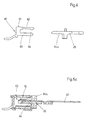
- Fig. 6
- eine Seitenansicht eines Kontaktelements und eines Einschubelements und
- Fig. 6a
- eine das Kontaktelement und das Einschubelement gemäß Fig. 6 in einem verrasteten Zustand abbildende Schnittdarstellung.
- Fig. 1
- an exploded view of a connector connected to a flat cable in a first embodiment;
- Fig. 1a
- a perspective view of a connector in a second embodiment;
- Fig. 1b
- a perspective view of a connector in a third embodiment;
- Fig. 2
- an exploded view of a connector connected to a flat cable in a fourth embodiment;
- Fig. 2a
- an exploded view of a connector connected to a flat cable in a fifth embodiment;
- Fig. 3
- a perspective view of the connector arranged on a circuit board according to FIG. 2;
- Fig. 3a
- a sectional view of the connector of FIG. 3;
- Fig. 4
- a perspective view of the connector arranged on a circuit board according to Fig. 2a;
- Fig. 4a
- a sectional view of the connector of FIG. 4;
- Fig. 4b
- a perspective view of an insertion element of the connector of FIG. 4;
- Fig. 5
- a sectional view of a first variant of a clamping element fixed on an insertion element in the region of a projection engaging in a recess;
- Fig. 5a
- a sectional view of a second variant of FIG. 5;
- Fig. 5b
- a sectional view of a third variant of FIG. 5;
- Fig. 5c
- a sectional view of a fourth variant of FIG. 5;
- Fig. 6
- a side view of a contact element and an insertion element and
- Fig. 6a
- a sectional view depicting the contact element and the insert element according to FIG. 6 in a locked state.
Der in Fig. 1 dargestellte Steckverbinder weist ein als Isolierkörper
ausgebildetes Gehäuse 10 auf, das auf einer Leiterplatte 50 befestigbar ist.
Das Gehäuse 10 ist an einer Stirnseite mit voneinander beabstandeten
Fenstern 11 und an der dieser gegenüberliegenden Seite mit einer Öffnung
12 versehen. Im Bereich der Fenstern 11 ist das Innere des Gehäuses 10
als Kontaktträger zur Aufnahme von Kontaktelementen 60 ausgebildet,
deren Anschlussbereich aus den Fenstern 11 herausgeführt ist, um mit
Leiterbahnen 51 der Leiterplatte 50 elektrisch leitend verbunden zu werden.
Die Kontaktelemente 60 sind als federnder Gabelkontakt ausgebildet und
weisen als Kontakthalterung 61 an ihrem oberen Schenkel 62 hakenförmige
Vorsprünge auf, die an einem den Fenstern 11 zugewandten Abschnitt der
oberen Innenfläche 15 des Gehäuses 10 verrastet werden, wie in Fig. 3a
und 4a zu erkennen ist.The connector shown in Fig. 1 has an insulating body
formed
In die Öffnung 12 ist ein Einschubelement 20, das eine plane Auflagefläche
21 für eine Flachleitung 40 aufweist, einsteckbar. Das Einschubelement 20
ist mit einer sich quer über die Auflagefläche 21 erstreckenden Ausnehmung
22 versehen. Beidseitig der Auflagefläche 21 befinden sich Führungsflächen
23 für die Flachleitung 40 und Nocken 24, die bei auf der Auflagefläche 21
positionierter Flachleitung 40 in an dieser vorhandene Aussparungen 42
formschlüssig eingreifen. Auf der Außenseite der Führungsflächen 23 sind
zwei in Steckrichtung des Einschubelements 20 hintereinander angeordnete
Rastnasen 25, 26 ausgebildet. Beim Einschieben des Einschubelements 20
in das Gehäuse 10 wirken die Rastnasen 25, 26 mit beidseitig der Öffnung
12 angeordneten Befestigungsabschnitten 13 zusammen. Durch die
Rastnasen 25 wird das Einschubelement 20 in einer ersten
Sicherungsstellung I im Gehäuse 10 arretiert. Die Rastnasen 26 hingegen
legen das Einschubelement 20 in einer zweiten Endstellung II am Gehäuse
10 fest. In der Endstellung II kommen orthogonal zu den Führungsflächen 23
verlaufende Anschlagflächen 29, die an der Außenseite des
Einschubelements 20 angeordnet sind, an dem Gehäuse 10 zu liegen, so
dass ein fortgesetztes Einschieben des Einschubelements 20
ausgeschlossen ist. Die Befestigungsabschnitte 13 sind senkrecht zur
Steckrichtung des Einschubelements 20 federnd ausgebildet, wodurch sich
das Einschubelement 20 annähernd widerstandslos in die
Sicherungsstellung I und Endstellung II einführen lässt. Der Steckverbinder
stellt daher einen Nullkraft- oder ZIF-Steckverbinder dar.In the
An dem Einschubelement 20 ist mittels eines Filmscharniers 32 ein
Klemmelement 30 verschwenkbar angeordnet. Das Klemmelement 30 ist an
seiner dem Filmscharnier 32 gegenüberliegenden Seite mit einem
Rasthaken 34 versehen, der bei über das Einschubelement 20
verschwenktem Klemmelement 30 an der dem Filmscharnier 32
gegenüberliegenden Seite des Einschubelements 20 rastend festlegbar ist,
um die auf der Auflagefläche 21 positionierte Flachleitung 40 zwischen dem
Einschubelement 20 und dem Klemmelement 30 klemmend zu fixieren. An
dem Klemmelement 30 ist ein Vorsprung 31 ausgebildet, der bei über das
Einschubelement 20 verschwenktem Klemmelement 30 in die Ausnehmung
22 eingreift. Die auf der Auflagefläche 21 positionierte Flachleitung 40 wird
hierdurch gleichfalls in die Ausnehmung 22 gedrückt und zu einem Falz 43
verformt. Auf diese Weise ergeben sich hohe Haltekräfte und eine
verlässliche Zugentlastung.On the
Das Klemmelement 30 ist an seiner in Steckrichtung vorderen Stirnseite
außerdem mit einer schrägen Auflauffläche 33 versehen, die parallel zu dem
Vorsprung 31 verläuft und sich bei über das Einschubelement 20
verschwenktem Klemmelement 30 beabstandet zu der auf der Auflagefläche
21 positionierten Flachleitung 40 erstreckt. Wie auch in Fig. 3a zu erkennen,
läuft die Auflauffläche 33 beim Einschieben des Einschubelements 20 in das
Gehäuse 10 kurz vor Erreichen der Endstellung II auf eine oberhalb der
Öffnung 12 des Gehäuses 10 ausgebildete Einführschräge 14 auf, welche
die Auflauffläche 33 zwischen der Innenfläche 15 und dem im Inneren des
Gehäuses 10 befindlichen Steckbereich der Kontaktelemente 60 zwängt.
Dies hat zur Folge, dass der obere Schenkel 62 der Kontaktelemente 60 in
der Endstellung II auf eine zugehörige, im Kontaktbereich isolationsfreie
Ader 41 der elektrischen Leitung 40 niedergedrückt wird. Somit erfolgt erst in
der Endstellung II die elektrische Kontaktierung der Flachleitung 40,
wohingegen ein wirksamer Berührungsschutz schon ab Erreichen der
Sicherungsstellung I gewährleistet ist. The clamping
Wie in den Fig. 6 und 6a zu erkennen ist, weisen die Kontaktelemente 60 an
ihrem unteren Schenkel 63 eine Wölbung 64 auf. Die Unterseite des
Einschubelements 20 ist mit einer zu der Wölbung 64 korrespondierend
ausgebildeten Aussparung 64a versehen. Die Anordnung der Wölbung 64
auf dem Schenkel 63 beziehungsweise der Aussparung 64a an dem
Einschubelement 20 ist derart, dass in der Endstellung II des in das
Gehäuse 10 eingeführten Einschubelements 20 eine Verrastung von
Kontaktelementen 60 und Einschubelement 20 stattfindet, die zu einer
sicheren Kontaktierung beiträgt. Darüber hinaus ist es auf diese Weise
sowohl in akustischer als auch in haptischer Hinsicht wahrnehmbar, wenn
das Einschubelement 20 die Endstellung II erreicht.As can be seen in FIGS. 6 and 6a, the
Der in Fig. 1 dargestellte Steckverbinder ist als oberflächenmontierbares
Bauteil (SMD) ausgebildet und damit im Rahmen der sogenannten "Pick-and-place-Technologie"
verarbeitbar. In den Fig. 1a und 1b sind alternative
Ausführungsformen gezeigt, bei denen der Anschlussbereich der
Kontaktelemente 60 gerade oder abgewinkelte Kontaktbeine aufweist, die in
metallisierte Bohrungen der Leiterplatte 50 eingepresst beziehungsweise
eingesteckt und verlötet werden. Bei der Ausführungsform nach Fig. 1b
erstrecken sich die Fenstern 11 zusätzlich auf der Unterseite des Gehäuses
10, um ein dem jeweiligen Anwendungsfall entsprechendes Rastermaß
bereitstellen zu können.The connector shown in Fig. 1 is a surface mount
Component (SMD) trained and therefore within the so-called "pick-and-place technology"
processable. 1a and 1b are alternative
Embodiments shown in which the connection area of the
Die in Fig. 2 gezeigte Ausführungsform unterscheidet sich von dem
Steckverbinder nach Fig. 1 lediglich darin, dass das Einschubelement 20
und das Klemmelement 30 nicht über ein Filmscharnier miteinander
verbunden, sondern als separate Bauteile ausgebildet sind. Um in diesem
Fall das Klemmelement 30 rastend an dem Einschubelement 20 festzulegen,
ist das Klemmelement 30 mit Ausnehmungen 35 versehen, in die an dem
Einschubelement 20 entsprechend ausgebildete Rasthaken 34a bei auf dem
Einschubelement 20 angeordnetem Klemmelement 30 eingreifen, wie auch
die einen solchen Steckverbinder ebenfalls zeigenden Fig. 3 und 3a zu
erkennen geben. The embodiment shown in Fig. 2 differs from that
1 only in that the insertion element 20th
and the clamping
Im Vergleich hierzu fehlt der in den Fig. 2a und 4 bis 4b abgebildeten
weiteren Ausführungsform eines Steckverbinders die Auflauffläche 33.
Stattdessen ist die Auflagefläche 21 des Einschubelements 20 mit einem
das freie Ende der Flachleitung 40 aufnehmenden und damit eine genaue
Lage der Kontaktfläche zwischen der Flachleitung 40 und den
Kontaktelementen 60 definierenden Schlitz 27 versehen, wie besonders
deutlich in den Fig. 4a und 4b zu erkennen ist. Für die durch den Schlitz 27
hindurchgeführte Flachleitung 40 ist auf der dem Klemmelement 30
abgewandten Unterseite des Einschubelements 20 überdies ein Anschlag 28
ausgebildet. Dies hat zur Folge, dass bedingt durch die klemmende
Arretierung der Flachleitung 40 zwischen Einschubelement 20 und
Klemmelement 30 je nach Länge des durch den Schlitz 27
hindurchgesteckten Abschnitts der Flachleitung 40 die isolationsfreien Adern
41 im Bereich des Schlitzes 27 in der Endstellung II etwas von der
Auflagefläche 21 abgehoben sind und damit eine gezielt variierbare
Kontaktfläche für den oberen Schenkel 62 der Kontaktelemente 60 bilden.
Durch die Lage des Schlitzes 27 auf der Auflagefläche 21 lässt sich darüber
hinaus die Kontaktfläche unabhängig von der durch das Zusammenwirken
der Rastnasen 25, 26 mit den Befestigungsabschnitten 13 festgelegten
Endstellung determinieren. Dies kommt zum Beispiel dann zum Tragen,
wenn ohne Veränderung des Gehäuses 10 unterschiedlich ausgebildete
Kontaktelemente 60, etwa wie in den Fig. 1a und 1b gezeigt, Anwendung
finden sollen. Eine universale Ausgestaltung des Einschubelements 20 lässt
sich somit dann erreichen, wenn mehrere Schlitze 27 parallel hintereinander
in der Auflagefläche 21 angeordnet sind.In comparison, the one shown in FIGS. 2a and 4 to 4b is missing
another embodiment of a connector, the run-
In den Fig. 5 bis 5c schließlich sind unterschiedliche Möglichkeiten für die
Gestaltung des Vorsprungs 31 und der diesen aufnehmenden Ausnehmung
22 gezeigt. Im Hinblick auf eine verlässliche Zugentlastung und sicheren
Formschluss können zum Beispiel mehrere Vorsprünge 31 vorgesehen sein,
wie in den Fig. 5b und 5c zu erkennen ist. Der Vorsprung 31 kann darüber
hinaus auch mit unterschiedlichen Querschnittsformen versehen sein, etwa
rechteckig wie in den Fig. 3a und 4a oder dreieckig wie in den vorgenannten
Figuren. Zudem kann die Ausnehmung 22 des Einschubelements 20
ebenfalls unterschiedlich ausgebildet sein und dem jeweiligen
Anwendungsfall entsprechend zum Beispiel eine durchgehende Öffnung wie
in den Fig. 3a, 4a und 5 oder eine muldenförmige Aussparung wie in den
Fig. 5a bis 5c sein.5 to 5c are finally different possibilities for
Design of the
Der zuvor beschriebene Steckverbinder ist in besonderem Maße geeignet,
als Nullkraft-Steckverbinder verwendet zu werden. Neben einer
zuverlässigen Kontaktierung und wirksamem Berührungsschutz zeichnet
sich der Steckverbinder auch durch hohe Haltekräfte und eine reliable
Zugentlastung aus. Je nach Ausgestaltung eignet er sich sowohl für die
herkömmliche Durchstecktechnik als auch für die zunehmend verbreitetere
SMT. Nicht zuletzt ermöglicht er bei ein und demselben Gehäuse die
Verarbeitung unterschiedlicher elektrischer Leitungen 40 und bietet somit
auch die Erstellung von Jumper. The connector described above is particularly suitable
to be used as a zero force connector. In addition to one
reliable contacting and effective protection against accidental contact
the connector is also characterized by high holding forces and a reliable
Strain relief. Depending on the design, it is suitable for both
conventional push-through technology as well as for the increasingly widespread
SMT. Last but not least, it enables the same housing
Processing different
- 1010th
- Gehäusecasing
- 1111
- Fensterwindow
- 1212th
- Öffnungopening
- 1313
- BefestigungsabschnittFastening section
- 1414
- EinführschrägeChamfer
- 1515
- InnenflächeInner surface
- 1616
- EinschubelementInsert element
- 1717th
- AuflageflächeContact surface
- 1818th
- AusnehmungRecess
- 1919th
- FührungsflächeLeadership area
- 2020th
- Nockencam
- 2121
- RastnaseLatch
- 2222
- RastnaseLatch
- 2323
- Schlitzslot
- 2424th
- Anschlagattack
- 2525th
- AnschlagflächeAbutment surface
- 2626
- KlemmelementClamping element
- 2727
- Vorsprunghead Start
- 2828
- FilmscharnierFilm hinge
- 3333
- AuflaufflächeRamp area
- 3434
- RasthakenLocking hook
- 34a34a
- RasthakenLocking hook
- 3535
- AusnehmungRecess
- 3636
- FlachleitungFlat cable
- 3737
- AderVein
- 3838
- AussparungRecess
- 3939
- FalzFold
- 4040
- LeiterplatteCircuit board
- 4141
- LeiterbahnConductor track
- 4242
- KontaktelementContact element
- 4343
- KontakthalterungContact holder
- 4444
- oberer Schenkelupper leg
- 4545
- unterer Schenkellower leg
- 4646
- WölbungBulge
- 64a64a
- AussparungRecess
- II.
- SicherungsstellungSecuring position
- IIII
- EndstellungEnd position
Claims (14)
Applications Claiming Priority (2)
| Application Number | Priority Date | Filing Date | Title |
|---|---|---|---|
| DE20009788U DE20009788U1 (en) | 2000-05-31 | 2000-05-31 | Connector for connecting electrical cables to a Leipterplatte |
| DE20009788U | 2000-05-31 |
Publications (3)
| Publication Number | Publication Date |
|---|---|
| EP1160921A2 true EP1160921A2 (en) | 2001-12-05 |
| EP1160921A3 EP1160921A3 (en) | 2003-01-08 |
| EP1160921B1 EP1160921B1 (en) | 2004-03-31 |
Family
ID=7942282
Family Applications (1)
| Application Number | Title | Priority Date | Filing Date |
|---|---|---|---|
| EP01112515A Expired - Lifetime EP1160921B1 (en) | 2000-05-31 | 2001-05-23 | Connector for connecting wires to a circuit board |
Country Status (2)
| Country | Link |
|---|---|
| EP (1) | EP1160921B1 (en) |
| DE (2) | DE20009788U1 (en) |
Cited By (1)
| Publication number | Priority date | Publication date | Assignee | Title |
|---|---|---|---|---|
| DE102020130750A1 (en) | 2020-11-20 | 2022-05-25 | Huber Automotive Ag | Printed circuit board assembly, method of manufacturing a printed circuit board assembly and control unit |
Families Citing this family (3)
| Publication number | Priority date | Publication date | Assignee | Title |
|---|---|---|---|---|
| DE10125656A1 (en) * | 2001-05-25 | 2002-11-28 | Delphi Tech Inc | strain relief |
| DE10327043A1 (en) * | 2003-06-16 | 2005-01-05 | BSH Bosch und Siemens Hausgeräte GmbH | Strain relief for an electric cable |
| DE102015111675A1 (en) | 2015-07-17 | 2017-01-19 | Wago Verwaltungsgesellschaft Mbh | Connector and deformation tool for this purpose |
Citations (4)
| Publication number | Priority date | Publication date | Assignee | Title |
|---|---|---|---|---|
| US5474468A (en) * | 1992-09-14 | 1995-12-12 | Sumitomo Wiring Systems, Ltd. | Connector |
| US5759060A (en) * | 1996-01-16 | 1998-06-02 | Hon Hai Precision Ind. Co. Ltd. | Insulation displacement contact connector |
| JPH10308245A (en) * | 1997-05-01 | 1998-11-17 | Yazaki Corp | Fixing method and structure for flexible conductor |
| US6062900A (en) * | 1998-11-30 | 2000-05-16 | Hon Hai Precision Ind. Co., Ltd. | ZIF FFC connector having a strain relief |
-
2000
- 2000-05-31 DE DE20009788U patent/DE20009788U1/en not_active Expired - Lifetime
-
2001
- 2001-05-23 EP EP01112515A patent/EP1160921B1/en not_active Expired - Lifetime
- 2001-05-23 DE DE50101813T patent/DE50101813D1/en not_active Expired - Fee Related
Patent Citations (4)
| Publication number | Priority date | Publication date | Assignee | Title |
|---|---|---|---|---|
| US5474468A (en) * | 1992-09-14 | 1995-12-12 | Sumitomo Wiring Systems, Ltd. | Connector |
| US5759060A (en) * | 1996-01-16 | 1998-06-02 | Hon Hai Precision Ind. Co. Ltd. | Insulation displacement contact connector |
| JPH10308245A (en) * | 1997-05-01 | 1998-11-17 | Yazaki Corp | Fixing method and structure for flexible conductor |
| US6062900A (en) * | 1998-11-30 | 2000-05-16 | Hon Hai Precision Ind. Co., Ltd. | ZIF FFC connector having a strain relief |
Non-Patent Citations (1)
| Title |
|---|
| PATENT ABSTRACTS OF JAPAN vol. 1999, no. 02, 26. Februar 1999 (1999-02-26) & JP 10 308245 A (YAZAKI CORP), 17. November 1998 (1998-11-17) & US 6 156 138 A (MOCHIDUKI) 5. Dezember 2000 (2000-12-05) * |
Cited By (1)
| Publication number | Priority date | Publication date | Assignee | Title |
|---|---|---|---|---|
| DE102020130750A1 (en) | 2020-11-20 | 2022-05-25 | Huber Automotive Ag | Printed circuit board assembly, method of manufacturing a printed circuit board assembly and control unit |
Also Published As
| Publication number | Publication date |
|---|---|
| EP1160921A3 (en) | 2003-01-08 |
| EP1160921B1 (en) | 2004-03-31 |
| DE50101813D1 (en) | 2004-05-06 |
| DE20009788U1 (en) | 2000-09-07 |
Similar Documents
| Publication | Publication Date | Title |
|---|---|---|
| DE19736607C1 (en) | PCB socket | |
| DE3544838C2 (en) | ||
| DE60036250T2 (en) | Modular jack connector with filter cartridge and contact for it | |
| DE60003869T2 (en) | Electrical connector | |
| DE202005002902U1 (en) | Electrical connector | |
| DE2130855A1 (en) | Multiple plug connection | |
| DE102008060642B4 (en) | Connector with grounding plate | |
| DE4309039A1 (en) | Junction box for shielded cables, especially for data transmission cables | |
| DE4312091A1 (en) | Plugs for circuit boards | |
| DE2746273C2 (en) | Electrical connector for attaching a plug-in housing to a substrate | |
| EP0735616A2 (en) | Electric connector, especially for circuit boards | |
| EP2091109B1 (en) | Hardened conductor-connector with mass connection | |
| DE60223319T2 (en) | Electrical connector for receiving a plug | |
| DE102006030712B4 (en) | Connectors | |
| DE19726856C1 (en) | Flat-plug for electrical plug-in connections | |
| DE3731413C2 (en) | ||
| EP1160921B1 (en) | Connector for connecting wires to a circuit board | |
| EP1111725B1 (en) | Connector for circuit board | |
| DE2517465C3 (en) | Connectors | |
| DD297283A5 (en) | CONTACT HOUSING WITH CONTACT ELEMENTS FOR BROADCASTING | |
| EP0402739A1 (en) | Device for electrical connecting of sliding electrical assemblies | |
| DE202013104811U1 (en) | Electrical contact device, in particular electrical pressure terminal and / or base strip | |
| DE102019111193B3 (en) | Interface with PCB contact for PCB | |
| DE602004008094T2 (en) | ELECTRICAL CONNECTOR FOR A FLEXIBLE FLAT LEADER AND SWITCHING DEVICE | |
| DE202016002696U1 (en) | Connectors for data transmission |
Legal Events
| Date | Code | Title | Description |
|---|---|---|---|
| PUAI | Public reference made under article 153(3) epc to a published international application that has entered the european phase |
Free format text: ORIGINAL CODE: 0009012 |
|
| AK | Designated contracting states |
Kind code of ref document: A2 Designated state(s): AT BE CH CY DE DK ES FI FR GB GR IE IT LI LU MC NL PT SE TR |
|
| AX | Request for extension of the european patent |
Free format text: AL;LT;LV;MK;RO;SI |
|
| PUAL | Search report despatched |
Free format text: ORIGINAL CODE: 0009013 |
|
| AK | Designated contracting states |
Kind code of ref document: A3 Designated state(s): AT BE CH CY DE DK ES FI FR GB GR IE IT LI LU MC NL PT SE TR |
|
| AX | Request for extension of the european patent |
Free format text: AL;LT;LV;MK;RO;SI |
|
| 17P | Request for examination filed |
Effective date: 20030415 |
|
| 17Q | First examination report despatched |
Effective date: 20030606 |
|
| AKX | Designation fees paid |
Designated state(s): DE FR GB IT |
|
| GRAP | Despatch of communication of intention to grant a patent |
Free format text: ORIGINAL CODE: EPIDOSNIGR1 |
|
| GRAS | Grant fee paid |
Free format text: ORIGINAL CODE: EPIDOSNIGR3 |
|
| GRAA | (expected) grant |
Free format text: ORIGINAL CODE: 0009210 |
|
| AK | Designated contracting states |
Kind code of ref document: B1 Designated state(s): DE FR GB IT |
|
| REG | Reference to a national code |
Ref country code: GB Ref legal event code: FG4D Free format text: NOT ENGLISH |
|
| REG | Reference to a national code |
Ref country code: IE Ref legal event code: FG4D Free format text: GERMAN |
|
| REF | Corresponds to: |
Ref document number: 50101813 Country of ref document: DE Date of ref document: 20040506 Kind code of ref document: P |
|
| GBT | Gb: translation of ep patent filed (gb section 77(6)(a)/1977) |
Effective date: 20040510 |
|
| ET | Fr: translation filed | ||
| REG | Reference to a national code |
Ref country code: IE Ref legal event code: FD4D |
|
| PLBE | No opposition filed within time limit |
Free format text: ORIGINAL CODE: 0009261 |
|
| STAA | Information on the status of an ep patent application or granted ep patent |
Free format text: STATUS: NO OPPOSITION FILED WITHIN TIME LIMIT |
|
| 26N | No opposition filed |
Effective date: 20050104 |
|
| PGFP | Annual fee paid to national office [announced via postgrant information from national office to epo] |
Ref country code: DE Payment date: 20080602 Year of fee payment: 8 |
|
| PGFP | Annual fee paid to national office [announced via postgrant information from national office to epo] |
Ref country code: IT Payment date: 20080523 Year of fee payment: 8 |
|
| PGFP | Annual fee paid to national office [announced via postgrant information from national office to epo] |
Ref country code: GB Payment date: 20080522 Year of fee payment: 8 |
|
| GBPC | Gb: european patent ceased through non-payment of renewal fee |
Effective date: 20090523 |
|
| REG | Reference to a national code |
Ref country code: FR Ref legal event code: ST Effective date: 20100129 |
|
| PG25 | Lapsed in a contracting state [announced via postgrant information from national office to epo] |
Ref country code: FR Free format text: LAPSE BECAUSE OF NON-PAYMENT OF DUE FEES Effective date: 20090602 |
|
| PGFP | Annual fee paid to national office [announced via postgrant information from national office to epo] |
Ref country code: FR Payment date: 20080526 Year of fee payment: 8 |
|
| PG25 | Lapsed in a contracting state [announced via postgrant information from national office to epo] |
Ref country code: GB Free format text: LAPSE BECAUSE OF NON-PAYMENT OF DUE FEES Effective date: 20090523 |
|
| PG25 | Lapsed in a contracting state [announced via postgrant information from national office to epo] |
Ref country code: DE Free format text: LAPSE BECAUSE OF NON-PAYMENT OF DUE FEES Effective date: 20091201 |
|
| PG25 | Lapsed in a contracting state [announced via postgrant information from national office to epo] |
Ref country code: IT Free format text: LAPSE BECAUSE OF NON-PAYMENT OF DUE FEES Effective date: 20090523 |