EP1160616A1 - Liquid crystal display device and method of producing the same - Google Patents
Liquid crystal display device and method of producing the same Download PDFInfo
- Publication number
- EP1160616A1 EP1160616A1 EP01113081A EP01113081A EP1160616A1 EP 1160616 A1 EP1160616 A1 EP 1160616A1 EP 01113081 A EP01113081 A EP 01113081A EP 01113081 A EP01113081 A EP 01113081A EP 1160616 A1 EP1160616 A1 EP 1160616A1
- Authority
- EP
- European Patent Office
- Prior art keywords
- shielding film
- conductive light
- substrate
- liquid crystal
- display device
- Prior art date
- Legal status (The legal status is an assumption and is not a legal conclusion. Google has not performed a legal analysis and makes no representation as to the accuracy of the status listed.)
- Withdrawn
Links
Images


Classifications
-
- G—PHYSICS
- G02—OPTICS
- G02F—OPTICAL DEVICES OR ARRANGEMENTS FOR THE CONTROL OF LIGHT BY MODIFICATION OF THE OPTICAL PROPERTIES OF THE MEDIA OF THE ELEMENTS INVOLVED THEREIN; NON-LINEAR OPTICS; FREQUENCY-CHANGING OF LIGHT; OPTICAL LOGIC ELEMENTS; OPTICAL ANALOGUE/DIGITAL CONVERTERS
- G02F1/00—Devices or arrangements for the control of the intensity, colour, phase, polarisation or direction of light arriving from an independent light source, e.g. switching, gating or modulating; Non-linear optics
- G02F1/01—Devices or arrangements for the control of the intensity, colour, phase, polarisation or direction of light arriving from an independent light source, e.g. switching, gating or modulating; Non-linear optics for the control of the intensity, phase, polarisation or colour
- G02F1/13—Devices or arrangements for the control of the intensity, colour, phase, polarisation or direction of light arriving from an independent light source, e.g. switching, gating or modulating; Non-linear optics for the control of the intensity, phase, polarisation or colour based on liquid crystals, e.g. single liquid crystal display cells
- G02F1/133—Constructional arrangements; Operation of liquid crystal cells; Circuit arrangements
- G02F1/136—Liquid crystal cells structurally associated with a semi-conducting layer or substrate, e.g. cells forming part of an integrated circuit
- G02F1/1362—Active matrix addressed cells
- G02F1/136286—Wiring, e.g. gate line, drain line
-
- G—PHYSICS
- G02—OPTICS
- G02F—OPTICAL DEVICES OR ARRANGEMENTS FOR THE CONTROL OF LIGHT BY MODIFICATION OF THE OPTICAL PROPERTIES OF THE MEDIA OF THE ELEMENTS INVOLVED THEREIN; NON-LINEAR OPTICS; FREQUENCY-CHANGING OF LIGHT; OPTICAL LOGIC ELEMENTS; OPTICAL ANALOGUE/DIGITAL CONVERTERS
- G02F1/00—Devices or arrangements for the control of the intensity, colour, phase, polarisation or direction of light arriving from an independent light source, e.g. switching, gating or modulating; Non-linear optics
- G02F1/01—Devices or arrangements for the control of the intensity, colour, phase, polarisation or direction of light arriving from an independent light source, e.g. switching, gating or modulating; Non-linear optics for the control of the intensity, phase, polarisation or colour
- G02F1/13—Devices or arrangements for the control of the intensity, colour, phase, polarisation or direction of light arriving from an independent light source, e.g. switching, gating or modulating; Non-linear optics for the control of the intensity, phase, polarisation or colour based on liquid crystals, e.g. single liquid crystal display cells
- G02F1/133—Constructional arrangements; Operation of liquid crystal cells; Circuit arrangements
- G02F1/1333—Constructional arrangements; Manufacturing methods
- G02F1/133351—Manufacturing of individual cells out of a plurality of cells, e.g. by dicing
-
- G—PHYSICS
- G02—OPTICS
- G02F—OPTICAL DEVICES OR ARRANGEMENTS FOR THE CONTROL OF LIGHT BY MODIFICATION OF THE OPTICAL PROPERTIES OF THE MEDIA OF THE ELEMENTS INVOLVED THEREIN; NON-LINEAR OPTICS; FREQUENCY-CHANGING OF LIGHT; OPTICAL LOGIC ELEMENTS; OPTICAL ANALOGUE/DIGITAL CONVERTERS
- G02F1/00—Devices or arrangements for the control of the intensity, colour, phase, polarisation or direction of light arriving from an independent light source, e.g. switching, gating or modulating; Non-linear optics
- G02F1/01—Devices or arrangements for the control of the intensity, colour, phase, polarisation or direction of light arriving from an independent light source, e.g. switching, gating or modulating; Non-linear optics for the control of the intensity, phase, polarisation or colour
- G02F1/13—Devices or arrangements for the control of the intensity, colour, phase, polarisation or direction of light arriving from an independent light source, e.g. switching, gating or modulating; Non-linear optics for the control of the intensity, phase, polarisation or colour based on liquid crystals, e.g. single liquid crystal display cells
- G02F1/133—Constructional arrangements; Operation of liquid crystal cells; Circuit arrangements
- G02F1/136—Liquid crystal cells structurally associated with a semi-conducting layer or substrate, e.g. cells forming part of an integrated circuit
- G02F1/1362—Active matrix addressed cells
- G02F1/1368—Active matrix addressed cells in which the switching element is a three-electrode device
-
- G—PHYSICS
- G02—OPTICS
- G02F—OPTICAL DEVICES OR ARRANGEMENTS FOR THE CONTROL OF LIGHT BY MODIFICATION OF THE OPTICAL PROPERTIES OF THE MEDIA OF THE ELEMENTS INVOLVED THEREIN; NON-LINEAR OPTICS; FREQUENCY-CHANGING OF LIGHT; OPTICAL LOGIC ELEMENTS; OPTICAL ANALOGUE/DIGITAL CONVERTERS
- G02F1/00—Devices or arrangements for the control of the intensity, colour, phase, polarisation or direction of light arriving from an independent light source, e.g. switching, gating or modulating; Non-linear optics
- G02F1/01—Devices or arrangements for the control of the intensity, colour, phase, polarisation or direction of light arriving from an independent light source, e.g. switching, gating or modulating; Non-linear optics for the control of the intensity, phase, polarisation or colour
- G02F1/13—Devices or arrangements for the control of the intensity, colour, phase, polarisation or direction of light arriving from an independent light source, e.g. switching, gating or modulating; Non-linear optics for the control of the intensity, phase, polarisation or colour based on liquid crystals, e.g. single liquid crystal display cells
- G02F1/133—Constructional arrangements; Operation of liquid crystal cells; Circuit arrangements
- G02F1/1333—Constructional arrangements; Manufacturing methods
- G02F1/1335—Structural association of cells with optical devices, e.g. polarisers or reflectors
- G02F1/133509—Filters, e.g. light shielding masks
- G02F1/133512—Light shielding layers, e.g. black matrix
-
- G—PHYSICS
- G02—OPTICS
- G02F—OPTICAL DEVICES OR ARRANGEMENTS FOR THE CONTROL OF LIGHT BY MODIFICATION OF THE OPTICAL PROPERTIES OF THE MEDIA OF THE ELEMENTS INVOLVED THEREIN; NON-LINEAR OPTICS; FREQUENCY-CHANGING OF LIGHT; OPTICAL LOGIC ELEMENTS; OPTICAL ANALOGUE/DIGITAL CONVERTERS
- G02F1/00—Devices or arrangements for the control of the intensity, colour, phase, polarisation or direction of light arriving from an independent light source, e.g. switching, gating or modulating; Non-linear optics
- G02F1/01—Devices or arrangements for the control of the intensity, colour, phase, polarisation or direction of light arriving from an independent light source, e.g. switching, gating or modulating; Non-linear optics for the control of the intensity, phase, polarisation or colour
- G02F1/13—Devices or arrangements for the control of the intensity, colour, phase, polarisation or direction of light arriving from an independent light source, e.g. switching, gating or modulating; Non-linear optics for the control of the intensity, phase, polarisation or colour based on liquid crystals, e.g. single liquid crystal display cells
- G02F1/133—Constructional arrangements; Operation of liquid crystal cells; Circuit arrangements
- G02F1/1333—Constructional arrangements; Manufacturing methods
- G02F1/1345—Conductors connecting electrodes to cell terminals
- G02F1/13454—Drivers integrated on the active matrix substrate
-
- G—PHYSICS
- G02—OPTICS
- G02F—OPTICAL DEVICES OR ARRANGEMENTS FOR THE CONTROL OF LIGHT BY MODIFICATION OF THE OPTICAL PROPERTIES OF THE MEDIA OF THE ELEMENTS INVOLVED THEREIN; NON-LINEAR OPTICS; FREQUENCY-CHANGING OF LIGHT; OPTICAL LOGIC ELEMENTS; OPTICAL ANALOGUE/DIGITAL CONVERTERS
- G02F1/00—Devices or arrangements for the control of the intensity, colour, phase, polarisation or direction of light arriving from an independent light source, e.g. switching, gating or modulating; Non-linear optics
- G02F1/01—Devices or arrangements for the control of the intensity, colour, phase, polarisation or direction of light arriving from an independent light source, e.g. switching, gating or modulating; Non-linear optics for the control of the intensity, phase, polarisation or colour
- G02F1/13—Devices or arrangements for the control of the intensity, colour, phase, polarisation or direction of light arriving from an independent light source, e.g. switching, gating or modulating; Non-linear optics for the control of the intensity, phase, polarisation or colour based on liquid crystals, e.g. single liquid crystal display cells
- G02F1/133—Constructional arrangements; Operation of liquid crystal cells; Circuit arrangements
- G02F1/136—Liquid crystal cells structurally associated with a semi-conducting layer or substrate, e.g. cells forming part of an integrated circuit
- G02F1/1362—Active matrix addressed cells
- G02F1/136204—Arrangements to prevent high voltage or static electricity failures
-
- G—PHYSICS
- G02—OPTICS
- G02F—OPTICAL DEVICES OR ARRANGEMENTS FOR THE CONTROL OF LIGHT BY MODIFICATION OF THE OPTICAL PROPERTIES OF THE MEDIA OF THE ELEMENTS INVOLVED THEREIN; NON-LINEAR OPTICS; FREQUENCY-CHANGING OF LIGHT; OPTICAL LOGIC ELEMENTS; OPTICAL ANALOGUE/DIGITAL CONVERTERS
- G02F2202/00—Materials and properties
- G02F2202/22—Antistatic materials or arrangements
Definitions
- the present invention relates to a liquid crystal display device for use as various display devices and a method of producing the same.
- TFT substrates driving substrates
- pixel transistors mounted thereon for constituting a liquid crystal display device are formed en bloc on a substrate (wafer) and individual TFT substrates are obtained by splitting the substrate along scribed lines.
- FIG. 3 is a plan view showing an example of a wiring pattern on such a conventional TFT substrate
- FIG. 4 is a partly sectional view showing an internal laminated structure in the region of line A-A of FIG. 3.
- the region for forming one TFT substrate 10 is demarcated by scribed lines 2 formed in a grating form on a wafer 1, and each TFT substrate 10 is provided with a display region 12 in which pixel transistors 11 are disposed in a matrix form.
- a vertical driving circuit 13 and a horizontal driving circuit 14 for driving each pixel transistor in the display region 12, and, further, on the outside thereof, there are provided a metallic wiring 15 and a plurality of pad portions 16.
- the pad portions 16 are arranged in parallel with and along one side of the display region 12 where the horizontal driving circuit 14 is disposed. These pad portions 16 are connected to the metallic wiring 15, and are brought into contact with terminals of an inspection apparatus or the like. Some of the pad portions 16 are provided as dummies which are not connected to the metallic wiring 15.
- Common electrode portions 15A are provided at corner portions of the metallic wiring 15, for supplying electric power to each of the driving circuits 13, 14 and the like.
- a polycrystalline silicon film 22 is provided on an interlayer insulation film 21 provided on a quartz substrate 20, and an Al electrode film 23 and an upper layer light-shielding film 24 are provided thereon.
- a transparent electrode 26 is provided on the upper side of the upper layer light-shielding film 24, with an interlayer insulation film 25 therebetween.
- Interlayer insulation films 27 and 28 are provided at an outer peripheral portion of the polycrystalline silicon film 22, and have an upwardly projected form, thereby forming the groove of the scribed lines.
- the upper layer light-shielding film 24 is a conductive light-shielding film formed, for example, of an alloy of Al, Ti or the like.
- the transparent electrode 26 is constituted of an ITO film or the like
- the interlayer insulation film 25 is constituted of a P-type TEOS film, a SOG (spin on glass) film or the like.
- the other interlayer insulation films are constituted by appropriately using a silicon oxide film, a silicon nitride film or the like.
- each thin film formed on the scribed lines is removed by dry or wet etching and lithography upon each formation of the thin film.
- the groove of the scribed lines is deepened at the stage of forming the upper-layer light-shielding layer 24, the upper-layer light-shielding layer 24 is left at bottom portions of the scribed lines at the time of processing the upper-layer light-shielding layer 24, and the left portions are exfoliated in cleaning after the processing or the like, leading, for example, to inter-pixel shortcircuit.
- FIG. 4 a structure has been adopted in which the upper-layer light-shielding film is left annularly along the outer peripheral portion of the TFT substrate so that the upper-layer light-shielding film would not easily be exfoliated.
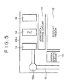
- the upper-layer light-shielding film 24 (shown by solid line 24A in FIG. 5) is disposed also in the vicinity of the above-mentioned pad portions 16, and the presence of such annular upper-layer light shielding film 24 results in that damage due to static electricity is liable to occur in a liquid crystal step.
- the annular upper-layer light-shielding film may be formed at a position away from the pad portions, to thereby prevent the bad influence of static electricity.
- various registration marks and TEG are disposed on the scribed lines, formation of the annular upper-layer light-shielding film at positions away from the center of the TFT substrate along the entire periphery of the TFT substrate results in that it is necessary to widen the scribed lines for providing a layout space.
- chip size is enlarged, and, hence, yield from the TFT substrates is reduced.
- a liquid crystal display device including one of a plurality of driving substrates formed en bloc on a substrate and produced individually by splitting the substrate along scribed lines, the liquid crystal display device including: a conductive light-shielding film formed annularly along a peripheral portion of the driving substrate, and a plurality of pad portions arranged on the inside of the conductive light-shielding film along one side of the driving substrate, wherein the spacing between the conductive light-shielding film and each pad at the side of the driving substrate where the pad portions are provided is at least 10 ⁇ m.
- a method of producing a liquid crystal display device including one of a plurality of driving substrates formed en bloc on a substrate and produced individually by splitting the substrate along scribed lines, the method including: a step of forming a conductive light-shielding film annularly along a peripheral portion of the driving substrate, and a step of forming a plurality of pad portions arranged on the inside of the conductive light-shielding film along one side of the driving substrate, wherein the spacing between the conductive light-shielding film and each pad at the side of the driving substrate where the pad portions are provided is at least 10 ⁇ m.
- the spacing between the conductive light-shielding film and each pad at the side of the driving substrate where the pad portions are provided is at least 10 ⁇ m.
- the spacing of at least 10 ⁇ m has been found to be a value capable of reducing the rate of troubles occurring due to static electricity. Therefore, by setting the spacing between the conductive light-shielding film and each pad to be at least 10 ⁇ m, troubles due to static electricity between the conductive light-shielding film and each pad can be restrained.
- the spacing of at least 10 ⁇ m between the conductive light-shielding film and each pad is provided only at the side of the driving substrate where the pad portions are disposed, the conductive light-shielding film is not spaced away from the center along the entire periphery of the driving substrate, and the desired layout can be realized without much enlarging the chip size.
- the spacing between the conductive light-shielding film and each pad at the side of the driving substrate where the pad portions are provided is set to be at least 10 ⁇ m.
- the spacing of at least 10 ⁇ m between the conductive light-shielding film and each pad is provided only at the side of the driving substrate where the pad portions are provided, the conductive light-shielding film is not spaced away from the center along the entire periphery of the driving substrate, and the desired layout can be realized without much increasing the chip size.
- FIG. 1 is a plan view of major part showing the layout relationship of pad portions and a conductive light-shielding film on a TFT substrate of a liquid crystal display device according to a first embodiment of the present invention.
- the TFT substrates 110 of this embodiment are formed in regions demarcated by scribed lines (omitted in FIG. 1) formed in a grating form on a wafer 101, and a plurality of the TFT substrates 110 are formed en bloc by splitting the wafer 101 along the scribed lines.
- the TFT substrate 110 is provided with a display region 112 in which pixel transistors (omitted in FIG. 1) are disposed in a matrix form at a central area.
- a vertical driving circuit 113 and a horizontal driving circuit 114 for driving each of the pixel transistors in the display region 112 are provided on the outside of the display region 112. Further, a metallic wiring 115 and a plurality of pad portions 116 are provided on the outside of the driving circuits 113 and 114.
- the pad portions 116 are arranged in parallel with and along one side of the display region 112 where the horizontal driving circuit 114 is provided.
- the pad portions 116 are connected to the metallic wiring 115, and are brought into contact with terminals of an inspection apparatus or the like. Some of the pad portions 116 are provided as dummies which are not connected to the metallic wiring 115.
- Common electrode portions 115A are provided at corner portions of the metallic wiring 115, whereby electric power is supplied to each of the driving circuits 113, 114 and the like.
- a conductive light-shielding film 124 is provided on the outside of the metallic wiring 115 and the pad portions 116.
- the conductive light-shielding film 124 is formed in a tetragonal annular shape along the outer periphery of the TFT substrate 110, and is left in the annular form along the outer periphery of the TFT substrate 110 to ensure that, when an upper-layer light-shielding film is formed on the TFT substrate 110, the upper-layer light-shielding film on the side of the scribed lines would not easily be exfoliated at the time of etching or cleaning.
- the conductive light-shielding film 124 can be formed in a thickness of 50 to 500 nm by use of a combination of W, Mo, Ta, Cr, Ti, Al, Cu, Zn, silicides of these elements and alloys of these elements.
- the conductive light-shielding film 124 has a low resistance of not more than 200 K ⁇ / ⁇ , and has a transmittance to at least light in the range of 400 to 500 nm of not more than 10%.
- the position of the conductive light-shielding film 124A disposed on the outside of the pad portions 116 is shifted outwards by 147 nm as compared with the prior art (shown by broken line 24B in FIG. 1) shown in FIG. 5, whereby the spacing between the conductive light-shielding film 124A and the pad portions 116 is set to be, for example, not less than 10 ⁇ m.
- the position and shape of the scribed line are also set according to the conductive light-shielding film 124, 124A.
- films of Al, TiON and Ti are sequentially formed in thicknesses of 100 nm, 50 nm and 100 nm, and are patterned by etching and the like, whereby a belt-like pattern with a width of 6 ⁇ m in plan view is formed.
- a film of P-TEOS is provided in a thickness of 100 nm, then a film of SOG is provided in a thickness of 400 nm to form an interlayer insulation film, a contact hole is opened, and transparent pixel electrodes consisting of an ITO film with a thickness of 70 nm are formed.
- the conductive light-shielding film 124A in the range where the PAD portions 116 are arranged is spaced apart from the PAD portions 116
- the conductive light-shielding film 124A along the side where the PAD portions 116 are arranged may be entirely spaced apart from the PAD portions 116.
- the conductive light-shielding film may be formed at a position largely retracted from the PAD portions so that the conductive light-shielding film is also cut away when the TFT substrates are separated from the wafer at the scribed lines.
- the conductive light-shielding film is absent in the vicinity of the pad portions at the time of press bonding between the pad portions and the flexible substrate, so that the possibility of shortcicuit between the PAD substrate and the flexible substrate due to static electricity can be reduced more assuredly.
- the spacing is set to be not less than 10 ⁇ m, with a more preferable range of the spacing being 150 to 200 ⁇ m.
- the conductive light-shielding film is a cause of capacitance of coupling with adjacent wiring
- the conductive light-shielding film preferably has a low resistance of not more than 100 K ⁇ / ⁇ , more preferably not more than 10 K ⁇ / ⁇ .
Landscapes
- Physics & Mathematics (AREA)
- Nonlinear Science (AREA)
- Mathematical Physics (AREA)
- Chemical & Material Sciences (AREA)
- Crystallography & Structural Chemistry (AREA)
- General Physics & Mathematics (AREA)
- Optics & Photonics (AREA)
- Engineering & Computer Science (AREA)
- Liquid Crystal (AREA)
- Manufacturing & Machinery (AREA)
- Microelectronics & Electronic Packaging (AREA)
- Devices For Indicating Variable Information By Combining Individual Elements (AREA)
Abstract
Description
Claims (8)
- A liquid crystal display device comprising one of a plurality of driving substrates formed en bloc on a substrate and produced individually by splitting said substrate along scribed lines, said liquid crystal display device comprising:a conductive light-shielding film formed annularly along a peripheral portion of said driving substrate, anda plurality of pad portions arranged on the inside of said conductive light-shielding film along one side of said driving substrate, whereinthe spacing between said conductive light-shielding film and each said pad at the side of said driving substrate where said pad portions are provided is at least 10 µm.
- A liquid crystal display device as set forth in claim 1, wherein said conductive light-shielding film is formed by use of a combination of W, Mo, Ta, Cr, Ti, Al, Cu, Zn, silicides of these elements and alloys of these elements.
- A liquid crystal display device as set forth in claim 1, wherein said conductive light-shielding film has a thickness of 50 to 500 nm.
- A liquid crystal display device as set forth in claim 1, wherein said conductive light-shielding film has a low resistance of not more than 200 KΩ/□.
- A liquid crystal display device as set forth in claim 1, wherein said conductive light-shielding film has a transmittance to at least light in the range of 400 to 500 nm of not more than 10%.
- A method of producing a liquid crystal display device comprising one of a plurality of driving substrates formed en bloc on a substrate and produced individually by splitting said substrate along scribed lines, said method comprising:a step of forming a conductive light-shielding film annularly along a peripheral portion of said driving substrate, anda step of forming a plurality of pad portions arranged on the inside of said conductive light-shielding film along one side of said driving substrate, whereinthe spacing between said conductive light-shielding film and each said pad at the side of said driving substrate where said pad portions are provided is at least 10 µm.
- A method of producing a liquid crystal display device as set forth in claim 6, wherein said conductive light-shielding film is formed at the same time when a wiring for pixel transistors or a peripheral driving circuit is formed or when a light-shielding thin film is formed, and is patterned at the same time when said wiring or said light-shielding thin film is patterned.
- A method of producing a liquid crystal display device as set forth in claim 6, wherein said conductive light-shielding film is present on said substrate only when said substrate is processed, and is removed when said driving substrates are split.
Applications Claiming Priority (2)
| Application Number | Priority Date | Filing Date | Title |
|---|---|---|---|
| JP2000162775A JP2001343663A (en) | 2000-05-31 | 2000-05-31 | Liquid crystal display device and manufacturing method thereof |
| JP2000162775 | 2000-05-31 |
Publications (1)
| Publication Number | Publication Date |
|---|---|
| EP1160616A1 true EP1160616A1 (en) | 2001-12-05 |
Family
ID=18666633
Family Applications (1)
| Application Number | Title | Priority Date | Filing Date |
|---|---|---|---|
| EP01113081A Withdrawn EP1160616A1 (en) | 2000-05-31 | 2001-05-29 | Liquid crystal display device and method of producing the same |
Country Status (4)
| Country | Link |
|---|---|
| US (1) | US6441876B1 (en) |
| EP (1) | EP1160616A1 (en) |
| JP (1) | JP2001343663A (en) |
| KR (1) | KR100762113B1 (en) |
Cited By (1)
| Publication number | Priority date | Publication date | Assignee | Title |
|---|---|---|---|---|
| CN103376607A (en) * | 2012-04-12 | 2013-10-30 | 株式会社日本显示器中部 | Liquid crystal display device and method of manufacturing the same |
Families Citing this family (6)
| Publication number | Priority date | Publication date | Assignee | Title |
|---|---|---|---|---|
| JP2004301934A (en) * | 2003-03-28 | 2004-10-28 | Toshiba Matsushita Display Technology Co Ltd | Manufacturing method of liquid crystal display |
| US7365494B2 (en) * | 2004-12-03 | 2008-04-29 | Semiconductor Energy Laboratory Co., Ltd. | Display device and manufacturing method thereof |
| CN100437236C (en) * | 2005-10-28 | 2008-11-26 | 友达光电股份有限公司 | Liquid crystal display panel and circuit layout thereon |
| KR101424784B1 (en) | 2006-01-10 | 2014-07-31 | 가부시키가이샤 한도오따이 에네루기 켄큐쇼 | Display device and manufacturing method thereof |
| JP2008164787A (en) | 2006-12-27 | 2008-07-17 | Epson Imaging Devices Corp | Liquid crystal display device |
| JP2012208301A (en) * | 2011-03-29 | 2012-10-25 | Seiko Epson Corp | Liquid crystal device and projection type display device |
Citations (5)
| Publication number | Priority date | Publication date | Assignee | Title |
|---|---|---|---|---|
| JPH0950044A (en) * | 1995-08-08 | 1997-02-18 | Sony Corp | Active matrix display device |
| EP0793135A1 (en) * | 1994-11-08 | 1997-09-03 | Citizen Watch Co. Ltd. | Liquid crystal display |
| US5739880A (en) * | 1995-12-01 | 1998-04-14 | Hitachi, Ltd. | Liquid crystal display device having a shielding film for shielding light from a light source |
| US5851411A (en) * | 1996-07-09 | 1998-12-22 | Lg Electronics, Inc. | High-density liquid crystal display and method |
| WO1999039239A1 (en) * | 1998-01-30 | 1999-08-05 | Seiko Epson Corporation | Electrooptic device, electronic apparatus using it and method of producing the electrooptic device |
Family Cites Families (3)
| Publication number | Priority date | Publication date | Assignee | Title |
|---|---|---|---|---|
| US6011607A (en) * | 1995-02-15 | 2000-01-04 | Semiconductor Energy Laboratory Co., | Active matrix display with sealing material |
| JP4067588B2 (en) * | 1995-12-19 | 2008-03-26 | 株式会社半導体エネルギー研究所 | Method for manufacturing liquid crystal display device |
| JP3873478B2 (en) * | 1997-12-25 | 2007-01-24 | セイコーエプソン株式会社 | Liquid crystal display device, electronic device, and method of manufacturing liquid crystal display device |
-
2000
- 2000-05-31 JP JP2000162775A patent/JP2001343663A/en active Pending
-
2001
- 2001-05-29 EP EP01113081A patent/EP1160616A1/en not_active Withdrawn
- 2001-05-30 KR KR1020010029959A patent/KR100762113B1/en not_active Expired - Fee Related
- 2001-05-31 US US09/871,122 patent/US6441876B1/en not_active Expired - Lifetime
Patent Citations (6)
| Publication number | Priority date | Publication date | Assignee | Title |
|---|---|---|---|---|
| EP0793135A1 (en) * | 1994-11-08 | 1997-09-03 | Citizen Watch Co. Ltd. | Liquid crystal display |
| JPH0950044A (en) * | 1995-08-08 | 1997-02-18 | Sony Corp | Active matrix display device |
| US5739880A (en) * | 1995-12-01 | 1998-04-14 | Hitachi, Ltd. | Liquid crystal display device having a shielding film for shielding light from a light source |
| US5851411A (en) * | 1996-07-09 | 1998-12-22 | Lg Electronics, Inc. | High-density liquid crystal display and method |
| WO1999039239A1 (en) * | 1998-01-30 | 1999-08-05 | Seiko Epson Corporation | Electrooptic device, electronic apparatus using it and method of producing the electrooptic device |
| US6259505B1 (en) * | 1998-01-30 | 2001-07-10 | Seiko Epson Corporation | Electro-optic apparatus, electronic apparatus therewith, and manufacturing method therefor |
Non-Patent Citations (1)
| Title |
|---|
| PATENT ABSTRACTS OF JAPAN vol. 1997, no. 06 30 June 1997 (1997-06-30) * |
Cited By (3)
| Publication number | Priority date | Publication date | Assignee | Title |
|---|---|---|---|---|
| CN103376607A (en) * | 2012-04-12 | 2013-10-30 | 株式会社日本显示器中部 | Liquid crystal display device and method of manufacturing the same |
| US9329446B2 (en) | 2012-04-12 | 2016-05-03 | Japan Display Inc. | Liquid crystal display device and method of manufacturing the same |
| CN103376607B (en) * | 2012-04-12 | 2016-08-03 | 株式会社日本显示器 | Liquid crystal display and manufacture method thereof |
Also Published As
| Publication number | Publication date |
|---|---|
| KR100762113B1 (en) | 2007-10-02 |
| US20020044237A1 (en) | 2002-04-18 |
| US6441876B1 (en) | 2002-08-27 |
| JP2001343663A (en) | 2001-12-14 |
| KR20010109166A (en) | 2001-12-08 |
Similar Documents
| Publication | Publication Date | Title |
|---|---|---|
| US6734940B2 (en) | Semiconductor device, electro-optical device substrate, liquid crystal device substrate and manufacturing method therefor, liquid crystal device, and projection liquid crystal display device and electronic apparatus using the liquid crystal device | |
| US8772780B2 (en) | Array substrate structure of display panel and method of making the same | |
| US7649586B2 (en) | Display device with floating transistor elements on alternating data lines | |
| US6956626B2 (en) | Thin film transistor liquid crystal display structure | |
| JP5000650B2 (en) | TFT substrate, display panel including the same, display device, and method for manufacturing TFT substrate | |
| US6678017B1 (en) | Display panel and method of fabricating the same | |
| US7863616B2 (en) | Structure of thin film transistor array | |
| JP2006235134A (en) | Liquid crystal display device and manufacturing method thereof | |
| US7872698B2 (en) | Liquid crystal display with structure resistant to exfoliation during fabrication | |
| JPH01123475A (en) | Liquid crystal display equipment | |
| US6441876B1 (en) | Liquid crystal display device and method of producing the same | |
| TWI459477B (en) | Pixel structure and its making method | |
| US6972819B2 (en) | Method of manufacturing IPS-LCD using 4-mask process | |
| US7119411B2 (en) | Interconnect structure for TFT-array substrate and method for fabricating the same | |
| JP4017754B2 (en) | Liquid crystal display device and manufacturing method thereof | |
| JP2004318076A (en) | Method for manufacturing lateral electric field driven liquid crystal display | |
| JP2002111001A (en) | Wiring board and method of manufacturing wiring board | |
| JP4245850B2 (en) | Manufacturing method of electronic device | |
| CN118471984B (en) | Array substrate and display panel | |
| US20060054889A1 (en) | Thin film transistor array panel | |
| KR101399200B1 (en) | Liquid crystal display device and method of manufacturing the same | |
| JP3873164B2 (en) | Manufacturing method of active matrix type liquid crystal display panel | |
| KR20110039123A (en) | LCD and its manufacturing method | |
| JPH03129325A (en) | Manufacture of thin film integrated circuit | |
| JP2000349291A (en) | Thin film transistor array and method of manufacturing thin film transistor array |
Legal Events
| Date | Code | Title | Description |
|---|---|---|---|
| PUAI | Public reference made under article 153(3) epc to a published international application that has entered the european phase |
Free format text: ORIGINAL CODE: 0009012 |
|
| AK | Designated contracting states |
Kind code of ref document: A1 Designated state(s): DE GB NL Kind code of ref document: A1 Designated state(s): AT BE CH CY DE DK ES FI FR GB GR IE IT LI LU MC NL PT SE TR |
|
| AX | Request for extension of the european patent |
Free format text: AL;LT;LV;MK;RO;SI |
|
| 17P | Request for examination filed |
Effective date: 20020506 |
|
| AKX | Designation fees paid |
Free format text: DE GB NL |
|
| 17Q | First examination report despatched |
Effective date: 20040604 |
|
| STAA | Information on the status of an ep patent application or granted ep patent |
Free format text: STATUS: THE APPLICATION IS DEEMED TO BE WITHDRAWN |
|
| 18D | Application deemed to be withdrawn |
Effective date: 20041015 |