EP1158483A2 - Solid-state display with reference pixel - Google Patents
Solid-state display with reference pixel Download PDFInfo
- Publication number
- EP1158483A2 EP1158483A2 EP01201792A EP01201792A EP1158483A2 EP 1158483 A2 EP1158483 A2 EP 1158483A2 EP 01201792 A EP01201792 A EP 01201792A EP 01201792 A EP01201792 A EP 01201792A EP 1158483 A2 EP1158483 A2 EP 1158483A2
- Authority
- EP
- European Patent Office
- Prior art keywords
- pixels
- reference pixel
- display
- pixel
- display device
- Prior art date
- Legal status (The legal status is an assumption and is not a legal conclusion. Google has not performed a legal analysis and makes no representation as to the accuracy of the status listed.)
- Withdrawn
Links
- 238000005259 measurement Methods 0.000 claims abstract description 37
- 239000000758 substrate Substances 0.000 claims abstract description 21
- 238000004458 analytical method Methods 0.000 claims abstract description 20
- 230000004044 response Effects 0.000 claims abstract description 12
- 238000000034 method Methods 0.000 claims description 27
- 230000008859 change Effects 0.000 claims description 7
- 239000003086 colorant Substances 0.000 claims description 4
- 230000032683 aging Effects 0.000 claims description 3
- 239000000463 material Substances 0.000 description 6
- 230000007246 mechanism Effects 0.000 description 6
- 238000013459 approach Methods 0.000 description 5
- 238000005516 engineering process Methods 0.000 description 5
- 238000004519 manufacturing process Methods 0.000 description 5
- 230000001276 controlling effect Effects 0.000 description 4
- 230000000694 effects Effects 0.000 description 4
- 238000010586 diagram Methods 0.000 description 3
- 230000010354 integration Effects 0.000 description 3
- 230000008901 benefit Effects 0.000 description 2
- 238000013461 design Methods 0.000 description 2
- 239000002210 silicon-based material Substances 0.000 description 2
- XUIMIQQOPSSXEZ-UHFFFAOYSA-N Silicon Chemical compound [Si] XUIMIQQOPSSXEZ-UHFFFAOYSA-N 0.000 description 1
- 229910000831 Steel Inorganic materials 0.000 description 1
- 230000001668 ameliorated effect Effects 0.000 description 1
- 230000003542 behavioural effect Effects 0.000 description 1
- 238000012937 correction Methods 0.000 description 1
- 239000013078 crystal Substances 0.000 description 1
- 238000013500 data storage Methods 0.000 description 1
- 230000008713 feedback mechanism Effects 0.000 description 1
- 230000002431 foraging effect Effects 0.000 description 1
- 239000011521 glass Substances 0.000 description 1
- 238000003384 imaging method Methods 0.000 description 1
- 239000012535 impurity Substances 0.000 description 1
- 239000004973 liquid crystal related substance Substances 0.000 description 1
- 230000001404 mediated effect Effects 0.000 description 1
- 239000011368 organic material Substances 0.000 description 1
- 230000002688 persistence Effects 0.000 description 1
- 230000008569 process Effects 0.000 description 1
- 230000001105 regulatory effect Effects 0.000 description 1
- 229910052710 silicon Inorganic materials 0.000 description 1
- 239000010703 silicon Substances 0.000 description 1
- 150000003384 small molecules Chemical class 0.000 description 1
- 239000010959 steel Substances 0.000 description 1
Images

Classifications
-
- G—PHYSICS
- G09—EDUCATION; CRYPTOGRAPHY; DISPLAY; ADVERTISING; SEALS
- G09G—ARRANGEMENTS OR CIRCUITS FOR CONTROL OF INDICATING DEVICES USING STATIC MEANS TO PRESENT VARIABLE INFORMATION
- G09G3/00—Control arrangements or circuits, of interest only in connection with visual indicators other than cathode-ray tubes
- G09G3/20—Control arrangements or circuits, of interest only in connection with visual indicators other than cathode-ray tubes for presentation of an assembly of a number of characters, e.g. a page, by composing the assembly by combination of individual elements arranged in a matrix no fixed position being assigned to or needed to be assigned to the individual characters or partial characters
- G09G3/22—Control arrangements or circuits, of interest only in connection with visual indicators other than cathode-ray tubes for presentation of an assembly of a number of characters, e.g. a page, by composing the assembly by combination of individual elements arranged in a matrix no fixed position being assigned to or needed to be assigned to the individual characters or partial characters using controlled light sources
- G09G3/30—Control arrangements or circuits, of interest only in connection with visual indicators other than cathode-ray tubes for presentation of an assembly of a number of characters, e.g. a page, by composing the assembly by combination of individual elements arranged in a matrix no fixed position being assigned to or needed to be assigned to the individual characters or partial characters using controlled light sources using electroluminescent panels
- G09G3/32—Control arrangements or circuits, of interest only in connection with visual indicators other than cathode-ray tubes for presentation of an assembly of a number of characters, e.g. a page, by composing the assembly by combination of individual elements arranged in a matrix no fixed position being assigned to or needed to be assigned to the individual characters or partial characters using controlled light sources using electroluminescent panels semiconductive, e.g. using light-emitting diodes [LED]
- G09G3/3208—Control arrangements or circuits, of interest only in connection with visual indicators other than cathode-ray tubes for presentation of an assembly of a number of characters, e.g. a page, by composing the assembly by combination of individual elements arranged in a matrix no fixed position being assigned to or needed to be assigned to the individual characters or partial characters using controlled light sources using electroluminescent panels semiconductive, e.g. using light-emitting diodes [LED] organic, e.g. using organic light-emitting diodes [OLED]
- G09G3/3225—Control arrangements or circuits, of interest only in connection with visual indicators other than cathode-ray tubes for presentation of an assembly of a number of characters, e.g. a page, by composing the assembly by combination of individual elements arranged in a matrix no fixed position being assigned to or needed to be assigned to the individual characters or partial characters using controlled light sources using electroluminescent panels semiconductive, e.g. using light-emitting diodes [LED] organic, e.g. using organic light-emitting diodes [OLED] using an active matrix
-
- G—PHYSICS
- G09—EDUCATION; CRYPTOGRAPHY; DISPLAY; ADVERTISING; SEALS
- G09G—ARRANGEMENTS OR CIRCUITS FOR CONTROL OF INDICATING DEVICES USING STATIC MEANS TO PRESENT VARIABLE INFORMATION
- G09G3/00—Control arrangements or circuits, of interest only in connection with visual indicators other than cathode-ray tubes
- G09G3/20—Control arrangements or circuits, of interest only in connection with visual indicators other than cathode-ray tubes for presentation of an assembly of a number of characters, e.g. a page, by composing the assembly by combination of individual elements arranged in a matrix no fixed position being assigned to or needed to be assigned to the individual characters or partial characters
- G09G3/22—Control arrangements or circuits, of interest only in connection with visual indicators other than cathode-ray tubes for presentation of an assembly of a number of characters, e.g. a page, by composing the assembly by combination of individual elements arranged in a matrix no fixed position being assigned to or needed to be assigned to the individual characters or partial characters using controlled light sources
- G09G3/30—Control arrangements or circuits, of interest only in connection with visual indicators other than cathode-ray tubes for presentation of an assembly of a number of characters, e.g. a page, by composing the assembly by combination of individual elements arranged in a matrix no fixed position being assigned to or needed to be assigned to the individual characters or partial characters using controlled light sources using electroluminescent panels
- G09G3/32—Control arrangements or circuits, of interest only in connection with visual indicators other than cathode-ray tubes for presentation of an assembly of a number of characters, e.g. a page, by composing the assembly by combination of individual elements arranged in a matrix no fixed position being assigned to or needed to be assigned to the individual characters or partial characters using controlled light sources using electroluminescent panels semiconductive, e.g. using light-emitting diodes [LED]
- G09G3/3208—Control arrangements or circuits, of interest only in connection with visual indicators other than cathode-ray tubes for presentation of an assembly of a number of characters, e.g. a page, by composing the assembly by combination of individual elements arranged in a matrix no fixed position being assigned to or needed to be assigned to the individual characters or partial characters using controlled light sources using electroluminescent panels semiconductive, e.g. using light-emitting diodes [LED] organic, e.g. using organic light-emitting diodes [OLED]
- G09G3/3225—Control arrangements or circuits, of interest only in connection with visual indicators other than cathode-ray tubes for presentation of an assembly of a number of characters, e.g. a page, by composing the assembly by combination of individual elements arranged in a matrix no fixed position being assigned to or needed to be assigned to the individual characters or partial characters using controlled light sources using electroluminescent panels semiconductive, e.g. using light-emitting diodes [LED] organic, e.g. using organic light-emitting diodes [OLED] using an active matrix
- G09G3/3258—Control arrangements or circuits, of interest only in connection with visual indicators other than cathode-ray tubes for presentation of an assembly of a number of characters, e.g. a page, by composing the assembly by combination of individual elements arranged in a matrix no fixed position being assigned to or needed to be assigned to the individual characters or partial characters using controlled light sources using electroluminescent panels semiconductive, e.g. using light-emitting diodes [LED] organic, e.g. using organic light-emitting diodes [OLED] using an active matrix with pixel circuitry controlling the voltage across the light-emitting element
-
- G—PHYSICS
- G09—EDUCATION; CRYPTOGRAPHY; DISPLAY; ADVERTISING; SEALS
- G09G—ARRANGEMENTS OR CIRCUITS FOR CONTROL OF INDICATING DEVICES USING STATIC MEANS TO PRESENT VARIABLE INFORMATION
- G09G2300/00—Aspects of the constitution of display devices
- G09G2300/04—Structural and physical details of display devices
- G09G2300/0439—Pixel structures
- G09G2300/0465—Improved aperture ratio, e.g. by size reduction of the pixel circuit, e.g. for improving the pixel density or the maximum displayable luminance or brightness
-
- G—PHYSICS
- G09—EDUCATION; CRYPTOGRAPHY; DISPLAY; ADVERTISING; SEALS
- G09G—ARRANGEMENTS OR CIRCUITS FOR CONTROL OF INDICATING DEVICES USING STATIC MEANS TO PRESENT VARIABLE INFORMATION
- G09G2320/00—Control of display operating conditions
- G09G2320/02—Improving the quality of display appearance
- G09G2320/029—Improving the quality of display appearance by monitoring one or more pixels in the display panel, e.g. by monitoring a fixed reference pixel
-
- G—PHYSICS
- G09—EDUCATION; CRYPTOGRAPHY; DISPLAY; ADVERTISING; SEALS
- G09G—ARRANGEMENTS OR CIRCUITS FOR CONTROL OF INDICATING DEVICES USING STATIC MEANS TO PRESENT VARIABLE INFORMATION
- G09G2320/00—Control of display operating conditions
- G09G2320/04—Maintaining the quality of display appearance
- G09G2320/043—Preventing or counteracting the effects of ageing
-
- G—PHYSICS
- G09—EDUCATION; CRYPTOGRAPHY; DISPLAY; ADVERTISING; SEALS
- G09G—ARRANGEMENTS OR CIRCUITS FOR CONTROL OF INDICATING DEVICES USING STATIC MEANS TO PRESENT VARIABLE INFORMATION
- G09G2320/00—Control of display operating conditions
- G09G2320/06—Adjustment of display parameters
- G09G2320/0626—Adjustment of display parameters for control of overall brightness
-
- G—PHYSICS
- G09—EDUCATION; CRYPTOGRAPHY; DISPLAY; ADVERTISING; SEALS
- G09G—ARRANGEMENTS OR CIRCUITS FOR CONTROL OF INDICATING DEVICES USING STATIC MEANS TO PRESENT VARIABLE INFORMATION
- G09G2360/00—Aspects of the architecture of display systems
- G09G2360/14—Detecting light within display terminals, e.g. using a single or a plurality of photosensors
-
- G—PHYSICS
- G09—EDUCATION; CRYPTOGRAPHY; DISPLAY; ADVERTISING; SEALS
- G09G—ARRANGEMENTS OR CIRCUITS FOR CONTROL OF INDICATING DEVICES USING STATIC MEANS TO PRESENT VARIABLE INFORMATION
- G09G2360/00—Aspects of the architecture of display systems
- G09G2360/14—Detecting light within display terminals, e.g. using a single or a plurality of photosensors
- G09G2360/145—Detecting light within display terminals, e.g. using a single or a plurality of photosensors the light originating from the display screen
Definitions
- the present invention relates to solid-state display devices and more particularly to such display devices having means to optimize the display through the use of feedback information from the display.
- Solid-state image display devices are well known and widely available. These devices rely upon a variety of technologies such as liquid crystal displays, plasma discharge, and light emitting diodes, both organic and inorganic. Each type of device has its own peculiar set of characteristics and its own set of difficulties depending on the nature of the technology and the manufacturing method and materials utilized in its production.
- the characteristics of a solid-state image display are affected not only by its inherent technology and by the manufacturing processes and materials used to create it, but also by the way in which it is operated.
- the voltages supplied to the device, current available, the timing of various signal lines, etc. all affect the display characteristics.
- the optimum parameters for the device are specified to the system integrators using the device and the system is designed to those specifications.
- any display device can change. These changes can occur over a very short period of time (milliseconds) or over years. For example, when charge is stored at a pixel, the charge decays, affecting the brightness or color of the pixel. Alternatively, as time passes and a display device is used, the nature of the pixel can change: transistors become less efficient or responsive, impurities creep into display elements causing them to decrease in brightness or change in color, etc.
- OLED organic light emitting diode
- Current control circuitry is difficult and complex to implement. It is much easier and more convenient to control voltage in systems. It would therefore be useful to have a system in which the light emitted from an OLED display is accurately controlled with voltage control rather than current control circuitry.
- OLED display devices generally operate by applying various voltages to power the device together with signal and data control voltages.
- the devices are organized so that a two-dimensional array of display pixels, each with its own address and data storage, emit or cause light to be emitted, thus creating an image.
- the control signals are carefully timed and act to store information (generally represented as charge) at each pixel. This information controls the attributes of the light displayed from that pixel, typically color and brightness.
- brightness and contrast controls are often available on video and LCD display devices. These controls can be based on information from the device itself, using a reference pixel within the display.
- U.S. Patent No. 5,157,525 issued October 20, 1992 to Eaton et al. describes the use of a reference pixel with separate control to maintain a pre-selected value for contrast or absolute brightness using a feedback arrangement which includes an LCD reference element. The feedback information is determined by measuring the average transmissivity of the LCD material with a photo-detector.
- One problem with the approach disclosed by Eaton et al. is that the control device does not directly respond to the operating characteristics of the pixels themselves, or address problems with different types (e.g. colors) of pixels within a display. There is a need therefore for an improved control system for controlling the output of an OLED display.
- a system for controlling a digital image display device having addressable pixels on a substrate, the pixels having performance attributes, and a control circuit for controlling the pixels of the display device that includes: a reference pixel located on the substrate and connected to the control circuit, the reference pixel having the same performance attributes as the pixels in the display; a measurement circuit connected to the reference pixel to produce an output signal representative of the performance attributes of the reference pixel; an analysis circuit connected to the measurement circuit to receive the output signal, compare the performance attributes with predetermined performance attributes, and produce a feedback signal in response thereto; and the control circuit being adapted to receive the feedback signal and control the digital solid-state display device in response thereto.
- the advantages of this invention are a digital image display device with improved performance.
- the present invention creates a display device that overcomes the problems in the prior art through the use of reference pixels to enable the measurement of pixel performance and a feedback mechanism responsive to the measured pixel performance to modify the operating characteristics of the display device. These operational changes improve the performance of the display device.
- the solid-state image display device with a reference pixel is composed of a standard, solid-state display device having an array or collection of pixels supplemented by an additional reference pixel or pixels that have the same performance attributes as the pixels in the display device.
- the pixels are OLEDs having a local charge storage mechanism and a transistor drive circuit activated by the stored charge for applying power to each pixel.
- the reference pixels are not used as part of the display and need not be seen by a viewer.
- the reference pixels can be instrumented with a variety of performance measuring circuitry.
- the measurement circuit is connected to an analysis circuit that produces a feedback signal which is in turn supplied to a control circuit that controls the operation of the display device.
- FIG. 1 illustrates the invention.
- a system 10 includes a display device 12 with an additional reference pixel 14 on a common substrate 16 .
- the characteristics of the reference pixel 14 are measured by a measurement circuit 18 and the information gathered thereby is connected to an analysis circuit 20 .
- the analysis circuit produces a feedback signal that is supplied to a control circuit 22 .
- the control circuit modifies the operating characteristics of the image display through the control lines 24 . Note that for clarity, the various elements are not shown to scale. In actual practice, the reference pixels 14 would be far smaller than the display device, as would the measurement circuit 18 .
- the image display device 12 is conventional. Control signals, power, etc. are all connected as is well-known in the art, with the addition that the control circuit 22 can modify the control and power signal in response to the feedback signal.
- the system 10 operates as follows. When the display is energized and information is written to the display, thereby causing the display to display an image, the reference pixel is likewise energized in a known manner (for example one half, or full on) by the control circuit 22 .
- the energy, control, and information written to the reference pixel 14 is chosen to represent the performance of the display device 12 insofar as is possible. In particular, the reference pixel 14 could be operated in such a way as to represent an average pixel or a worst-case pixel, depending on the desires of the system designer. Those aspects of the system design of the most concern or having the worst performance might be carefully recreated in the reference pixel.
- the measurement circuit 18 operates and measures the pixel's performance attributes.
- the actual attributes measured will depend on the technology of the display device, the materials that comprise it and the manufacturing process used to create it.
- the charge storage at the pixel site, the impedance across any light-emitting pixel, the efficiency and frequency of the light emission, current draw, and voltage drop at particular points in a circuit, are all important attributes of the pixel performance.
- the measurement circuit 18 monitors the performance of the reference pixel 14 .
- the measured performance values are compared to the expected or desired performance by the analysis circuit 20 . These comparisons can be based on a priori knowledge of the characteristics of the device or simply compared to some arbitrary value empirically shown to give good performance. In either case, once a determination is made that the performance of the device needs to be modified, the analysis circuitry signals the feedback and control mechanism that initiates the change.
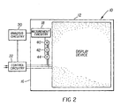
- a plurality of reference pixels could be used (see Fig. 2).
- the pixels in the display device 12 can include colored subpixels; if the operational or display characteristics of the various colored sub-pixels differ, it can be useful to include a reference pixel 40 , 42 , 44 corresponding to each color.
- reference pixels can be used as well. This will provide a wider variety of measurements and their various results can be combined to provide an overall feedback signal less subject to noise, process variation, failure, and so on. It is also possible to have reference pixels associated with specific portions of the display or to use actual display pixels as reference pixels. It is also possible to have a plurality of reference pixels and associated measurement circuits, wherein each measurement circuit measures a different performance attribute.
- the measurement and analysis circuitry can be integrated directly onto the same substrate as the display device or it can be implemented externally to the display. In general, higher performance and greater accuracy can be achieved by integrating the circuitry directly with the reference pixels but this may not be desirable for all display devices. (For example, the pixel technology and manufacturing process may inhibit the integration of measurement circuitry and logic.)
- This concept can be extended to the analysis and even the feedback control circuitry. These may also be integrated in various ways on the display device itself. System issues such as power, the implementation of control and timing logic, etc., and the effective integration of the various functions in the system will dictate the best approach.
- a properly instrumented reference pixel provides feedback in support of operational changes that accommodate changes in the pixels over time, it can also be used to modify the technique used to control the brightness of the display.
- the light output by organic LED devices depends directly on the current through the OLED. As current changes, the light output changes.
- current regulation within a solid-state electronic device is much more difficult to achieve than voltage regulation.
- a display mechanism that relies upon voltage control is preferred and will reduce design costs and increase the pixel fill factor (reducing the area needed for transistors).
- This preferred approach can be achieved through the use of a reference pixel. By measuring the impedance across a reference pixel at a given voltage, the current can be compared to the desired current. By modifying the voltage, the impedance and hence current can be modified until it meets the desired level.
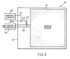
- a current measurement circuit 26 implements the generic measurement circuit 18 of Fig. 1.
- the control circuitry 24 of Fig. 1 is divided into two parts, the voltage signal 28 applied to the reference pixel (the power signal) and the data and select lines 30 (the control signals) applied to the reference pixel.
- This current measurement circuit 26 measures the current passing through the reference pixel 14 as a function of the voltage and control signals.
- the current measurement and voltage value is transferred to the analysis circuit 20 through signal 32 .
- the analysis circuit compares the voltage and current to its desired values for the pixel and adjusts the voltage signal 28 through the control circuitry 22 .
- the desired values can be obtained from a table relating desired current to pixel value.
- a behavioral model for the pixel can be utilized to provide the desired current value and consequent voltage adjustment. This same adjusted voltage is then applied to all of the pixels in the display device.
- the use of feedback from a reference pixel enables an appropriately compensated voltage driven display that operates with the benefits of current regulation.
- a higher quality current regulated imaging display device can be manufactured at the lower cost of a voltage driven device.
- a separate measurement circuit is used to compensate the voltage appropriately either with a single compromise voltage or with a separate control for each type of pixel.
- the measurement circuit in this case the current measurement circuit, could be resident on the same substrate as the reference pixel or not.
- This approach to controlling organic LED displays extends to compensation for aging properties as well. As the organic materials age, the current required to maintain a certain level of brightness increases and the impedance (for a given brightness) increases. Compensation for this effect can be achieved through an increased voltage, mediated through the measured impedance as described above. Hence, this invention can serve to ameliorate the negative effect of aging materials within an organic LED display.
- the voltage through a pixel device can be achieved.
- the first is to increase the operating voltage of the device, the second is by changing the response corresponding to each code value used to represent pixel brightness of the display pixel, and the third by modulating the length of time for which the pixel is on. Any of these techniques, or combination of techniques, will work but may be limited in their dynamic range. These techniques are limited by the operational limits of the device.
- the invention is employed in a device that includes Organic Light Emitting Diodes (OLEDs), which are composed of small molecule polymeric OLEDs, as disclosed in, but not limited to, U.S. Patent No. 4,769,292 issued September 6, 1988 to Tang et al., and U.S. Patent No. 5,061,569 issued October 29, 1991 to VanSlyke et al.
- OLEDs Organic Light Emitting Diodes
- Many combinations and variations of OLED can be used to fabricate such a device.
- OLED devices can be integrated in a micro-circuit on a conventional silicon substrate 10 and exhibit the necessary characteristics.
- OLED devices may also be integrated upon other substrates, such as glass or steel having a pattern of conductive oxide and amorphous, polycrystalline, or continuous grain silicon material deposited thereon.
- the deposited silicon materials may be single-crystal in nature or be amorphous, polycrystalline, or continuous grain.
- the integration of reference pixels, the measurement of their performance, and appropriate feedback to the control of the display device can enhance the image quality, lifetime, and power consumption of a digital image display system.
Landscapes
- Engineering & Computer Science (AREA)
- Physics & Mathematics (AREA)
- Computer Hardware Design (AREA)
- General Physics & Mathematics (AREA)
- Theoretical Computer Science (AREA)
- Control Of Indicators Other Than Cathode Ray Tubes (AREA)
- Electroluminescent Light Sources (AREA)
- Control Of El Displays (AREA)
Abstract
Description
In either case, once a determination is made that the performance of the device needs to be modified, the analysis circuitry signals the feedback and control mechanism that initiates the change.
Claims (44)
- A system for controlling a digital image display device having addressable pixels on a substrate, the pixels having performance attributes, and a control circuit for controlling the pixels of the display device, comprising:a) a reference pixel located on the substrate and connected to the control circuit, the reference pixel having the same performance attributes as the pixels in the display;b) a measurement circuit connected to the reference pixel to produce an output signal representative of the performance attributes of the reference pixel;c) an analysis circuit connected to the measurement circuit to receive the output signal, compare the performance attributes with predetermined performance attributes, and produce a feedback signal in response thereto; andd) the control circuit being adapted to receive the feedback signal and control the digital solid-state display device in response thereto.
- The system claimed in claim 1 wherein the performance attributes measured are one or more attributes selected from the list including charge stored, impedance, current, voltage, and resistivity.
- The system claimed in claim 1, further comprising a plurality of reference pixels and measurement circuits connected to the analysis circuit.
- The system claimed in claim 3 wherein the display includes different types of pixels having different performance attributes and the reference pixels include a pixel of each type.
- The system claimed in claim 4 wherein the types of pixels include pixels of different colors.
- The system claimed in claim 3 wherein the reference pixels include multiple identical pixels whose results are combined whereby the measured performance attribute is more accurately measured.
- The system claimed in claim 1 wherein the analysis circuit compares the reference pixel performance attributes to a model of pixel behavior.
- The system claimed in claim 1 wherein the analysis circuit compares the reference pixel attributes to empirical data relating to the performance of an exemplary display.
- The system claimed in claim 1 wherein the analysis device compares the reference pixel attributes to historical reference pixel attribute data.
- The system claimed in claim 1 wherein the measurement circuit is integrated on the same substrate as the reference pixel.
- The system claimed in claim 1 wherein the analysis circuit is integrated on the substrate.
- The system claimed in claim 1 wherein the feedback control circuit is integrated on the substrate.
- The system claimed in claim 1 wherein the measurement circuit measures the current in the reference pixel and the control circuit produces a voltage signal to control the current applied to the pixels of the display.
- The system claimed in claim 13 wherein the measurement circuit measures the impedance or current of a reference pixel and the control circuit modifies the operational voltage of the display to provide a constant current supply to the display pixels.
- The system claimed in claim 1 wherein the pixels are organic LEDs.
- The system claimed in claim 15 wherein the measurement circuit measures the impedance or current of a reference pixel and the circuit modifies the operational voltage of the display to provide a constant current supply to the display pixels to compensate for change in pixel impedance due to change in the OLEDs over time.
- The system claimed in claim 3, wherein each measurement circuit measures a different performance attribute.
- The system claimed in claim 1, wherein the reference pixel is also a display pixel.
- The system claimed in claim 1, wherein the control circuit controls the voltage applied to the entire display device.
- The system claimed in claim 1, wherein the control circuit controls the voltage applied to groups of pixels on the display device.
- The system claimed in claim 1, wherein the control circuit modifies the response to the code values used to represent pixel brightness.
- The system claimed in claim 1, wherein the control circuit controls the time that voltage or charge is applied to the pixels in the display device.
- A method for controlling a digital image display device having addressable pixels on a substrate, the pixels having performance attributes, and a control circuit for controlling the pixels of the display device, comprising the steps of:a) providing a reference pixel located on the substrate and connected to the control circuit, the reference pixel having the same performance attributes as the pixels in the display;b) measuring the output of the reference pixel to produce an output signal representative of the performance attributes of the reference pixel;c) analyzing the output signal by comparing the performance attributes with predetermined performance attributes, and producing a feedback signal in response thereto; andd) controlling the digital solid-state display device in response to the feedback signal.
- The method claimed in claim 23 wherein the performance attributes measured are one or more attributes selected from the list including charge stored, impedance, current, voltage, and resistivity.
- The method claimed in claim 23, further comprising the steps of providing a plurality of reference pixels and measuring the outputs thereof.
- The method claimed in claim 25 wherein the display includes different types of pixels having different performance attributes and the reference pixels include a pixel of each type.
- The method claimed in claim 26 wherein the types of pixels include pixels of different colors.
- The method claimed in claim 25 wherein the reference pixels include multiple identical pixels whose results are combined whereby the measured performance attribute is more accurately measured.
- The method claimed in claim 23 wherein the analyzing step includes comparing the reference pixel performance attributes to a model of pixel behavior.
- The method claimed in claim 23 wherein the analyzing step includes comparing the reference pixel attributes to empirical data relating to the performance of an exemplary display.
- The method claimed in claim 23 wherein the analyzing step includes comparing the reference pixel attributes to historical reference pixel attribute data.
- The method claimed in claim 23 wherein the measuring step is performed with a measuring circuit that is integrated on the same substrate as the reference pixel.
- The method claimed in claim 23 wherein the analyzing step is performed with an analysis circuit that is integrated on the substrate.
- The method claimed in claim 23 wherein the controlling step is performed by a control circuit that is integrated on the substrate.
- The method claimed in claim 23 wherein the measuring step is performed by a measurement circuit that measures the current in the reference pixel and the controlling step is performed by a control circuit that produces a voltage signal to control the current applied to the pixels of the display.
- The method claimed in claim 35 wherein the measuring step includes measuring the impedance or current of a reference pixel and the controlling step includes modifying the operational voltage of the display to provide a constant current supply to the display pixels.
- The method claimed in claim 23 wherein the pixels are organic LEDs.
- The method claimed in claim 37 wherein the measuring step includes measuring the impedance or current of a reference pixel and modifying the operational voltage of the display to provide a constant current supply to the display pixels to compensate for the change in pixel impedance due to the aging of the OLEDs.
- The method claimed in claim 25, wherein each measurement measures a different performance attribute.
- The method claimed in claim 23, wherein the reference pixel is also a display pixel.
- The method claimed in claim 23, wherein the controlling step includes controlling the voltage applied to the entire display device.
- The method claimed in claim 23, wherein the controlling step includes controlling the voltage applied to groups of pixels on the display device.
- The method claimed in claim 23, wherein the controlling step includes modifying the response to the code values used to represent pixel brightness.
- The method claimed in claim 23, wherein the controlling step includes controlling the time that voltage or charge is applied to the pixels in the display device.
Applications Claiming Priority (2)
| Application Number | Priority Date | Filing Date | Title |
|---|---|---|---|
| US57724100A | 2000-05-24 | 2000-05-24 | |
| US577241 | 2000-05-24 |
Publications (2)
| Publication Number | Publication Date |
|---|---|
| EP1158483A2 true EP1158483A2 (en) | 2001-11-28 |
| EP1158483A3 EP1158483A3 (en) | 2003-02-05 |
Family
ID=24307873
Family Applications (1)
| Application Number | Title | Priority Date | Filing Date |
|---|---|---|---|
| EP01201792A Withdrawn EP1158483A3 (en) | 2000-05-24 | 2001-05-14 | Solid-state display with reference pixel |
Country Status (3)
| Country | Link |
|---|---|
| US (1) | US7321348B2 (en) |
| EP (1) | EP1158483A3 (en) |
| JP (1) | JP2002023686A (en) |
Cited By (11)
| Publication number | Priority date | Publication date | Assignee | Title |
|---|---|---|---|---|
| EP1318499A3 (en) * | 2001-11-27 | 2003-08-27 | Pioneer Corporation | Display apparatus with active matrix type display panel |
| WO2004025615A1 (en) * | 2002-09-16 | 2004-03-25 | Koninklijke Philips Electronics N.V. | Display device |
| WO2004088626A1 (en) * | 2003-04-01 | 2004-10-14 | Koninklijke Philips Electronics N.V. | Active matrix display devices with modelling circuit located outside the display area for compensating threshold variations of the pixel drive transistor |
| FR2854252A1 (en) * | 2003-04-25 | 2004-10-29 | Thales Sa | DEVICE FOR SERVING COLORIMETRIC PHOTO PARAMETERS FOR LIGHT BOX WITH COLORED LEDS |
| EP1879169A1 (en) * | 2006-07-14 | 2008-01-16 | Barco N.V. | Aging compensation for display boards comprising light emitting elements |
| EP1879172A1 (en) * | 2006-07-14 | 2008-01-16 | Barco NV | Aging compensation for display boards comprising light emitting elements |
| US7321348B2 (en) | 2000-05-24 | 2008-01-22 | Eastman Kodak Company | OLED display with aging compensation |
| WO2008025985A1 (en) | 2006-08-31 | 2008-03-06 | Cambridge Display Technology Limited | Display drive systems |
| EP2159783A1 (en) * | 2008-09-01 | 2010-03-03 | Barco N.V. | Method and system for compensating ageing effects in light emitting diode display devices |
| CN102005181A (en) * | 2010-11-19 | 2011-04-06 | 深圳市金立翔光电科技有限公司 | Standard dot matrix light source and image point correction method of LED display screen |
| CN111986613A (en) * | 2019-05-22 | 2020-11-24 | 西安诺瓦星云科技股份有限公司 | Display correction method and device, display correction system and computer readable medium |
Families Citing this family (212)
| Publication number | Priority date | Publication date | Assignee | Title |
|---|---|---|---|---|
| EP1388767B1 (en) * | 1996-09-24 | 2006-04-26 | Seiko Epson Corporation | Projector display comprising light source units |
| JP2002304155A (en) * | 2001-01-29 | 2002-10-18 | Semiconductor Energy Lab Co Ltd | Light emitting device |
| US7569849B2 (en) | 2001-02-16 | 2009-08-04 | Ignis Innovation Inc. | Pixel driver circuit and pixel circuit having the pixel driver circuit |
| US7009590B2 (en) * | 2001-05-15 | 2006-03-07 | Sharp Kabushiki Kaisha | Display apparatus and display method |
| US7446743B2 (en) * | 2001-09-11 | 2008-11-04 | Intel Corporation | Compensating organic light emitting device displays for temperature effects |
| JP2003122305A (en) * | 2001-10-10 | 2003-04-25 | Sony Corp | Organic EL display device and control method thereof |
| US20030071821A1 (en) * | 2001-10-11 | 2003-04-17 | Sundahl Robert C. | Luminance compensation for emissive displays |
| US7253813B2 (en) | 2002-02-01 | 2007-08-07 | Seiko Epson Corporation | Electro-optical device, driving method thereof, and electronic apparatus |
| EP1355289B1 (en) * | 2002-04-15 | 2008-07-02 | Pioneer Corporation | Drive unit of self-luminous device with degradation detection function |
| JP4651922B2 (en) * | 2002-08-09 | 2011-03-16 | 株式会社半導体エネルギー研究所 | EL display device |
| JP4423848B2 (en) | 2002-10-31 | 2010-03-03 | ソニー株式会社 | Image display device and color balance adjustment method thereof |
| US7161566B2 (en) * | 2003-01-31 | 2007-01-09 | Eastman Kodak Company | OLED display with aging compensation |
| CA2419704A1 (en) | 2003-02-24 | 2004-08-24 | Ignis Innovation Inc. | Method of manufacturing a pixel with organic light-emitting diode |
| CA2443206A1 (en) | 2003-09-23 | 2005-03-23 | Ignis Innovation Inc. | Amoled display backplanes - pixel driver circuits, array architecture, and external compensation |
| US6995519B2 (en) * | 2003-11-25 | 2006-02-07 | Eastman Kodak Company | OLED display with aging compensation |
| JP4007336B2 (en) * | 2004-04-12 | 2007-11-14 | セイコーエプソン株式会社 | Pixel circuit driving method, pixel circuit, electro-optical device, and electronic apparatus |
| US7295192B2 (en) * | 2004-05-04 | 2007-11-13 | Au Optronics Corporation | Compensating color shift of electro-luminescent displays |
| JP4850436B2 (en) * | 2004-05-21 | 2012-01-11 | 株式会社半導体エネルギー研究所 | Display device and electronic apparatus using the same |
| TWI287212B (en) * | 2004-06-02 | 2007-09-21 | Chi Mei Optoelectronics Corp | Driving circuit, compensation circuit of pixel structures of active organic electro-luminescence device and signal compensating method thereof |
| TWI238374B (en) * | 2004-06-17 | 2005-08-21 | Au Optronics Corp | Organic light emitting diode display, display luminance compensating device thereof, and compensating method thereof |
| US20060044227A1 (en) * | 2004-06-18 | 2006-03-02 | Eastman Kodak Company | Selecting adjustment for OLED drive voltage |
| CA2472671A1 (en) * | 2004-06-29 | 2005-12-29 | Ignis Innovation Inc. | Voltage-programming scheme for current-driven amoled displays |
| US7540978B2 (en) * | 2004-08-05 | 2009-06-02 | Novaled Ag | Use of an organic matrix material for producing an organic semiconductor material, organic semiconductor material and electronic component |
| DE102004045871B4 (en) * | 2004-09-20 | 2006-11-23 | Novaled Gmbh | Method and circuit arrangement for aging compensation of organic light emitting diodes |
| JP4510735B2 (en) * | 2004-09-22 | 2010-07-28 | 統寶光電股▲ふん▼有限公司 | Design method, panel and its electronic device |
| EP1648042B1 (en) * | 2004-10-07 | 2007-05-02 | Novaled AG | A method for doping a semiconductor material with cesium |
| US7400345B2 (en) * | 2004-10-22 | 2008-07-15 | Eastman Kodak Company | OLED display with aspect ratio compensation |
| US20060119592A1 (en) * | 2004-12-06 | 2006-06-08 | Jian Wang | Electronic device and method of using the same |
| CA2490858A1 (en) | 2004-12-07 | 2006-06-07 | Ignis Innovation Inc. | Driving method for compensated voltage-programming of amoled displays |
| DE102004060201A1 (en) * | 2004-12-14 | 2006-06-29 | Schreiner Group Gmbh & Co. Kg | Method and control electronics to compensate for the aging-related loss of brightness of an Elektroluminezenzelements |
| US7619597B2 (en) | 2004-12-15 | 2009-11-17 | Ignis Innovation Inc. | Method and system for programming, calibrating and driving a light emitting device display |
| US9280933B2 (en) | 2004-12-15 | 2016-03-08 | Ignis Innovation Inc. | System and methods for extraction of threshold and mobility parameters in AMOLED displays |
| US9171500B2 (en) | 2011-05-20 | 2015-10-27 | Ignis Innovation Inc. | System and methods for extraction of parasitic parameters in AMOLED displays |
| US8599191B2 (en) | 2011-05-20 | 2013-12-03 | Ignis Innovation Inc. | System and methods for extraction of threshold and mobility parameters in AMOLED displays |
| US8576217B2 (en) | 2011-05-20 | 2013-11-05 | Ignis Innovation Inc. | System and methods for extraction of threshold and mobility parameters in AMOLED displays |
| US10013907B2 (en) | 2004-12-15 | 2018-07-03 | Ignis Innovation Inc. | Method and system for programming, calibrating and/or compensating, and driving an LED display |
| US10012678B2 (en) | 2004-12-15 | 2018-07-03 | Ignis Innovation Inc. | Method and system for programming, calibrating and/or compensating, and driving an LED display |
| US9275579B2 (en) | 2004-12-15 | 2016-03-01 | Ignis Innovation Inc. | System and methods for extraction of threshold and mobility parameters in AMOLED displays |
| US9799246B2 (en) | 2011-05-20 | 2017-10-24 | Ignis Innovation Inc. | System and methods for extraction of threshold and mobility parameters in AMOLED displays |
| US20140111567A1 (en) | 2005-04-12 | 2014-04-24 | Ignis Innovation Inc. | System and method for compensation of non-uniformities in light emitting device displays |
| JP4934963B2 (en) * | 2005-01-21 | 2012-05-23 | ソニー株式会社 | Burn-in phenomenon correction method, self-luminous device, burn-in phenomenon correction apparatus, and program |
| CA2495726A1 (en) | 2005-01-28 | 2006-07-28 | Ignis Innovation Inc. | Locally referenced voltage programmed pixel for amoled displays |
| CA2496642A1 (en) | 2005-02-10 | 2006-08-10 | Ignis Innovation Inc. | Fast settling time driving method for organic light-emitting diode (oled) displays based on current programming |
| TWI409768B (en) * | 2005-03-02 | 2013-09-21 | Innolux Corp | Active matrix display devices and methods of driving the same |
| JP4419872B2 (en) * | 2005-03-08 | 2010-02-24 | セイコーエプソン株式会社 | Display device and display module |
| US20080158115A1 (en) * | 2005-04-04 | 2008-07-03 | Koninklijke Philips Electronics, N.V. | Led Display System |
| JP2006301220A (en) * | 2005-04-20 | 2006-11-02 | Hitachi Displays Ltd | Display device and driving method thereof |
| DE502005009415D1 (en) * | 2005-05-27 | 2010-05-27 | Novaled Ag | Transparent organic light emitting diode |
| EP2045843B1 (en) * | 2005-06-01 | 2012-08-01 | Novaled AG | Light-emitting component with an electrode assembly |
| US7852298B2 (en) | 2005-06-08 | 2010-12-14 | Ignis Innovation Inc. | Method and system for driving a light emitting device display |
| DE502005003742D1 (en) * | 2005-06-14 | 2008-05-29 | Novaled Ag | A method of operating an organic light emitting device and organic light emitting device |
| EP1739765A1 (en) * | 2005-07-01 | 2007-01-03 | Novaled AG | Organic light-emitting diode and stack of organic light emitting diodes |
| US8692740B2 (en) * | 2005-07-04 | 2014-04-08 | Semiconductor Energy Laboratory Co., Ltd. | Display device and driving method thereof |
| CA2510855A1 (en) * | 2005-07-06 | 2007-01-06 | Ignis Innovation Inc. | Fast driving method for amoled displays |
| KR101446340B1 (en) * | 2005-08-11 | 2014-10-01 | 엘지디스플레이 주식회사 | Electro-Luminescence Display Apparatus |
| DE102005042704A1 (en) * | 2005-09-01 | 2007-03-08 | Ingenieurbüro Kienhöfer GmbH | A method of operating a display device having a plurality of weary pixels and display device |
| CA2518276A1 (en) | 2005-09-13 | 2007-03-13 | Ignis Innovation Inc. | Compensation technique for luminance degradation in electro-luminance devices |
| EP1932137B1 (en) * | 2005-09-29 | 2016-07-13 | OLEDWorks GmbH | A method of compensating an aging process of an illumination device |
| KR101315088B1 (en) | 2005-10-20 | 2013-10-07 | 코닌클리케 필립스 엔.브이. | Lighting device |
| US7479660B2 (en) | 2005-10-21 | 2009-01-20 | Perkinelmer Elcos Gmbh | Multichip on-board LED illumination device |
| DE102005061204A1 (en) * | 2005-12-21 | 2007-07-05 | Perkinelmer Elcos Gmbh | Lighting device, lighting control device and lighting system |
| US7371616B2 (en) | 2006-01-05 | 2008-05-13 | Fairchild Semiconductor Corporation | Clipless and wireless semiconductor die package and method for making the same |
| US9269322B2 (en) | 2006-01-09 | 2016-02-23 | Ignis Innovation Inc. | Method and system for driving an active matrix display circuit |
| CA2570898C (en) | 2006-01-09 | 2008-08-05 | Ignis Innovation Inc. | Method and system for driving an active matrix display circuit |
| US9489891B2 (en) | 2006-01-09 | 2016-11-08 | Ignis Innovation Inc. | Method and system for driving an active matrix display circuit |
| US7924249B2 (en) * | 2006-02-10 | 2011-04-12 | Ignis Innovation Inc. | Method and system for light emitting device displays |
| JP5130634B2 (en) * | 2006-03-08 | 2013-01-30 | ソニー株式会社 | Self-luminous display device, electronic device, burn-in correction device, and program |
| JP4577244B2 (en) * | 2006-03-15 | 2010-11-10 | セイコーエプソン株式会社 | LIGHT EMITTING DEVICE, ITS DRIVE METHOD, AND ELECTRONIC DEVICE |
| US8232931B2 (en) * | 2006-04-10 | 2012-07-31 | Emagin Corporation | Auto-calibrating gamma correction circuit for AMOLED pixel display driver |
| US20080048951A1 (en) * | 2006-04-13 | 2008-02-28 | Naugler Walter E Jr | Method and apparatus for managing and uniformly maintaining pixel circuitry in a flat panel display |
| EP2008264B1 (en) | 2006-04-19 | 2016-11-16 | Ignis Innovation Inc. | Stable driving scheme for active matrix displays |
| US20080002070A1 (en) * | 2006-06-29 | 2008-01-03 | Eastman Kodak Company | Driving oled display with improved uniformity |
| US20080042938A1 (en) * | 2006-08-15 | 2008-02-21 | Cok Ronald S | Driving method for el displays with improved uniformity |
| CA2556961A1 (en) | 2006-08-15 | 2008-02-15 | Ignis Innovation Inc. | Oled compensation technique based on oled capacitance |
| TWI348677B (en) * | 2006-09-12 | 2011-09-11 | Ind Tech Res Inst | System for increasing circuit reliability and method thereof |
| KR100872352B1 (en) * | 2006-11-28 | 2008-12-09 | 한국과학기술원 | Data driving circuit and organic light emitting display device including the same |
| JP5317419B2 (en) * | 2007-03-07 | 2013-10-16 | 株式会社ジャパンディスプレイ | Organic EL display device |
| US8077123B2 (en) * | 2007-03-20 | 2011-12-13 | Leadis Technology, Inc. | Emission control in aged active matrix OLED display using voltage ratio or current ratio with temperature compensation |
| US20080231557A1 (en) * | 2007-03-20 | 2008-09-25 | Leadis Technology, Inc. | Emission control in aged active matrix oled display using voltage ratio or current ratio |
| TWI453711B (en) * | 2007-03-21 | 2014-09-21 | Semiconductor Energy Lab | Display device |
| JP2009025735A (en) * | 2007-07-23 | 2009-02-05 | Hitachi Displays Ltd | Image display device |
| JP4893537B2 (en) * | 2007-08-27 | 2012-03-07 | パナソニック電工株式会社 | Light emitting module and manufacturing method thereof |
| JP5142791B2 (en) * | 2008-04-01 | 2013-02-13 | 株式会社ジャパンディスプレイイースト | Display device |
| KR20100134125A (en) | 2008-04-18 | 2010-12-22 | 이그니스 이노베이션 인크. | System and driving method for light emitting device display |
| TW201006256A (en) * | 2008-07-16 | 2010-02-01 | Acer Inc | Automatic color adjustment method and automatic color adjustment device |
| CA2637343A1 (en) | 2008-07-29 | 2010-01-29 | Ignis Innovation Inc. | Improving the display source driver |
| US9370075B2 (en) | 2008-12-09 | 2016-06-14 | Ignis Innovation Inc. | System and method for fast compensation programming of pixels in a display |
| US8130904B2 (en) * | 2009-01-29 | 2012-03-06 | The Invention Science Fund I, Llc | Diagnostic delivery service |
| US8249218B2 (en) * | 2009-01-29 | 2012-08-21 | The Invention Science Fund I, Llc | Diagnostic delivery service |
| US20100201275A1 (en) | 2009-02-06 | 2010-08-12 | Cok Ronald S | Light sensing in display device |
| US8350495B2 (en) | 2009-06-05 | 2013-01-08 | Light-Based Technologies Incorporated | Device driver providing compensation for aging |
| CA2669367A1 (en) | 2009-06-16 | 2010-12-16 | Ignis Innovation Inc | Compensation technique for color shift in displays |
| US10319307B2 (en) | 2009-06-16 | 2019-06-11 | Ignis Innovation Inc. | Display system with compensation techniques and/or shared level resources |
| US9384698B2 (en) | 2009-11-30 | 2016-07-05 | Ignis Innovation Inc. | System and methods for aging compensation in AMOLED displays |
| CA2688870A1 (en) | 2009-11-30 | 2011-05-30 | Ignis Innovation Inc. | Methode and techniques for improving display uniformity |
| US9311859B2 (en) | 2009-11-30 | 2016-04-12 | Ignis Innovation Inc. | Resetting cycle for aging compensation in AMOLED displays |
| JP5310372B2 (en) * | 2009-08-12 | 2013-10-09 | ソニー株式会社 | Display device, luminance degradation correction method, and electronic device |
| US8339386B2 (en) * | 2009-09-29 | 2012-12-25 | Global Oled Technology Llc | Electroluminescent device aging compensation with reference subpixels |
| EP2316332A1 (en) | 2009-10-30 | 2011-05-04 | General Electric Company | Sensor for measuring amount of substance in blood and method of making the sensor |
| US8633873B2 (en) | 2009-11-12 | 2014-01-21 | Ignis Innovation Inc. | Stable fast programming scheme for displays |
| US10996258B2 (en) | 2009-11-30 | 2021-05-04 | Ignis Innovation Inc. | Defect detection and correction of pixel circuits for AMOLED displays |
| CA2686174A1 (en) * | 2009-12-01 | 2011-06-01 | Ignis Innovation Inc | High reslution pixel architecture |
| US8803417B2 (en) | 2009-12-01 | 2014-08-12 | Ignis Innovation Inc. | High resolution pixel architecture |
| CA2687631A1 (en) * | 2009-12-06 | 2011-06-06 | Ignis Innovation Inc | Low power driving scheme for display applications |
| US10176736B2 (en) | 2010-02-04 | 2019-01-08 | Ignis Innovation Inc. | System and methods for extracting correlation curves for an organic light emitting device |
| US9881532B2 (en) | 2010-02-04 | 2018-01-30 | Ignis Innovation Inc. | System and method for extracting correlation curves for an organic light emitting device |
| US10089921B2 (en) | 2010-02-04 | 2018-10-02 | Ignis Innovation Inc. | System and methods for extracting correlation curves for an organic light emitting device |
| US10163401B2 (en) | 2010-02-04 | 2018-12-25 | Ignis Innovation Inc. | System and methods for extracting correlation curves for an organic light emitting device |
| US20140313111A1 (en) | 2010-02-04 | 2014-10-23 | Ignis Innovation Inc. | System and methods for extracting correlation curves for an organic light emitting device |
| CA2692097A1 (en) | 2010-02-04 | 2011-08-04 | Ignis Innovation Inc. | Extracting correlation curves for light emitting device |
| CA2696778A1 (en) | 2010-03-17 | 2011-09-17 | Ignis Innovation Inc. | Lifetime, uniformity, parameter extraction methods |
| KR101065405B1 (en) * | 2010-04-14 | 2011-09-16 | 삼성모바일디스플레이주식회사 | Display device and driving method |
| US8711099B2 (en) | 2010-05-10 | 2014-04-29 | Blackberry Limited | Handheld electronic communication device having sliding display |
| JP2011243894A (en) * | 2010-05-21 | 2011-12-01 | Sanken Electric Co Ltd | Organic el lighting device |
| TWI423214B (en) * | 2010-07-06 | 2014-01-11 | 財團法人工業技術研究院 | Pixel driving circuit and pixel driving method |
| WO2012033746A2 (en) | 2010-09-07 | 2012-03-15 | Venmill Industries, Inc. | Illuminable wall socket plates and systems and methods thereof |
| US8668347B2 (en) | 2010-09-16 | 2014-03-11 | Cordell Eldred Ebeling | Receptacle cover |
| US8907991B2 (en) | 2010-12-02 | 2014-12-09 | Ignis Innovation Inc. | System and methods for thermal compensation in AMOLED displays |
| US8723890B2 (en) | 2010-12-23 | 2014-05-13 | Blackberry Limited | Handheld electronic device having sliding display and position configurable camera |
| US8532721B2 (en) | 2010-12-23 | 2013-09-10 | Blackberry Limited | Portable electronic device having sliding display providing event notification |
| US8514179B2 (en) | 2010-12-23 | 2013-08-20 | Research In Motion Limited | Handheld electronic communication device having an age compensating display |
| US8773451B2 (en) | 2011-05-03 | 2014-07-08 | Apple Inc. | Color correction method and apparatus for displays |
| US20140368491A1 (en) | 2013-03-08 | 2014-12-18 | Ignis Innovation Inc. | Pixel circuits for amoled displays |
| US9351368B2 (en) | 2013-03-08 | 2016-05-24 | Ignis Innovation Inc. | Pixel circuits for AMOLED displays |
| US9606607B2 (en) | 2011-05-17 | 2017-03-28 | Ignis Innovation Inc. | Systems and methods for display systems with dynamic power control |
| US9886899B2 (en) | 2011-05-17 | 2018-02-06 | Ignis Innovation Inc. | Pixel Circuits for AMOLED displays |
| CN105869575B (en) | 2011-05-17 | 2018-09-21 | 伊格尼斯创新公司 | The method for operating display |
| US9530349B2 (en) | 2011-05-20 | 2016-12-27 | Ignis Innovations Inc. | Charged-based compensation and parameter extraction in AMOLED displays |
| US9466240B2 (en) | 2011-05-26 | 2016-10-11 | Ignis Innovation Inc. | Adaptive feedback system for compensating for aging pixel areas with enhanced estimation speed |
| JP2014517940A (en) | 2011-05-27 | 2014-07-24 | イグニス・イノベイション・インコーポレーテッド | System and method for aging compensation in AMOLED displays |
| EP2715711A4 (en) | 2011-05-28 | 2014-12-24 | Ignis Innovation Inc | System and method for fast compensation programming of pixels in a display |
| US12142880B2 (en) | 2011-08-01 | 2024-11-12 | Snaprays, Llc | Active cover plates |
| US12021335B2 (en) | 2017-02-17 | 2024-06-25 | Snaprays, Llc | Active cover plates |
| US11664631B2 (en) | 2011-08-01 | 2023-05-30 | Snaprays, Llc | Environment sensing active units |
| US9070775B2 (en) | 2011-08-03 | 2015-06-30 | Ignis Innovations Inc. | Thin film transistor |
| US8901579B2 (en) | 2011-08-03 | 2014-12-02 | Ignis Innovation Inc. | Organic light emitting diode and method of manufacturing |
| US10089924B2 (en) | 2011-11-29 | 2018-10-02 | Ignis Innovation Inc. | Structural and low-frequency non-uniformity compensation |
| US9324268B2 (en) | 2013-03-15 | 2016-04-26 | Ignis Innovation Inc. | Amoled displays with multiple readout circuits |
| US9385169B2 (en) | 2011-11-29 | 2016-07-05 | Ignis Innovation Inc. | Multi-functional active matrix organic light-emitting diode display |
| KR101334100B1 (en) * | 2011-12-30 | 2013-11-29 | (주)실리콘화일 | Apparatus for bright compensation of oled panel |
| US8937632B2 (en) | 2012-02-03 | 2015-01-20 | Ignis Innovation Inc. | Driving system for active-matrix displays |
| US9190456B2 (en) | 2012-04-25 | 2015-11-17 | Ignis Innovation Inc. | High resolution display panel with emissive organic layers emitting light of different colors |
| US9747834B2 (en) | 2012-05-11 | 2017-08-29 | Ignis Innovation Inc. | Pixel circuits including feedback capacitors and reset capacitors, and display systems therefore |
| US8922544B2 (en) | 2012-05-23 | 2014-12-30 | Ignis Innovation Inc. | Display systems with compensation for line propagation delay |
| US9526141B2 (en) * | 2012-11-21 | 2016-12-20 | Lighthouse Technologies Limited | Automatic color adjustment on LED screens |
| US9786223B2 (en) | 2012-12-11 | 2017-10-10 | Ignis Innovation Inc. | Pixel circuits for AMOLED displays |
| US9336717B2 (en) | 2012-12-11 | 2016-05-10 | Ignis Innovation Inc. | Pixel circuits for AMOLED displays |
| US9830857B2 (en) | 2013-01-14 | 2017-11-28 | Ignis Innovation Inc. | Cleaning common unwanted signals from pixel measurements in emissive displays |
| CN104981862B (en) | 2013-01-14 | 2018-07-06 | 伊格尼斯创新公司 | Driving scheme for emissive displays providing compensation for drive transistor variations |
| CA2894717A1 (en) | 2015-06-19 | 2016-12-19 | Ignis Innovation Inc. | Optoelectronic device characterization in array with shared sense line |
| US9721505B2 (en) | 2013-03-08 | 2017-08-01 | Ignis Innovation Inc. | Pixel circuits for AMOLED displays |
| EP2779147B1 (en) | 2013-03-14 | 2016-03-02 | Ignis Innovation Inc. | Re-interpolation with edge detection for extracting an aging pattern for AMOLED displays |
| US9952698B2 (en) | 2013-03-15 | 2018-04-24 | Ignis Innovation Inc. | Dynamic adjustment of touch resolutions on an AMOLED display |
| DE112014002086T5 (en) | 2013-04-22 | 2016-01-14 | Ignis Innovation Inc. | Test system for OLED display screens |
| KR102150011B1 (en) * | 2013-06-10 | 2020-09-01 | 삼성디스플레이 주식회사 | Organic light emitting display device and method of manufacturing having the same |
| KR102025118B1 (en) | 2013-06-18 | 2019-09-26 | 삼성디스플레이 주식회사 | Pixel and organic light emitting display including the same |
| CN107452314B (en) | 2013-08-12 | 2021-08-24 | 伊格尼斯创新公司 | Method and apparatus for compensating image data for an image to be displayed by a display |
| CN107967897B (en) * | 2013-12-05 | 2021-09-03 | 伊格尼斯创新公司 | Pixel circuit and method for extracting circuit parameters and providing in-pixel compensation |
| US9761170B2 (en) | 2013-12-06 | 2017-09-12 | Ignis Innovation Inc. | Correction for localized phenomena in an image array |
| US9741282B2 (en) | 2013-12-06 | 2017-08-22 | Ignis Innovation Inc. | OLED display system and method |
| US9502653B2 (en) | 2013-12-25 | 2016-11-22 | Ignis Innovation Inc. | Electrode contacts |
| US10997901B2 (en) | 2014-02-28 | 2021-05-04 | Ignis Innovation Inc. | Display system |
| US10176752B2 (en) | 2014-03-24 | 2019-01-08 | Ignis Innovation Inc. | Integrated gate driver |
| DE102015206281A1 (en) | 2014-04-08 | 2015-10-08 | Ignis Innovation Inc. | Display system with shared level resources for portable devices |
| CA2872563A1 (en) | 2014-11-28 | 2016-05-28 | Ignis Innovation Inc. | High pixel density array architecture |
| CA2873476A1 (en) | 2014-12-08 | 2016-06-08 | Ignis Innovation Inc. | Smart-pixel display architecture |
| CA2879462A1 (en) | 2015-01-23 | 2016-07-23 | Ignis Innovation Inc. | Compensation for color variation in emissive devices |
| CA2886862A1 (en) | 2015-04-01 | 2016-10-01 | Ignis Innovation Inc. | Adjusting display brightness for avoiding overheating and/or accelerated aging |
| US10235936B2 (en) | 2015-04-10 | 2019-03-19 | Apple Inc. | Luminance uniformity correction for display panels |
| US10134334B2 (en) | 2015-04-10 | 2018-11-20 | Apple Inc. | Luminance uniformity correction for display panels |
| CA2889870A1 (en) | 2015-05-04 | 2016-11-04 | Ignis Innovation Inc. | Optical feedback system |
| CA2892714A1 (en) | 2015-05-27 | 2016-11-27 | Ignis Innovation Inc | Memory bandwidth reduction in compensation system |
| US10657895B2 (en) | 2015-07-24 | 2020-05-19 | Ignis Innovation Inc. | Pixels and reference circuits and timing techniques |
| US10373554B2 (en) | 2015-07-24 | 2019-08-06 | Ignis Innovation Inc. | Pixels and reference circuits and timing techniques |
| CA2898282A1 (en) | 2015-07-24 | 2017-01-24 | Ignis Innovation Inc. | Hybrid calibration of current sources for current biased voltage progra mmed (cbvp) displays |
| CA2900170A1 (en) | 2015-08-07 | 2017-02-07 | Gholamreza Chaji | Calibration of pixel based on improved reference values |
| CA2908285A1 (en) | 2015-10-14 | 2017-04-14 | Ignis Innovation Inc. | Driver with multiple color pixel structure |
| CA2909813A1 (en) | 2015-10-26 | 2017-04-26 | Ignis Innovation Inc | High ppi pattern orientation |
| CN105280139B (en) * | 2015-11-11 | 2018-05-01 | 深圳市华星光电技术有限公司 | AMOLED luminance compensation methods and AMOLED drive systems |
| CN105280140B (en) * | 2015-11-24 | 2018-02-16 | 深圳市华星光电技术有限公司 | Sensing circuit and corresponding OLED display devices |
| CN106128358B (en) * | 2016-08-31 | 2018-12-18 | 京东方科技集团股份有限公司 | The driving method of display panel, the drive system of display panel and its display device |
| US10453432B2 (en) | 2016-09-24 | 2019-10-22 | Apple Inc. | Display adjustment |
| DE102017222059A1 (en) | 2016-12-06 | 2018-06-07 | Ignis Innovation Inc. | Pixel circuits for reducing hysteresis |
| CN106531081B (en) | 2017-01-23 | 2019-06-07 | 武汉华星光电技术有限公司 | A kind of display module driving device and method |
| US10475417B2 (en) * | 2017-03-29 | 2019-11-12 | Intel Corporation | History-aware selective pixel shifting |
| US10522084B2 (en) * | 2017-05-04 | 2019-12-31 | Apple Inc. | Adaptive pixel voltage compensation for display panels |
| US10714018B2 (en) | 2017-05-17 | 2020-07-14 | Ignis Innovation Inc. | System and method for loading image correction data for displays |
| CN107039004B (en) * | 2017-06-08 | 2019-04-30 | 深圳市华星光电半导体显示技术有限公司 | The aging compensation approach of AMOLED display panel |
| US11025899B2 (en) | 2017-08-11 | 2021-06-01 | Ignis Innovation Inc. | Optical correction systems and methods for correcting non-uniformity of emissive display devices |
| WO2019058442A1 (en) * | 2017-09-20 | 2019-03-28 | シャープ株式会社 | Display device and method for driving display device |
| CN108281110B (en) * | 2018-01-12 | 2020-03-10 | 深圳市华星光电半导体显示技术有限公司 | Brightness compensation method and related product |
| US10971078B2 (en) | 2018-02-12 | 2021-04-06 | Ignis Innovation Inc. | Pixel measurement through data line |
| WO2019187068A1 (en) * | 2018-03-30 | 2019-10-03 | シャープ株式会社 | Display device |
| CN108665855A (en) * | 2018-07-18 | 2018-10-16 | 深圳市华星光电技术有限公司 | The drive system and AMOLED display panels of AMOLED display panels |
| CN110875009B (en) | 2018-08-30 | 2021-01-22 | 京东方科技集团股份有限公司 | Display panel and driving method thereof |
| US10997914B1 (en) | 2018-09-07 | 2021-05-04 | Apple Inc. | Systems and methods for compensating pixel voltages |
| CN109545140B (en) * | 2018-12-13 | 2020-11-10 | 昆山国显光电有限公司 | Pixel compensation circuit, method and display device |
| CN109599060B (en) * | 2019-01-11 | 2020-12-18 | 京东方科技集团股份有限公司 | Pixel compensation method, pixel compensation system and display device |
| US10785845B1 (en) | 2019-05-24 | 2020-09-22 | Apple Inc. | Electronic devices with backlit displays |
| KR102644541B1 (en) | 2019-07-18 | 2024-03-07 | 삼성전자주식회사 | Method of sensing threshold voltage in display panel and display driver integrated circuit performing the same |
| JP2021071680A (en) * | 2019-11-01 | 2021-05-06 | セイコーエプソン株式会社 | Display device, head-mounted display device, and display method |
| CN110992894B (en) * | 2019-12-10 | 2022-04-05 | 武汉天马微电子有限公司 | Display compensation circuit, method, display panel and display device |
| US11143693B2 (en) | 2020-02-20 | 2021-10-12 | Facebook Technologies, Llc | Systems having dedicated light emitting diodes for performance characterization |
| KR102773250B1 (en) | 2020-05-22 | 2025-02-28 | 삼성디스플레이 주식회사 | Display device |
| US11961473B2 (en) * | 2020-11-27 | 2024-04-16 | Sharp Kabushiki Kaisha | Display device |
| CN112908254A (en) * | 2021-01-28 | 2021-06-04 | 上海天马有机发光显示技术有限公司 | Display panel, brightness compensation method of display panel and display device |
| US11955072B2 (en) | 2021-06-10 | 2024-04-09 | Emagin Corporation | OLED-based display having pixel compensation and method |
| US11862095B2 (en) | 2021-06-17 | 2024-01-02 | Emagin Corporation | OLED-based display having pixel compensation and method |
| US12106712B2 (en) * | 2021-10-05 | 2024-10-01 | Wuhan Tianma Micro-Electronics Co., Ltd. | Display device |
| TWI759255B (en) * | 2021-10-29 | 2022-03-21 | 大陸商昆山瑞創芯電子有限公司 | Organic light-emitting diode display device and operating method thereof |
| US12211435B2 (en) | 2022-11-18 | 2025-01-28 | Apple Inc. | Display panel transistor gate-signal compensation systems and methods |
| JP2025032927A (en) * | 2023-08-28 | 2025-03-12 | Tianma Japan株式会社 | Display device |
Family Cites Families (41)
| Publication number | Priority date | Publication date | Assignee | Title |
|---|---|---|---|---|
| US5019807A (en) * | 1984-07-25 | 1991-05-28 | Staplevision, Inc. | Display screen |
| US4769292A (en) | 1987-03-02 | 1988-09-06 | Eastman Kodak Company | Electroluminescent device with modified thin film luminescent zone |
| US4751659A (en) | 1987-08-26 | 1988-06-14 | Xerox Corporation | Defect compensation for discrete image bars |
| US5281690A (en) * | 1989-03-30 | 1994-01-25 | Brewer Science, Inc. | Base-soluble polyimide release layers for use in microlithographic processing |
| GB2237400B (en) * | 1989-10-27 | 1994-04-20 | Eev Ltd | Control of liquid crystal display visual properties |
| US5061569A (en) | 1990-07-26 | 1991-10-29 | Eastman Kodak Company | Electroluminescent device with organic electroluminescent medium |
| JPH04269790A (en) * | 1991-02-26 | 1992-09-25 | Matsushita Electric Ind Co Ltd | Information display device |
| GB9115401D0 (en) | 1991-07-17 | 1991-09-04 | Philips Electronic Associated | Matrix display device and its method of operation |
| US5216504A (en) | 1991-09-25 | 1993-06-01 | Display Laboratories, Inc. | Automatic precision video monitor alignment system |
| US5281960A (en) | 1991-11-19 | 1994-01-25 | Silhouette Technology, Inc. | Helmet mounted display |
| US5521639A (en) | 1992-04-30 | 1996-05-28 | Sony Corporation | Solid-state imaging apparatus including a reference pixel in the optically-black region |
| US5592215A (en) | 1993-02-03 | 1997-01-07 | Rohm Co., Ltd. | Stereoscopic picture system and stereoscopic display panel therefor |
| US5499040A (en) | 1994-06-27 | 1996-03-12 | Radius Inc. | Method and apparatus for display calibration and control |
| US6329758B1 (en) | 1994-12-20 | 2001-12-11 | Unisplay S.A. | LED matrix display with intensity and color matching of the pixels |
| JP3392967B2 (en) | 1994-12-27 | 2003-03-31 | ペンタックス株式会社 | Still video camera |
| US6157356A (en) * | 1996-04-12 | 2000-12-05 | International Business Machines Company | Digitally driven gray scale operation of active matrix OLED displays |
| US5754294A (en) | 1996-05-03 | 1998-05-19 | Virginia Semiconductor, Inc. | Optical micrometer for measuring thickness of transparent wafers |
| JPH1062734A (en) | 1996-08-22 | 1998-03-06 | Sony Corp | Defective pixel correction method and defective pixel correction device for liquid crystal display device |
| EP0923067B1 (en) * | 1997-03-12 | 2004-08-04 | Seiko Epson Corporation | Pixel circuit, display device and electronic equipment having current-driven light-emitting device |
| JP3767877B2 (en) | 1997-09-29 | 2006-04-19 | 三菱化学株式会社 | Active matrix light emitting diode pixel structure and method thereof |
| US5910792A (en) | 1997-11-12 | 1999-06-08 | Candescent Technologies, Corp. | Method and apparatus for brightness control in a field emission display |
| US6423900B1 (en) * | 1998-02-17 | 2002-07-23 | Technical Systems Corp. | Active cover plate for an electrical outlet |
| US6504565B1 (en) | 1998-09-21 | 2003-01-07 | Canon Kabushiki Kaisha | Light-emitting device, exposure device, and image forming apparatus |
| EP1042775A2 (en) * | 1998-09-22 | 2000-10-11 | Fed Corporation | Inorganic-based color conversion matrix element for organic color display devices and method of fabrication |
| JP3961729B2 (en) | 1999-03-03 | 2007-08-22 | 株式会社デンソー | All-focus imaging device |
| EP1079361A1 (en) * | 1999-08-20 | 2001-02-28 | Harness System Technologies Research, Ltd. | Driver for electroluminescent elements |
| WO2001020591A1 (en) * | 1999-09-11 | 2001-03-22 | Koninklijke Philips Electronics N.V. | Active matrix electroluminescent display device |
| JP2001110565A (en) * | 1999-10-04 | 2001-04-20 | Auto Network Gijutsu Kenkyusho:Kk | Display element driving device |
| US6414661B1 (en) | 2000-02-22 | 2002-07-02 | Sarnoff Corporation | Method and apparatus for calibrating display devices and automatically compensating for loss in their efficiency over time |
| EP1158483A3 (en) | 2000-05-24 | 2003-02-05 | Eastman Kodak Company | Solid-state display with reference pixel |
| US6774578B2 (en) | 2000-09-19 | 2004-08-10 | Semiconductor Energy Laboratory Co., Ltd. | Self light emitting device and method of driving thereof |
| JP3865209B2 (en) * | 2000-09-19 | 2007-01-10 | 株式会社半導体エネルギー研究所 | Self-luminous device, electronic equipment |
| JP2002278514A (en) | 2001-03-19 | 2002-09-27 | Sharp Corp | Electro-optical device |
| US6963321B2 (en) | 2001-05-09 | 2005-11-08 | Clare Micronix Integrated Systems, Inc. | Method of providing pulse amplitude modulation for OLED display drivers |
| US20020171611A1 (en) | 2001-05-15 | 2002-11-21 | Eastman Kodak Company | Active matrix organic light emitting diode flat-panel display |
| US6456016B1 (en) | 2001-07-30 | 2002-09-24 | Intel Corporation | Compensating organic light emitting device displays |
| US7274363B2 (en) | 2001-12-28 | 2007-09-25 | Pioneer Corporation | Panel display driving device and driving method |
| GB2389951A (en) * | 2002-06-18 | 2003-12-24 | Cambridge Display Tech Ltd | Display driver circuits for active matrix OLED displays |
| US20040150594A1 (en) | 2002-07-25 | 2004-08-05 | Semiconductor Energy Laboratory Co., Ltd. | Display device and drive method therefor |
| CN1682267A (en) * | 2002-09-16 | 2005-10-12 | 皇家飞利浦电子股份有限公司 | Display device |
| US20040222954A1 (en) * | 2003-04-07 | 2004-11-11 | Lueder Ernst H. | Methods and apparatus for a display |
-
2001
- 2001-05-14 EP EP01201792A patent/EP1158483A3/en not_active Withdrawn
- 2001-05-23 JP JP2001153532A patent/JP2002023686A/en active Pending
-
2003
- 2003-11-13 US US10/712,337 patent/US7321348B2/en not_active Expired - Lifetime
Cited By (20)
| Publication number | Priority date | Publication date | Assignee | Title |
|---|---|---|---|---|
| US7321348B2 (en) | 2000-05-24 | 2008-01-22 | Eastman Kodak Company | OLED display with aging compensation |
| US7233302B2 (en) | 2001-11-27 | 2007-06-19 | Pioneer Corporation | Display apparatus with active matrix type display panel |
| EP1318499A3 (en) * | 2001-11-27 | 2003-08-27 | Pioneer Corporation | Display apparatus with active matrix type display panel |
| WO2004025615A1 (en) * | 2002-09-16 | 2004-03-25 | Koninklijke Philips Electronics N.V. | Display device |
| WO2004088626A1 (en) * | 2003-04-01 | 2004-10-14 | Koninklijke Philips Electronics N.V. | Active matrix display devices with modelling circuit located outside the display area for compensating threshold variations of the pixel drive transistor |
| FR2854252A1 (en) * | 2003-04-25 | 2004-10-29 | Thales Sa | DEVICE FOR SERVING COLORIMETRIC PHOTO PARAMETERS FOR LIGHT BOX WITH COLORED LEDS |
| EP1879172A1 (en) * | 2006-07-14 | 2008-01-16 | Barco NV | Aging compensation for display boards comprising light emitting elements |
| EP1879169A1 (en) * | 2006-07-14 | 2008-01-16 | Barco N.V. | Aging compensation for display boards comprising light emitting elements |
| US8106858B2 (en) | 2006-07-14 | 2012-01-31 | Barco N.V. | Aging compensation for display boards comprising light emitting elements |
| CN101105913B (en) * | 2006-07-14 | 2012-05-23 | 巴科股份有限公司 | Aging compensation for display boards comprising light emitting elements |
| CN101523471B (en) * | 2006-08-31 | 2012-06-27 | 剑桥显示技术有限公司 | Display drive system |
| WO2008025985A1 (en) | 2006-08-31 | 2008-03-06 | Cambridge Display Technology Limited | Display drive systems |
| KR101509823B1 (en) * | 2006-08-31 | 2015-04-06 | 캠브리지 디스플레이 테크놀로지 리미티드 | OLED display driver, OLED display pixel driver circuit, method of calibrating OLED display device for burn-in of OLED display pixel, device and computer program code |
| US8427512B2 (en) | 2006-08-31 | 2013-04-23 | Cambridge Display Technology Limited | Display drive systems |
| WO2010023270A1 (en) * | 2008-09-01 | 2010-03-04 | Barco N.V. | Method and system for compensating ageing effects in light emitting diode display devices |
| EP2159783A1 (en) * | 2008-09-01 | 2010-03-03 | Barco N.V. | Method and system for compensating ageing effects in light emitting diode display devices |
| US9058769B2 (en) | 2008-09-01 | 2015-06-16 | Barco N.V. | Method and system for compensating ageing effects in light emitting diode display devices |
| CN102005181B (en) * | 2010-11-19 | 2012-09-05 | 深圳市立翔慧科光电科技有限公司 | Standard dot matrix light source and image point correction method of LED display screen |
| CN102005181A (en) * | 2010-11-19 | 2011-04-06 | 深圳市金立翔光电科技有限公司 | Standard dot matrix light source and image point correction method of LED display screen |
| CN111986613A (en) * | 2019-05-22 | 2020-11-24 | 西安诺瓦星云科技股份有限公司 | Display correction method and device, display correction system and computer readable medium |
Also Published As
| Publication number | Publication date |
|---|---|
| JP2002023686A (en) | 2002-01-23 |
| US7321348B2 (en) | 2008-01-22 |
| US20040070558A1 (en) | 2004-04-15 |
| EP1158483A3 (en) | 2003-02-05 |
Similar Documents
| Publication | Publication Date | Title |
|---|---|---|
| US8860708B2 (en) | Active matrix display drive control systems | |
| US11341934B2 (en) | Display device and image display system having the same | |
| JP2002023686A (en) | Solid display including reference pixel | |
| EP1667102B1 (en) | Backlight driving device, backlight driving method, and liquid crystal display device | |
| KR100475526B1 (en) | Drive circuit for active matrix light emitting device | |
| CN100452137C (en) | Drivers for OLED Passive Matrix Displays | |
| CN108428721A (en) | A kind of display device and control method | |
| KR102496782B1 (en) | Voltage conversion circuit and organic lighting emitting device having the saeme | |
| EP1260959A2 (en) | Active matrix organic light emitting diode flat-panel display | |
| KR20090063207A (en) | Compensation method for organic light emitting diode luminance deterioration | |
| KR20190049977A (en) | Method for setting black data of disply device and disply device employing the same | |
| KR20250072566A (en) | Image data corrector and display device having the same | |
| EP3726519A1 (en) | Display drive module, display device, and voltage adjustment method | |
| KR20220090189A (en) | Organic light emitting display apparatus | |
| KR20080010796A (en) | OLED display and driving method thereof | |
| CN101661706A (en) | Display driving circuit and display device using the same | |
| KR101142281B1 (en) | Organic electro luminescent display and driving method of the same | |
| US20080106554A1 (en) | Organic light emitting diode pixel circuit and brightness control method thereof | |
| US20080117196A1 (en) | Display device and driving method thereof | |
| EP1747682A1 (en) | Colour display device | |
| KR20060014253A (en) | Gamma reference voltage providing device and liquid crystal display device | |
| JP2004271759A (en) | Driving semiconductor circuit group for current driven display device and current driven display device using the semiconductor circuit group | |
| KR101986109B1 (en) | Organic light emitting display device and method for driving the same | |
| JP5153331B2 (en) | Active matrix image display device and control method thereof | |
| KR20160035906A (en) | Orgainc emitting diode display device and method for driving the same |
Legal Events
| Date | Code | Title | Description |
|---|---|---|---|
| PUAI | Public reference made under article 153(3) epc to a published international application that has entered the european phase |
Free format text: ORIGINAL CODE: 0009012 |
|
| AK | Designated contracting states |
Kind code of ref document: A2 Designated state(s): AT BE CH CY DE DK ES FI FR GB GR IE IT LI LU MC NL PT SE TR |
|
| AX | Request for extension of the european patent |
Free format text: AL;LT;LV;MK;RO;SI |
|
| PUAL | Search report despatched |
Free format text: ORIGINAL CODE: 0009013 |
|
| AK | Designated contracting states |
Designated state(s): AT BE CH CY DE DK ES FI FR GB GR IE IT LI LU MC NL PT SE TR |
|
| AX | Request for extension of the european patent |
Extension state: AL LT LV MK RO SI |
|
| 17P | Request for examination filed |
Effective date: 20030716 |
|
| 17Q | First examination report despatched |
Effective date: 20030908 |
|
| AKX | Designation fees paid |
Designated state(s): DE FR GB |
|
| STAA | Information on the status of an ep patent application or granted ep patent |
Free format text: STATUS: THE APPLICATION IS DEEMED TO BE WITHDRAWN |
|
| 18D | Application deemed to be withdrawn |
Effective date: 20040119 |