EP1158316A1 - Beugungsgitter mit hohem Aspektverhältnis sowie Verwendungen dieses Beugungsgitters - Google Patents
Beugungsgitter mit hohem Aspektverhältnis sowie Verwendungen dieses Beugungsgitters Download PDFInfo
- Publication number
- EP1158316A1 EP1158316A1 EP01110569A EP01110569A EP1158316A1 EP 1158316 A1 EP1158316 A1 EP 1158316A1 EP 01110569 A EP01110569 A EP 01110569A EP 01110569 A EP01110569 A EP 01110569A EP 1158316 A1 EP1158316 A1 EP 1158316A1
- Authority
- EP
- European Patent Office
- Prior art keywords
- diffraction grating
- web
- grating according
- diffraction
- reflection
- Prior art date
- Legal status (The legal status is an assumption and is not a legal conclusion. Google has not performed a legal analysis and makes no representation as to the accuracy of the status listed.)
- Granted
Links
- 239000011248 coating agent Substances 0.000 claims abstract description 12
- 238000000576 coating method Methods 0.000 claims abstract description 12
- VYPSYNLAJGMNEJ-UHFFFAOYSA-N silicon dioxide Inorganic materials O=[Si]=O VYPSYNLAJGMNEJ-UHFFFAOYSA-N 0.000 claims abstract description 9
- XAGFODPZIPBFFR-UHFFFAOYSA-N aluminium Chemical compound [Al] XAGFODPZIPBFFR-UHFFFAOYSA-N 0.000 claims abstract description 7
- 229910052782 aluminium Inorganic materials 0.000 claims abstract description 7
- 239000010453 quartz Substances 0.000 claims abstract description 4
- 238000002310 reflectometry Methods 0.000 claims description 6
- 229910052710 silicon Inorganic materials 0.000 claims description 4
- 239000010703 silicon Substances 0.000 claims description 4
- 229910018072 Al 2 O 3 Inorganic materials 0.000 claims description 3
- 229910017768 LaF 3 Inorganic materials 0.000 claims description 3
- 238000005259 measurement Methods 0.000 claims description 3
- 229910001635 magnesium fluoride Inorganic materials 0.000 abstract 2
- 229910002319 LaF3 Inorganic materials 0.000 abstract 1
- PNEYBMLMFCGWSK-UHFFFAOYSA-N aluminium oxide Inorganic materials [O-2].[O-2].[O-2].[Al+3].[Al+3] PNEYBMLMFCGWSK-UHFFFAOYSA-N 0.000 abstract 1
- 229910052593 corundum Inorganic materials 0.000 abstract 1
- BYMUNNMMXKDFEZ-UHFFFAOYSA-K trifluorolanthanum Chemical compound F[La](F)F BYMUNNMMXKDFEZ-UHFFFAOYSA-K 0.000 abstract 1
- 229910001845 yogo sapphire Inorganic materials 0.000 abstract 1
- 230000010287 polarization Effects 0.000 description 24
- 238000004519 manufacturing process Methods 0.000 description 17
- 229920002120 photoresistant polymer Polymers 0.000 description 12
- 238000010521 absorption reaction Methods 0.000 description 6
- 238000005530 etching Methods 0.000 description 5
- 239000000463 material Substances 0.000 description 5
- 230000003287 optical effect Effects 0.000 description 5
- 238000010884 ion-beam technique Methods 0.000 description 4
- 238000001020 plasma etching Methods 0.000 description 4
- 230000008901 benefit Effects 0.000 description 3
- 238000000034 method Methods 0.000 description 3
- 239000012876 carrier material Substances 0.000 description 2
- 238000003486 chemical etching Methods 0.000 description 2
- 239000013078 crystal Substances 0.000 description 2
- 238000013461 design Methods 0.000 description 2
- 238000011161 development Methods 0.000 description 2
- 230000003993 interaction Effects 0.000 description 2
- 239000007787 solid Substances 0.000 description 2
- ISQINHMJILFLAQ-UHFFFAOYSA-N argon hydrofluoride Chemical compound F.[Ar] ISQINHMJILFLAQ-UHFFFAOYSA-N 0.000 description 1
- 238000004364 calculation method Methods 0.000 description 1
- 239000002178 crystalline material Substances 0.000 description 1
- 229910021419 crystalline silicon Inorganic materials 0.000 description 1
- 238000005520 cutting process Methods 0.000 description 1
- 230000001419 dependent effect Effects 0.000 description 1
- 238000010586 diagram Methods 0.000 description 1
- 238000005516 engineering process Methods 0.000 description 1
- 238000001459 lithography Methods 0.000 description 1
- 238000003754 machining Methods 0.000 description 1
- 238000005457 optimization Methods 0.000 description 1
- 238000012545 processing Methods 0.000 description 1
- 239000004065 semiconductor Substances 0.000 description 1
Images


Classifications
-
- G—PHYSICS
- G02—OPTICS
- G02B—OPTICAL ELEMENTS, SYSTEMS OR APPARATUS
- G02B5/00—Optical elements other than lenses
- G02B5/18—Diffraction gratings
- G02B5/1838—Diffraction gratings for use with ultraviolet radiation or X-rays
-
- G—PHYSICS
- G02—OPTICS
- G02B—OPTICAL ELEMENTS, SYSTEMS OR APPARATUS
- G02B5/00—Optical elements other than lenses
- G02B5/18—Diffraction gratings
- G02B5/1814—Diffraction gratings structurally combined with one or more further optical elements, e.g. lenses, mirrors, prisms or other diffraction gratings
-
- G—PHYSICS
- G02—OPTICS
- G02B—OPTICAL ELEMENTS, SYSTEMS OR APPARATUS
- G02B5/00—Optical elements other than lenses
- G02B5/18—Diffraction gratings
- G02B5/1861—Reflection gratings characterised by their structure, e.g. step profile, contours of substrate or grooves, pitch variations, materials
-
- G—PHYSICS
- G03—PHOTOGRAPHY; CINEMATOGRAPHY; ANALOGOUS TECHNIQUES USING WAVES OTHER THAN OPTICAL WAVES; ELECTROGRAPHY; HOLOGRAPHY
- G03H—HOLOGRAPHIC PROCESSES OR APPARATUS
- G03H1/00—Holographic processes or apparatus using light, infrared or ultraviolet waves for obtaining holograms or for obtaining an image from them; Details peculiar thereto
- G03H1/02—Details of features involved during the holographic process; Replication of holograms without interference recording
- G03H1/024—Hologram nature or properties
- G03H1/0244—Surface relief holograms
Definitions
- the invention relates to a diffraction grating with a Many parallel, periodically successive Diffraction structures arranged on a carrier are and each one of a base of the Include carrier from extending web. Furthermore concerns the invention uses such a diffraction grating.
- Known diffraction gratings of this type are particularly suitable for the direction of polarization that is perpendicular to the longitudinal direction the web is standing (TM polarization), a relatively poor reflection efficiency, i.e. a relatively poor diffraction efficiency in the diffraction order used. This also fluctuates strongly with the angle of incidence or the light wavelength.
- the Fluctuation range of reflection efficiency in a relative narrow range around the angle of incidence or the light wavelength i.e. the distance between a minimum and a
- the maximum value within this range is Range of tens of percent.
- the optical arrangement in which the known diffraction grating has been used has been the default leave the resulting reflection efficiency to chance: e.g. can for the TM polarization direction for these specifications there is just a minimum of reflection efficiency.
- the reflection efficiency is high Diffraction gratings for a given light wavelength and a predetermined angle of incidence is required, e.g. a reflection efficiency in the range of the maximum value of the Reflection efficiencies for this polarization direction, that for this grid type in the area around the given one Direction of incidence or light wavelength can be achieved, this cannot be tolerated.
- the web has a substantially rectangular cross section has, the perpendicular to the central plane of the web and the width of the web measured parallel to the base area less than 100 nm, preferably between 20 nm and 60 nm, more preferably in the range of 50 nm.
- the webs of the diffraction grating according to the invention are also referred to as "narrow" Called bridges.
- a bill that shows the interaction the light rays with TM polarization with the ridges includes, it can be shown that with these web widths surprisingly a much better reflection efficiency of the diffraction grating also for TM polarization results. This also fluctuates depending on the Direction of incidence and the wavelength of the incident Beams of light not like with known diffraction gratings wider ridges strong.
- Grid with these narrow bars can therefore be used for the respective application in which Angle of incidence and light wavelength are specified by Adjust the choice of the appropriate lattice constant without the mentioned fluctuations in reflection efficiency for the TM polarization must be accepted or a special optimization of the diffraction grating on the specified parameter pair "light wavelength” and "direction of incidence” must be carried out.
- the height of the web above the base can be more than 200 nm, preferably between 200 nm and 600 nm.
- the polarization interaction was also surprising including account that the The reflection efficiencies depend on the web heights. Above The reflection efficiencies approached a web height of 200 nm very quickly to an optimal value which only increases when the bridge height is increased repeated periodically. Again from manufacturing technology There are reasons for a given Lowest web height belonging to reflection efficiency.
- the central plane of the web can be perpendicular to the base stand.
- Such a diffraction grating can be relatively easy to manufacture because the preferred direction of Bridge processing perpendicular to the base of the beam stands.
- the central plane of the web with the base include an angle other than 90 °.
- the base of the carrier can also be achieved that the web flank facing the incident light beam in the range of a blaze angle for the respective application of the diffraction grating. An additional increase the reflection efficiency is the result.
- the diffraction grating preferably consists of quartz glass or Silicon.
- Such materials can be reactive Ion beam etching (RIBE) or by reactive ion etching (RIE) edit and therefore offer themselves for holographic Production of the diffraction structures according to the invention on.
- RIBE reactive Ion beam etching
- RIE reactive ion etching
- crystalline material such as e.g. Silicon can also be added to the crystal surface crystallographic orientation of the crystal in such a way align that there is a preferred direction during machining, e.g. B. by anisotropic chemical etching with KOH, results. This preferred direction can, for. B. at the Take advantage of the production of inclined webs according to claim 4.
- the diffraction grating can be made of doped quartz consist. Because of its advantageous expansion behavior such a material is suitable for use.
- the layer sequence can be selected so that an additional, increasing the reflection efficiency of the diffraction grating Coating can be dispensed with.
- the layer system can comprise a plurality of successive layers of Al 2 O 3 (high refractive index) and MgF 2 (low refractive index) or of LaF 3 (high refractive index) and MgF 2 (low refractive index).
- Such an alternating layer system is well suited for producing a highly reflective layer for ultraviolet light wavelengths.
- the diffraction grating has a reflectivity increasing Coating on, can in turn be dispensed with, to design the carrier as a dielectric layer system, while still achieving a high reflectivity.
- the carrier For optical applications that require a subsequent coating allow with a reflective layer results such a cheaper manufacture of the diffraction grating.
- the coating is preferably an aluminum coating. Such a coating is relative inexpensive and has a high achievable reflectivity on.
- Another object of the present invention is es, uses for the diffraction grating according to the invention specify in which the illustrated benefits of the diffraction grating be used well. This task is solved by the preferred uses listed below:
- a preferred use of the diffraction grating is that as a reflection grating in a Littrow configuration.
- Such an optical arrangement is given often lattice constant due to manufacturing and fixed Light wavelength also the direction of incidence of the light rays fixed. So there is no room for variation here for the design of the optical arrangement, so that the Advantage of not critical of the parameters "direction of incidence” or "light wavelength” dependent reflection efficiency of the diffraction grating for the TM polarization fully for Wear comes.
- the diffraction grating is preferably in the third order the light wavelength used. Especially with small ones Light wavelengths, e.g. B. in the UV range as a result, reduced production requirements of the diffraction grating, as a larger one in the third order Distance of the diffraction structures than in the first order the diffraction condition is met.
- An advantageous area of use for the diffraction grating is the diffraction of UV light with a wavelength, which is less than 250 nm.
- Such UV light sources are particularly useful in projection lithography Manufacture of semiconductor structures in chip manufacture in use.
- the wavelength of such a projection light source Select narrowband and efficiently.
- Another preferred use of the diffraction grating is a phase grating for interferometric length measurement. This use is also high Grid efficiency required by using the Diffraction grating according to the invention is guaranteed.
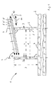
- Figure 1 shows a section of a total with the Reference number 1 provided with reflection diffraction grating a carrier 2 on which a variety of periodically arranged webs 3 are formed, of which in Figure 1 shows two webs 3 as examples in cross section are.
- the carrier 2 and the webs 3 consist of quartz glass.
- the webs 3 each have a width w of 20 nm, measured in each case on the upper end face of the web 3 perpendicular to whose center plane 7, which in turn perpendicular to the plane of the drawing of Figure 1 runs.
- the height D of the webs 3 above the base area 4 is 250 nm.
- the webs 3 have a rectangular cross section, i.e. the flanks 5, 6 of a web 3 close with the base 4 a substantially right angle.
- the central plane 7 of each web 3 is on the Base area 4 vertical.
- the thickness of the carrier 2 is compared to the height D of the webs 3 is very large, e.g. in the range of several millimeters, which is why the carrier 2 in Figure 1 is interrupted is shown.
- a diffraction structure of the reflection diffraction grating 1 each comprises a web 3 and an adjacent one Space a to the next web 3.
- the width d of such a diffraction structure is therefore the sum of the web width w and the space a between two webs 3.
- the width d depends on in which optical application the reflection diffraction grating 1 is used. In the case shown in FIG. 1, which is described below is the width d 297 nm.
- the reflection diffraction grating works in the Littrow configuration 1 as follows:
- the reflection diffraction grating 1 arranged so that the central planes 7th the webs 3 with the incident light rays 8, 9 Littrow angle theta of 77 °, which is indicated for the Width d and a light wavelength of 193.35 nm results in third order include.
- the specified The wavelength of light is that of an argon fluoride excimer laser.
- the incident light beams 8, 9 can both perpendicular to the direction of extension of the webs 3 (TM polarization, Light wave 8 ') and parallel to the direction of extension the bars must be polarized (TE polarization, Light waves 8 '', 8 '' '), as shown schematically in Figure 1 is shown.
- the diffraction condition i.e. the condition of constructive interference from third parties Order fulfilled.
- the reflection diffraction grating 1 acts So for the incident light rays 8, 9 with the Wavelength 193.35 nm as a mirror that the incident Light rays 8, 9 in third diffraction order in themselves reflected back.
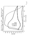
- TM polarization Reflection efficiency of> 80% in a web width range between about 8 and about 15 nm. In a web width range the reflection efficiency lies between approx. 5 and approx. 22 nm for TM polarization over 60%. In these described areas of high reflection efficiency is the Absorption of the radiated light waves always lower than 30%, in the case of TE polarization even less than 10%.
- a lattice blank is made 13 made of quartz glass coated with a photoresist mask 12, exposed holographically and then developed.
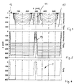
- figure 4 is the time course of the cross section of this Structure in the course of the development of the photoresist mask 12 shown.
- the top curve of Figure 4 represents the undeveloped photoresist mask 12, the plane thereof Surface parallel to that of the lattice blank 13 is.
- the individual curves shown in figure 4 show the current height of the photoresist in the course of this photoresist removal to successive ones Times.
- the photoresist bars 14 have to each other according to the specification by exposure the distance that is needed for the diffraction structures desired distance of 295.8 nm results.
- FIG. 5 shows the course over time of the cross section of the lattice blank 13 with the photoresist bars 14 during this process. Both the photoresist bars 14 and the lattice blank 13 are removed in layers with a vertical preferred direction until an etching depth of approximately 550 nm, measured from the original surface of the photoresist mask 12, is reached in the lattice blank 13.
- the bottom curve of FIG. 5 represents this state.
- the reflection diffraction grating 101 from FIG. 7 has one Aluminum layer 115 on. This has a thickness of approx. 20 nm.
- the reflection diffraction grating 101 with the aluminum layer 115 became a coating technique chosen with a preferred direction so that namely the surfaces of the carrier 102 and the web 103, but not the flanks 105, 106 of the web 103 are coated. Alternatively, the flanks can also be used of a web is coated reflectively in an analogous manner become.
- the aluminum layer 115 has a reflectivity from almost 100%.
- FIG. 8 shows the reflection diffraction grating 201 produce with webs 203, the flanks 205, 206 of which are not stand at right angles on the base 204, but enclose with it an angle ⁇ other than 90 °, that the web 203 stronger at its base is as at its top.
- To increase efficiency of the reflection diffraction grating 201 can tilt of flanks 205, 206 e.g. to be such that one Blaze angle for the appropriate use of the reflection diffraction grating 201 corresponds.
- the reflection diffraction grating shown in FIG. 9 301 are selected by choosing the preferred direction that described in connection with Figures 4 to 6 Manufacturing process the middle planes 307 of the webs 303 inclined to the base 304 of the carrier 302.
- the incident light wave 308 falls 308 almost perpendicular to the central planes 307 of the webs 303 on the grid 301.
- reflection diffraction gratings 1 to 301 is not on the Littrow configuration described limited.
- Other applications e.g. as a blaze grid (Angle of incidence not equal to angle of reflection) are conceivable here also the inclination of the middle planes 7 to 307 or edges 5 to 305; 6 to 306 chosen accordingly becomes.
- a grating with the diffraction structures described above can also be used as a phase grating in interferometric Length measurement can be used.
- anisotropic materials such as silicon or doped quartz or a dielectric layer system can also be used as the carrier material.
- the dielectric layer system is, for example, an alternating layering of Al 2 O 3 (high refractive index) and MgF 2 (low refractive index) or LaF 3 (high refractive index) and MgF 2 (low refractive index), for example using 40 double layers of these two materials.
- the layer thicknesses of the individual layers of the dielectric layer system are chosen so that the reflectivity of the reflection diffraction grating is optimized for the wavelength used.
- RIBE reactive ion beam etching
- RIE reactive ion etching
- IBE ion beam etching
- anisotropic chemical etching e.g. with KOH, preferably for anisotropic materials such as crystalline silicon.
Landscapes
- Physics & Mathematics (AREA)
- General Physics & Mathematics (AREA)
- Optics & Photonics (AREA)
- Health & Medical Sciences (AREA)
- Toxicology (AREA)
- Diffracting Gratings Or Hologram Optical Elements (AREA)
Abstract
Description
- Figur 1:
- einen Schnitt durch einen Ausschnitt eines Reflexions-Beugungsgitters, wobei die Schnittebene senkrecht zur Mittelebene von als Stege ausgeformten Beugungsstrukturen des Reflexions-Beugungsgitters verläuft;
- Figuren 2 und 3:
- zwei Diagramme der Abhängigkeit der Beugungseffizienz bzw. der Absorption eines Reflexions-Beugungsgitters nach Figur 1 von der Stegbreite;
- Figuren 4 bis 6:
- Momentaufnahmen bei der Herstellung eines Reflexions-Beugungsgitters nach Figur 1;
- Figuren 7 bis 9:
- zur Figur 1 ähnliche Darstellungen alternativer Ausführungsformen eines Reflexionsbeugungsgitters, wobei jeweils nur ein Steg gezeigt ist.
Claims (15)
- Beugungsgitter mit einer Vielzahl paralleler, periodisch aufeinanderfolgender Beugungsstrukturen, die auf einem Träger angeordnet sind und jeweils einen sich von einer Grundfläche des Trägers aus erstreckenden Steg umfassen,
dadurch gekennzeichnet, daß
der Steg (3; 103; 203; 303) einen im wesentlichen rechteckigen Querschnitt aufweist, wobei die senkrecht zur Mittelebene (7; 307) des Stegs (3; 103; 203; 303) und parallel zur Grundfläche (4; 104; 204; 304) gemessene Breite w des Stegs (3; 103; 203; 303) weniger als 100 nm, bevorzugt zwischen 20 nm und 60 nm, stärker bevorzugt im Bereich von 50 nm beträgt. - Beugungsgitter nach Anspruch 1, dadurch gekennzeichnet, daß die Höhe D des Stegs (3; 103; 203; 303) über der Grundfläche (4; 104; 204; 304) mehr als 200 nm, bevorzugt zwischen 200 nm und 600 nm, beträgt.
- Beugungsgitter nach Anspruch 1 oder 2, dadurch gekennzeichnet, daß die Mittelebene (7) des Stegs (3) senkrecht auf der Grundfläche (4) steht.
- Beugungsgitter nach Anspruch 1 oder 2, dadurch gekennzeichnet, daß die Mittelebene (307) des Stegs (303) mit der Grundfläche (304) einen von 90° verschiedenen Winkel einschließt.
- Beugungsgitter nach einem der vorhergehenden Ansprüche, dadurch gekennzeichnet, daß es aus Quarzglas oder Silizium besteht.
- Beugungsgitter nach einem der Ansprüche 1 bis 4,
dadurch gekennzeichnet, daß es aus dotiertem Quarz besteht. - Beugungsgitter nach einem der Ansprüche 1 bis 4,
dadurch gekennzeichnet, daß es ein dielektrisches Schichtsystem umfaßt. - Beugungsgitter nach Anspruch 7, dadurch gekennzeichnet, daß das Schichtsystem eine Mehrzahl von aufeinanderfolgenden Schichten aus Al2O3 und MgF2 umfaßt.
- Beugungsgitter nach Anspruch 7, dadurch gekennzeichnet, daß das Schichtsystem eine Mehrzahl von aufeinanderfolgenden Schichten aus LaF3 und MgF2 umfaßt.
- Beugungsgitter nach einem der Ansprüche 1 bis 6,
dadurch gekennzeichnet, daß es eine die Reflektivität steigernde Beschichtung (115) aufweist. - Beugungsgitter nach Anspruch 10, daduch gekennzeichnet,
daß die Beschichtung (115) eine Aluminium-Beschichtung ist. - Verwendung eines Beugungsgitters nach einem der vorhergehenden Ansprüche als Reflexionsgitter in einer Littrow-Konfiguration.
- Verwendung eines Beugungsgitters nach einem der Ansprüche 1 bis 11 in höherer, vorzugsweise dritter Ordnung der einfallenden Lichtwellenlänge.
- Verwendung eines Beugungsgitters nach einem der Ansprüche 1 bis 11 zur Beugung von UV-Licht (8, 9; 308) mit einer Wellenlänge, die geringer ist als 250 nm.
- Verwendung eines Beugungsgitters nach einem der Ansprüche 1 bis 11 als Phasengitter bei der interferometrischen Längenmessung.
Applications Claiming Priority (2)
| Application Number | Priority Date | Filing Date | Title |
|---|---|---|---|
| DE10025694 | 2000-05-24 | ||
| DE10025694A DE10025694C2 (de) | 2000-05-24 | 2000-05-24 | Verwendung eines Beugungsgitters |
Publications (2)
| Publication Number | Publication Date |
|---|---|
| EP1158316A1 true EP1158316A1 (de) | 2001-11-28 |
| EP1158316B1 EP1158316B1 (de) | 2003-07-23 |
Family
ID=7643380
Family Applications (1)
| Application Number | Title | Priority Date | Filing Date |
|---|---|---|---|
| EP01110569A Expired - Lifetime EP1158316B1 (de) | 2000-05-24 | 2001-04-30 | Verwendung eines Beugungsgitters mit hohem Aspektverhältnis |
Country Status (5)
| Country | Link |
|---|---|
| US (1) | US6600602B2 (de) |
| EP (1) | EP1158316B1 (de) |
| JP (1) | JP2002006126A (de) |
| DE (2) | DE10025694C2 (de) |
| TW (1) | TWI244560B (de) |
Cited By (2)
| Publication number | Priority date | Publication date | Assignee | Title |
|---|---|---|---|---|
| EP1316821A3 (de) * | 2001-11-29 | 2005-04-06 | Carl Zeiss Laser Optics GmbH | Optische Anordnung, Littrow-Gitter zur Verwendung in einer optischen Anordnung sowie Verwendung eines Littrow-Gitters |
| CN112313548A (zh) * | 2018-08-29 | 2021-02-02 | 株式会社日立高新技术 | 凹面衍射光栅以及其制造方法、和光学装置 |
Families Citing this family (11)
| Publication number | Priority date | Publication date | Assignee | Title |
|---|---|---|---|---|
| US6747799B2 (en) * | 2001-11-12 | 2004-06-08 | Pts Corporation | High-efficiency low-polarization-dependent-loss lamellar diffraction-grating profile and production process |
| DE10327963A1 (de) * | 2003-06-19 | 2005-01-05 | Carl Zeiss Jena Gmbh | Polarisationsstrahlteiler |
| TWI223103B (en) * | 2003-10-23 | 2004-11-01 | Ind Tech Res Inst | Wire grid polarizer with double metal layers |
| CN100397045C (zh) * | 2004-01-26 | 2008-06-25 | 三丰株式会社 | 标尺的制造方法和光电式编码器 |
| US7109472B2 (en) * | 2004-03-26 | 2006-09-19 | Mitutoyo Corporation | Scale for reflective photoelectric encoder and reflective photoelectric encoder |
| DE102004042748B4 (de) * | 2004-09-03 | 2007-06-06 | Trumpf Laser- Und Systemtechnik Gmbh | Konzentrisches oder spiralförmiges Beugungsgitter für einen Laserresonator |
| TW200817733A (en) * | 2006-10-14 | 2008-04-16 | Ind Tech Res Inst | Anti-radiation structure |
| US8116002B2 (en) * | 2007-08-27 | 2012-02-14 | Lumella Inc. | Grating device with adjusting layer |
| WO2010030268A1 (en) * | 2008-09-09 | 2010-03-18 | John Hoose | Grating device with adjusting layer |
| DE102010017425A1 (de) | 2010-06-17 | 2011-12-22 | Karlsruher Institut für Technologie | Geneigte Phasengitterstrukturen |
| JP6066634B2 (ja) * | 2011-10-06 | 2017-01-25 | キヤノン株式会社 | エシェル型回折格子の製造方法およびエキシマレーザの製造方法 |
Citations (7)
| Publication number | Priority date | Publication date | Assignee | Title |
|---|---|---|---|---|
| US4506949A (en) * | 1983-05-27 | 1985-03-26 | Rca Corporation | Diffractive color separation filter |
| US4714308A (en) * | 1984-02-29 | 1987-12-22 | Canon Kabushiki Kaisha | Ultraviolet reflecting mirror |
| US4915463A (en) * | 1988-10-18 | 1990-04-10 | The United States Of America As Represented By The Department Of Energy | Multilayer diffraction grating |
| US5116461A (en) * | 1991-04-22 | 1992-05-26 | Motorola, Inc. | Method for fabricating an angled diffraction grating |
| DE4421407C1 (de) * | 1994-06-18 | 1995-06-01 | Kurz Leonhard Fa | Flächenelement mit einer räumlichen, bereichsweise beschichteten Mikrostruktur sowie Verwendung eines solchen Flächenelements |
| US5629804A (en) * | 1993-01-18 | 1997-05-13 | Canon Kabushiki Kaisha | Diffraction grating |
| EP1003078A2 (de) * | 1998-11-17 | 2000-05-24 | Corning Incorporated | Verfahren zur Vervielfältigung eines Nanomusters |
Family Cites Families (9)
| Publication number | Priority date | Publication date | Assignee | Title |
|---|---|---|---|---|
| US3945825A (en) * | 1974-05-22 | 1976-03-23 | Rca Corporation | Method for producing width-modulated surface relief patterns |
| US4360586A (en) * | 1979-05-29 | 1982-11-23 | Massachusetts Institute Of Technology | Spatial period division exposing |
| IT1213280B (it) * | 1984-04-30 | 1989-12-14 | Enea | Interferometro ottico con elemento deviatore di tipo dispersivo |
| DD263362A1 (de) * | 1987-07-29 | 1988-12-28 | Zeiss Jena Veb Carl | Geblaztes holografisches reflexionsbeugungsgitter |
| US4830463A (en) | 1988-02-08 | 1989-05-16 | American Telephone And Telegraph Company, At&T Bell Laboratories | Article comprising silica-based glass containing aluminum and phorphorus |
| US4830643A (en) * | 1988-07-13 | 1989-05-16 | W. L. Gore & Associates, Inc. | Expanded polytetrafluoroethylene tubular container |
| JPH06201909A (ja) | 1992-12-28 | 1994-07-22 | Canon Inc | 回折格子の製造方法 |
| DE4303162A1 (de) * | 1993-02-04 | 1994-08-11 | Zeiss Carl Fa | Photoelektrisches Längen- bzw. Winkelmeßsystem |
| ATE210832T1 (de) * | 1995-04-13 | 2001-12-15 | Heidenhain Gmbh Dr Johannes | Ma stab und verfahren zur herstellung eines ma stabes sowie positionsmesseinrichtung |
-
2000
- 2000-05-24 DE DE10025694A patent/DE10025694C2/de not_active Expired - Fee Related
-
2001
- 2001-04-30 EP EP01110569A patent/EP1158316B1/de not_active Expired - Lifetime
- 2001-04-30 DE DE50100398T patent/DE50100398D1/de not_active Expired - Fee Related
- 2001-05-23 US US09/863,745 patent/US6600602B2/en not_active Expired - Fee Related
- 2001-05-24 JP JP2001155236A patent/JP2002006126A/ja active Pending
- 2001-05-31 TW TW090110863A patent/TWI244560B/zh not_active IP Right Cessation
Patent Citations (7)
| Publication number | Priority date | Publication date | Assignee | Title |
|---|---|---|---|---|
| US4506949A (en) * | 1983-05-27 | 1985-03-26 | Rca Corporation | Diffractive color separation filter |
| US4714308A (en) * | 1984-02-29 | 1987-12-22 | Canon Kabushiki Kaisha | Ultraviolet reflecting mirror |
| US4915463A (en) * | 1988-10-18 | 1990-04-10 | The United States Of America As Represented By The Department Of Energy | Multilayer diffraction grating |
| US5116461A (en) * | 1991-04-22 | 1992-05-26 | Motorola, Inc. | Method for fabricating an angled diffraction grating |
| US5629804A (en) * | 1993-01-18 | 1997-05-13 | Canon Kabushiki Kaisha | Diffraction grating |
| DE4421407C1 (de) * | 1994-06-18 | 1995-06-01 | Kurz Leonhard Fa | Flächenelement mit einer räumlichen, bereichsweise beschichteten Mikrostruktur sowie Verwendung eines solchen Flächenelements |
| EP1003078A2 (de) * | 1998-11-17 | 2000-05-24 | Corning Incorporated | Verfahren zur Vervielfältigung eines Nanomusters |
Non-Patent Citations (3)
| Title |
|---|
| BRUNDRETT D L ET AL: "POLARIZING MIRROR/ABSORBER FOR VISIBLE WAVELENGTHS BASED ON A SILICON SUBWAVELENGTH GRATING: DESIGN AND FABRICATION", APPLIED OPTICS, OPTICAL SOCIETY OF AMERICA,WASHINGTON, US, vol. 37, no. 13, 1 May 1998 (1998-05-01), pages 2534 - 2541, XP000754633, ISSN: 0003-6935 * |
| FISUN A I: "MONOFREQUENCY EXCITATION OF OPEN RESONATOR WITH INCLINED COMB GRATING", INTERNATIONAL JOURNAL OF INFRARED AND MILLIMETER WAVES, PLENUM PUBLISHING, NEW YORK, US, vol. 18, no. 7, 1 July 1997 (1997-07-01), pages 1431 - 1443, XP000694577, ISSN: 0195-9271 * |
| WENYONG DENG ET AL: "FABRICATION AND PROPERTIES OF VISIBLE-LIGHT SUBWAVELENGTH AMORPHOUSSILICON TRANSMISSION GRATINGS", JOURNAL OF VACUUM SCIENCE AND TECHNOLOGY: PART B, AMERICAN INSTITUTE OF PHYSICS. NEW YORK, US, vol. 13, no. 6, 1 November 1995 (1995-11-01), pages 2879 - 2882, XP000558362, ISSN: 0734-211X * |
Cited By (3)
| Publication number | Priority date | Publication date | Assignee | Title |
|---|---|---|---|---|
| EP1316821A3 (de) * | 2001-11-29 | 2005-04-06 | Carl Zeiss Laser Optics GmbH | Optische Anordnung, Littrow-Gitter zur Verwendung in einer optischen Anordnung sowie Verwendung eines Littrow-Gitters |
| CN112313548A (zh) * | 2018-08-29 | 2021-02-02 | 株式会社日立高新技术 | 凹面衍射光栅以及其制造方法、和光学装置 |
| CN112313548B (zh) * | 2018-08-29 | 2022-05-03 | 株式会社日立高新技术 | 凹面衍射光栅以及其制造方法、和光学装置 |
Also Published As
| Publication number | Publication date |
|---|---|
| US6600602B2 (en) | 2003-07-29 |
| DE50100398D1 (de) | 2003-08-28 |
| DE10025694A1 (de) | 2002-03-07 |
| DE10025694C2 (de) | 2003-06-05 |
| EP1158316B1 (de) | 2003-07-23 |
| JP2002006126A (ja) | 2002-01-09 |
| US20020024735A1 (en) | 2002-02-28 |
| TWI244560B (en) | 2005-12-01 |
Similar Documents
| Publication | Publication Date | Title |
|---|---|---|
| DE3855042T2 (de) | Beugunsgitter und Methode zu seiner Herstellung | |
| DE60023524T2 (de) | Verbesserter polarisierender breitband drahtgitter-strahlteiler für den sichtbaren spektralbereich | |
| WO2008017458A1 (de) | Eingeschlossenes, binäres transmissionsgitter | |
| EP1158316B1 (de) | Verwendung eines Beugungsgitters mit hohem Aspektverhältnis | |
| WO2004025335A1 (de) | Binär geblazetes diffraktives optisches element | |
| DE102004040535A1 (de) | Polarisationsselektiv geblazetes diffraktives optisches Element | |
| WO2011018240A1 (de) | Pixeliertes, diffraktives optisches element mit zwei höhenstufen zur erzeugung einer phasenverteilung mit beliebigem phasenhub | |
| DE4039682A1 (de) | Durch halbleiterlaser angeregte festkoerperlaservorrichtung | |
| DE10025214C2 (de) | Littrow-Gitter sowie Verwendungen eines Littrow-Gitters | |
| EP0671640A2 (de) | Verfahren zur Herstellung eines Gitters für ein optoelektronisches Bauelements | |
| EP3267230B1 (de) | Optische anordnung zur spektralen zerlegung von licht | |
| DE10200293B4 (de) | Optische Anordnung sowie Verfahren zur Herstellung einer solchen | |
| EP3405838B1 (de) | Reflektives optisches element und optisches system für die euv-lithographie | |
| DE4442640A1 (de) | Optisches Bauelement mit einer Mehrzahl von Braggschen Gittern und Verfahren zur Herstellung dieses Bauelements | |
| DE10128768A1 (de) | Diffraktive OFF-axis-Strahlformer und Stahlenteiler zum Vermindern der Empfindlichkeit bezüglich Fertigungstoleranzen | |
| EP1316821A2 (de) | Optische Anordnung, Littrow-Gitter zur Verwendung in einer optischen Anordnung sowie Verwendung eines Littrow-Gitters | |
| DE10313548B4 (de) | Binär geblazetes diffraktives optisches Element sowie ein solches Element enthaltendes Objektiv | |
| DE3689438T2 (de) | Phasengitter des zusammengesetzten Muster-Refraktionstyps. | |
| DE102007047681B4 (de) | Monolithischer dielektrischer Spiegel | |
| DE102005020944A1 (de) | Diffraktive Elemente mit Antireflex-Eigenschaften | |
| DE69520132T2 (de) | Oberflächenemittierender laser mit verteilter rückkopplung und gekrümmtem gitter | |
| DE10028426A1 (de) | Verfahren zur Herstellung einer dreidimensionalen Struktur | |
| DE102004052857B4 (de) | Optisches Element und Verfahren zu dessen Herstellung | |
| DE102018133062A1 (de) | Verfahren zur Herstellung eines linear variablen optischen Filters | |
| DE4233500A1 (de) | Lichtwellenleiter zur kontinuierlichen Phasenverschiebung der DFB-Gitterperiode für auf DFB-Gitterfeldern mit konstanter Gitterperiode basierende optoelektronische Komponenten |
Legal Events
| Date | Code | Title | Description |
|---|---|---|---|
| PUAI | Public reference made under article 153(3) epc to a published international application that has entered the european phase |
Free format text: ORIGINAL CODE: 0009012 |
|
| AK | Designated contracting states |
Kind code of ref document: A1 Designated state(s): AT BE CH CY DE DK ES FI FR GB GR IE IT LI LU MC NL PT SE TR Kind code of ref document: A1 Designated state(s): DE FR GB NL |
|
| AX | Request for extension of the european patent |
Free format text: AL;LT;LV;MK;RO;SI |
|
| 17P | Request for examination filed |
Effective date: 20020302 |
|
| 17Q | First examination report despatched |
Effective date: 20020621 |
|
| AKX | Designation fees paid |
Free format text: DE FR GB NL |
|
| RTI1 | Title (correction) |
Free format text: USE OF A DIFFRACTION GRATING WITH A HIGH ASPECT RATIO |
|
| GRAH | Despatch of communication of intention to grant a patent |
Free format text: ORIGINAL CODE: EPIDOS IGRA |
|
| GRAH | Despatch of communication of intention to grant a patent |
Free format text: ORIGINAL CODE: EPIDOS IGRA |
|
| GRAA | (expected) grant |
Free format text: ORIGINAL CODE: 0009210 |
|
| AK | Designated contracting states |
Designated state(s): DE FR GB NL |
|
| PG25 | Lapsed in a contracting state [announced via postgrant information from national office to epo] |
Ref country code: NL Free format text: LAPSE BECAUSE OF FAILURE TO SUBMIT A TRANSLATION OF THE DESCRIPTION OR TO PAY THE FEE WITHIN THE PRESCRIBED TIME-LIMIT Effective date: 20030723 |
|
| REG | Reference to a national code |
Ref country code: GB Ref legal event code: FG4D Free format text: NOT ENGLISH |
|
| REF | Corresponds to: |
Ref document number: 50100398 Country of ref document: DE Date of ref document: 20030828 Kind code of ref document: P |
|
| GBT | Gb: translation of ep patent filed (gb section 77(6)(a)/1977) |
Effective date: 20031020 |
|
| NLV1 | Nl: lapsed or annulled due to failure to fulfill the requirements of art. 29p and 29m of the patents act | ||
| ET | Fr: translation filed | ||
| PLBE | No opposition filed within time limit |
Free format text: ORIGINAL CODE: 0009261 |
|
| 26N | No opposition filed |
Effective date: 20040426 |
|
| REG | Reference to a national code |
Ref country code: GB Ref legal event code: 732E |
|
| REG | Reference to a national code |
Ref country code: FR Ref legal event code: TP |
|
| PGFP | Annual fee paid to national office [announced via postgrant information from national office to epo] |
Ref country code: DE Payment date: 20070423 Year of fee payment: 7 |
|
| PGFP | Annual fee paid to national office [announced via postgrant information from national office to epo] |
Ref country code: GB Payment date: 20070426 Year of fee payment: 7 |
|
| PGFP | Annual fee paid to national office [announced via postgrant information from national office to epo] |
Ref country code: FR Payment date: 20070416 Year of fee payment: 7 |
|
| GBPC | Gb: european patent ceased through non-payment of renewal fee |
Effective date: 20080430 |
|
| PG25 | Lapsed in a contracting state [announced via postgrant information from national office to epo] |
Ref country code: DE Free format text: LAPSE BECAUSE OF NON-PAYMENT OF DUE FEES Effective date: 20081101 |
|
| REG | Reference to a national code |
Ref country code: FR Ref legal event code: ST Effective date: 20081231 |
|
| PG25 | Lapsed in a contracting state [announced via postgrant information from national office to epo] |
Ref country code: FR Free format text: LAPSE BECAUSE OF NON-PAYMENT OF DUE FEES Effective date: 20080430 |
|
| PG25 | Lapsed in a contracting state [announced via postgrant information from national office to epo] |
Ref country code: GB Free format text: LAPSE BECAUSE OF NON-PAYMENT OF DUE FEES Effective date: 20080430 |
|
| PLAA | Information modified related to event that no opposition was filed |
Free format text: ORIGINAL CODE: 0009299DELT |
|
| PLBE | No opposition filed within time limit |
Free format text: ORIGINAL CODE: 0009261 |
|
| STAA | Information on the status of an ep patent application or granted ep patent |
Free format text: STATUS: NO OPPOSITION FILED WITHIN TIME LIMIT |
|
| R26N | No opposition filed (corrected) |
Effective date: 20040426 |
|
| RIN2 | Information on inventor provided after grant (corrected) |
Inventor name: KLEEMANN, DR. BERND HEINZ Inventor name: HEIDEMANN, KLAUS |
|
| RIC2 | Information provided on ipc code assigned after grant |
Ipc: G02B 5/18 20060101AFI20010928BHEP |