EP1157481B1 - Commande d'emission de signaux amdc - Google Patents
Commande d'emission de signaux amdc Download PDFInfo
- Publication number
- EP1157481B1 EP1157481B1 EP00914896A EP00914896A EP1157481B1 EP 1157481 B1 EP1157481 B1 EP 1157481B1 EP 00914896 A EP00914896 A EP 00914896A EP 00914896 A EP00914896 A EP 00914896A EP 1157481 B1 EP1157481 B1 EP 1157481B1
- Authority
- EP
- European Patent Office
- Prior art keywords
- signal
- cdma
- power
- cdma signal
- operational
- Prior art date
- Legal status (The legal status is an assumption and is not a legal conclusion. Google has not performed a legal analysis and makes no representation as to the accuracy of the status listed.)
- Expired - Lifetime
Links
Images


Classifications
-
- H—ELECTRICITY
- H04—ELECTRIC COMMUNICATION TECHNIQUE
- H04B—TRANSMISSION
- H04B7/00—Radio transmission systems, i.e. using radiation field
- H04B7/005—Control of transmission; Equalising
-
- H—ELECTRICITY
- H04—ELECTRIC COMMUNICATION TECHNIQUE
- H04W—WIRELESS COMMUNICATION NETWORKS
- H04W52/00—Power management, e.g. TPC [Transmission Power Control], power saving or power classes
- H04W52/04—TPC
- H04W52/18—TPC being performed according to specific parameters
- H04W52/24—TPC being performed according to specific parameters using SIR [Signal to Interference Ratio] or other wireless path parameters
- H04W52/246—TPC being performed according to specific parameters using SIR [Signal to Interference Ratio] or other wireless path parameters where the output power of a terminal is based on a path parameter calculated in said terminal
-
- H—ELECTRICITY
- H04—ELECTRIC COMMUNICATION TECHNIQUE
- H04B—TRANSMISSION
- H04B1/00—Details of transmission systems, not covered by a single one of groups H04B3/00 - H04B13/00; Details of transmission systems not characterised by the medium used for transmission
- H04B1/69—Spread spectrum techniques
- H04B1/707—Spread spectrum techniques using direct sequence modulation
-
- H—ELECTRICITY
- H04—ELECTRIC COMMUNICATION TECHNIQUE
- H04W—WIRELESS COMMUNICATION NETWORKS
- H04W52/00—Power management, e.g. TPC [Transmission Power Control], power saving or power classes
- H04W52/04—TPC
- H04W52/52—TPC using AGC [Automatic Gain Control] circuits or amplifiers
-
- H—ELECTRICITY
- H04—ELECTRIC COMMUNICATION TECHNIQUE
- H04B—TRANSMISSION
- H04B2201/00—Indexing scheme relating to details of transmission systems not covered by a single group of H04B3/00 - H04B13/00
- H04B2201/69—Orthogonal indexing scheme relating to spread spectrum techniques in general
- H04B2201/707—Orthogonal indexing scheme relating to spread spectrum techniques in general relating to direct sequence modulation
- H04B2201/70706—Orthogonal indexing scheme relating to spread spectrum techniques in general relating to direct sequence modulation with means for reducing the peak-to-average power ratio
-
- H—ELECTRICITY
- H04—ELECTRIC COMMUNICATION TECHNIQUE
- H04W—WIRELESS COMMUNICATION NETWORKS
- H04W52/00—Power management, e.g. TPC [Transmission Power Control], power saving or power classes
- H04W52/04—TPC
- H04W52/30—TPC using constraints in the total amount of available transmission power
- H04W52/34—TPC management, i.e. sharing limited amount of power among users or channels or data types, e.g. cell loading
Definitions
- the present invention relates to Code Division Multiple Access (CDMA) systems. More particularly, the present invention includes, but is not limited to, a novel and improved CDMA base station that performs various combinations of the following: 1) decresting CDMA signal peaks, 2) shaping the in-band frequency spectrum of CDMA signals, 3) generating a ratio of in-band to out-of-band signal strength, and/or 4) controlling transmit power based on quadrature signal calculations.
- CDMA Code Division Multiple Access
- CDMA Code Division Multiple Access
- a CDMA base station transmits a CDMA signal to numerous CDMA communications devices, such as wireless telephones.
- the CDMA signal is comprised of numerous individual user signals.
- the CDMA base station generates the CDMA signal by encoding each individual user signal with a unique spreading sequence, such as a pseudo random sequence.
- the CDMA base station then adds the encoded user signals together to form the CDMA signal.
- CDMA Code Division Multiple Access
- individual user signals are not separated based on frequency or time, but are spread across the entire frequency band.
- Each CDMA communications device derives its particular user signal based on the unique spreading sequence. Due to this combination of multiple signals encoded with random sequences, the CDMA signal has random signal peaks that cause problems when the CDMA signal is amplified.
- non-CDMA signals do not typically have such random characteristics. For example, a frequency modulated signal fits within a constant signal envelope because individual user signals are placed within discreet frequency bands and are not combined or encoded with random sequences.
- CDMA signal transmission has special power concerns because the CDMA signals are spread across the frequency band. Since the CDMA signals share the frequency band, each signal represents noise to the other signals. Thus, CDMA transmission systems must carefully track the power of each signal.
- Baseband CDMA signals are typically generated in a well-known quadrature format comprised of quadrature CDMA signals I and Q.
- Quadrature CDMA signals I and Q are transmitted using carriers of the same frequency, but in phase quadrature.
- an RF CDMA signal can be constructed by modulating I by cosine (2 x pi x frequency x time) and by modulating Q by sine (2 x pi x frequency x time).
- quadrature signals carry the same data with different pseudo-random sequence codes.
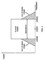
- FIG. 1 illustrates an ideal frequency spectrum of a typical CDMA signal.
- the vertical axis represents signal power, and the horizontal axis represents frequency.
- the desired in-band signal power is contained within the bandwidth defined by corner frequencies around a center frequency.
- a typical example is a 1.25 MHz bandwidth centered about a 1.96 GHz center frequency with corner frequencies at (1.96 GHz - 625 KHz) and (1.96 GHz + 625 KHz).
- the signal power drops significantly outside of the bandwidth, but some undesired out-of-band signal power is still present and is shaded on FIG. 1 .
- Out-of band signal power is undesirable because it represents wasted power that interferes with other signals in neighboring frequency bands.
- FIG. 2 illustrates a time domain plot of a typical CDMA signal.
- the vertical axis represents CDMA signal amplitude in volts, and the horizontal axis represents time.
- the dashed lines represent a maximum positive signal voltage (+Vmax) above the zero voltage point, and a negative maximum signal voltage (-Vmax) below the zero voltage point.
- the CDMA signal has "peaks" above and below the Vmax voltages. The peaks are shaded on FIG. 2 .
- FIG. 3 illustrates the operating characteristics of a typical power amplifier used to amplify a CDMA signal.
- the horizontal axis represents the input signal power (Pin), and the vertical axis represents the output signal power (Pout). If Pin is below a maximum power level (Pmax), then the power amplifier operates in a linear manner where an increase in Pin is matched by a proportional increase in Pout. If Pin is above Pmax, then the power amplifier operates in a nonlinear manner where an increase in Pin is not matched by a proportional increase in Pout. Pout is less than ideal in the nonlinear operating range.
- Vmax voltage levels on FIG. 2 correspond to the Pmax on FIG. 3 .
- the random signal peaks above +Vmax and below and -Vmax drive the power amplifier above Pmax into the nonlinear operating range.
- the power amplifier When operated in the nonlinear range, the power amplifier exhibits undesirable performance in the form of decreased fidelity and increased noise.
- the typical Frequency Modulated (FM) signal does not have random signal peaks, so the power amplifier is able to continuously operate below the maximum power level.
- the power amplifier generates additional out-of-band signal power when operated in the nonlinear range.
- Out-of-band signal power is a problem because it interferes with other signals in the neighboring frequency bands.
- Government agencies such as the Federal Communications Commission in the United States, strictly regulate the interference caused by out-of-band signal power.
- Test equipment is used to calculate a ratio for a test CDMA signal transmitted by the base station.
- the ratio represents the in-band signal power versus the out-of-band signal power.
- the base station transmit power is adjusted during the testing so the ratio is below a maximum value with a margin for some ratio increase under the maximum value.
- This usuallu Unfortunately the ratio is not calculated and is not used during normal base station operation in the field.
- Test equipment is used to calculate the ratio, and base stations are not equipped to calculate the ratio in the field. Thus, the ratio is not automatically generated and used to control operation in the field where changes in temperature and load alter base station operation.
- Another existing solution to this problem is to operate the CDMA base station so a ratio of the power out to the pilot signal does not exceed a value, such as five. This solution is lacking because a maximum power level based on the pilot signal is not an optimal estimate of the point where out-of-band signal power becomes a problem. As a result, the range and capacity of the base station is not optimized.
- FIG. 4 depicts a multi-sector base station 1100 that is currently known in the art.
- the base station 1100 is divided into geographic sectors with callers A-F in sector 1 and callers G-L in sector 2.
- caller F will move from sector 1 to sector 2 as indicated by the dashed lines, but the operation of the base station 1100 is first discussed prior to the caller F move from sector 1 to sector 2.
- the diagram of the base station 1100 has been simplified for clarity.
- the sector 1 portion of the base station 1100 includes cell site modems 1102 and 1104, gain control 1106, summing circuit 1108, CDMA signal processor 1110 including gain 1112, and antenna 1114.
- the sector 2 portion of the base station 1100 includes cell site modems 1122 and 1124, gain control 1126, summing circuit 1128, CDMA signal processor 1130 including gain 1132, and antenna 1134.
- the cell site modem 1102 receives signals for callers A, B, C and applies conventional CDMA processing to generate CDMA quadrature signals I and Q.
- the cell site modem 1102 provides the CDMA quadrature signals I and Q to the summing circuit 1108.
- the cell site modem 1104 receives signals for callers D, E, F and applies conventional CDMA processing to generate CDMA quadrature signals I and Q.
- the cell site modem 1104 provides the CDMA quadrature signals I and Q to the summing circuit 1108.
- the summing circuit separately combines the I signals and the Q signals and transfers them to the CDMA signal processor 1110.
- the CDMA signal processor 1110 performs analog conversion, filtering, up-conversion, and amplification to provide a Radio Frequency (RF) CDMA signal to the antenna 1114.
- the antenna 1114 transmits the RF CDMA signal 1116 over the air to the callers A-F in sector 1.
- the cell site modem 1122 receives signals for callers G, H, I and applies conventional CDMA processing to generate CDMA quadrature signals I and Q.
- the cell site modem 1122 provides the CDMA quadrature signals I and Q to the summing circuit 1128.
- the cell site modem 1124 receives signals for callers J, K, L and applies conventional CDMA processing to generate CDMA quadrature signals I and Q.
- the cell site modem 1124 provides the CDMA quadrature signals I and Q to the summing circuit 1128.
- the summing circuit separately combines the I signals and the Q signals and transfers them to the CDMA signal processor 1130.
- the CDMA signal processor 1130 performs analog conversion, filtering, up-conversion, and amplification to provide an RF CDMA signal to the antenna 1134.
- the antenna 1134 transmits the RF CDMA signal 1136 over the air to the callers G-L in sector 2.
- Each cell cite modem 1102, 1104, 1122, and 1124 provides gain information 1118 to both the gain control 1106 and the gain control 1126.
- the gain information 1118 includes the squared gain for each call, pilot signal, and overhead.
- Gain control 1106 and gain control 1126 each maintain a database that incorporates the gain information 1118.
- the CDMA signal processor 1110 monitors the transmit power (Pout) of the CDMA signal 1116 for sector 1 and provides a Pout value 1119 for sector 1 to the gain control 1106.
- the gain control 1106 compares the Pout value 1119 for the CDMA signal 1116 to a Gain Value (GV) equal to the sum of the squared gains for the CDMA signal 1116.
- the squared gains for the CDMA signal 1116 are obtained from the gain information 1118.
- the gain control 1106 transfers a control signal 1117 to the gain 1112 to adjust the Pout to maintain a ratio of GV to Pout at a pre-determined value.
- FIG. 5 shows the desired relationship between Pout and the GV.
- the points X and Y represent operational measurements, and the arrows represent the control applied through the control signal 1117 to the gain 1112 to maintain the pre-determined value.
- the slope of the pre-determined value blossoms during start-up and wilts during shut-down.
- the CDMA signal processor 1130 monitors the Pout for sector 2 and provides the Pout value 1139 for sector 2 to the gain control 1126.
- the gain control 1126 compares the Pout value 1139 for the CDMA signal 1136 to a GV equal to the sum of the squared gains for the CDMA signal 1136.
- the squared grains for the CDMA signal 1136 are obtained from the gain information 1118.
- the gain control 1126 transfers a control signal 1137 to the gain 1132 to adjust the Pout to maintain a ratio of GV to Pout at a pre-determined value.
- the cell site modem 1104 for sector 1 transfers the caller F quadrature signals 1141 and 1142 to the summing circuit 1128 for sector 2.
- the CDMA signal 1136 now includes the caller F signal.
- the gain control 1126 must now add the square of the caller F gain to its GV.
- each cell site modem must transfer all gain information 1118 to the gain control in each sector. This requires a data transfer arrangement across all sectors, and much of the transferred data is unnecessary. For example, gain control 1126 does not need the gain for caller A unless caller A moves into sector 2. The gain control for each sector must also track the calls in its sector and perform repeated calculations based on a changing database.
- CDMA systems would be improved by techniques to reduce the noise contribution of the power amplifier in the base station. The noise reduction would directly increase the power and efficiency of the CDMA base station. CDMA systems would also be improved through transmission at a power level just below the point where out-of-band signal power becomes a problem. Transmission at this power level would optimize the range and capacity of the base station. In addition, the current power calculation technique for CDMA base stations should be improved to reduce data transfer and storage.
- a digital base band section including the following: spread units for directly spreading input transmission data every channel by different spread codes to output spread signals, a summer for summing up the spread signals to output a multiplexed spread signal, a limiter for limiting an amplitude of the multiplexed spread signal not to exceed a predetermined value, and a roll-off filter that limits a transmission spectrum by shaping a waveform of the transmission signal to output a digital base band signal to an analog base band/RF section, where it is converted into an analog base band signal by a digital-to-analog converter and a carrier is modulated to convert the analog base band signal into an RF signal in a modulator, which RF signal is amplified in a transmission power amplifier to transmit the amplified RF signal through a transmission antenna.
- a device for processing a CDMA signal as set forth in claim 1, is provided.
- Embodiments of the invention are provided in the dependent claims.
- This technology can include decresting logic that reduces or eliminates random peaks in the CDMA signal.
- the power amplifier in a CDMA base station can then operate at increased power levels without exceeding out-of-band signal power limitations. Testing has shown a base station power increase of 3dB when decresting technology is used.
- the decresting logic generates a correction signal in response to peaks in the CDMA signal that exceed a threshold.
- the threshold typically corresponds to the maximum power level of a power amplifier.
- the decresting logic combines the correction signal with the CDMA signal to generate a decrested CDMA signal with reduced peaks.
- the decresting logic processes polar coordinate representations of the quadrature components of the CDMA signal to generate the correction signal.
- the transmission control technology includes spectral shaping logic that reduces the out-of-band signal power in the CDMA signal.
- the spectral shaping logic attenuates the in-band CDMA signal near the corner frequencies to reduce components that provide a disproportionate contribution to out-of-band signal power.
- the power amplifier in the CDMA base station can then operate at higher power levels without exceeding out-of-band signal power limitations.
- the transmission control technology includes ratio logic that allows a CDMA base station to operate at an optimized power level without generating improper amounts of out-of-band noise.
- Ratio logic automatically generates a ratio of the CDMA signal strength of the in-band components versus the out-of-band components to eliminate the need use pre-set margins for ratio increases in the field.
- the ratio logic uses the ratios to generate metric signals that indicate if transmit power should be limited and that indicate excess forward link capacity.
- the ratio logic uses the ratios to set the decresting threshold.
- the transmission control technology can include power control logic that controls the transmit power of the CDMA signal.
- the power control logic eliminates unnecessary data transfer and storage because gain control is accomplished without transferring or using per call gain information.
- the power control logic generates a ratio based on the power of the transmitted signal and a power value generated from quadrature components of the CDMA signal.
- the power control logic generates a power control signal based on the ratio. In some examples, the decresting logic provides the power value.
- the transmission control technology causes a CDMA base station to operate more efficiently.
- the transmission control technology also causes the CDMA base station to operate with a greater range or capacity. This improvement is passed on to the wireless communications user in the form of higher quality and lower cost.
- FIG. 6 depicts a baseband CDMA signal 600, a CDMA transmitter 601, an RF CDMA signal 602, and a CDMA receiver 603.
- CDMA is a spread-spectrum communications technology. Some versions of CDMA are specified by standards, such as IS-95 approved by the Telecommunications Industry Association.
- the CDMA signal 600 could be any CDMA signal, such as the signal produced by a cell site modem in a CDMA base station.
- the CDMA receiver 603 could be any CDMA device capable of receiving a CDMA signal, such as a wireless CDMA telephone.
- the CDMA transmitter 601 could be any CDMA transmission device that includes at least some of the functionality of transmit logic 610.
- This functionality includes decresting 611, in-band to out-of-band ratio (RIO) 612, power control 613, and spectral shaping 614.
- Decresting 611 reduces peaks in the CDMA signal 600.
- RIO 612 generates a ratio based on the signal strength of in-band versus out-of-band portions of the CDMA signal 602.
- Power control 613 adjusts the gain of the CDMA signal 602 based on quadrature signal calculations.
- Spectral shaping 614 attenuates in-band portions of the CDMA signal 600 adjacent to the corner frequencies.
- the CDMA transmitter 601 receives the CDMA signal 600.
- Decresting 611 generates a correction signal in response to peaks in the CDMA signal 600 that exceed a threshold.
- Decresting 611 then combines the correction signal with the CDMA signal 100 to generate a decrested CDMA signal with reduced peaks.
- the decrested signal is provided to spectral shaping 614.
- Spectral shaping 614 attenuates in-band portions of the decrested signal near the corner frequencies. The attenuation reduces the out-of-band noise caused by amplification of the CDMA signal. The attenuation should not be allowed to degrade the CDMA signal 602 to an unacceptable level.
- RIO 612 processes a copy of the CDMA signal 602 to generate the in-band to out-of-band signal ratios.
- the ratios are used to control the capacity and/or gain of the CDMA transmitter 601.
- the ratios can also are used to set the decresting threshold.
- Power control 613 processes quadrature components of the CDMA signal 600 to generate a gain control signal.
- the gain control signal is used to adjust the gain of the CDMA signal 602.
- the CDMA transmitter 601 transmits the CDMA signal 602 to the CDMA receiver 603 over the air interface.
- the invention is depicted using an air interface, other transmission media could also be used, such as RF cable, power lines, or telephone lines.
- FIG. 7 depicts a specific example of a CDMA system that uses transmit logic 723, but those skilled in the art will recognize numerous other types of CDMA systems that are applicable to the invention described above.
- FIG. 7 depicts a communications system 716 that is connected to a CDMA communications system 720.
- the CDMA communications system 720 communicates with CDMA communications devices 718.
- the CDMA communications system 720 is comprised of a switching center 721 and a base station 722.
- the communications system 716 exchanges communications signals 717 with the switching center 721.
- the switching center 721 exchanges communications signals 728 with the base station 722.
- the base station 722 exchanges wireless CDMA communications signals 719 over the air interface with the CDMA communications devices 718.
- the communications system 716 could be any communications system capable of exchanging communications signals 717 with the CDMA communications system 720.
- the communications system 716 is typically a conventional public telephone network, but could also be many other networks, such as a local area network, wide area network, or internet.
- the switching center 721 could be any device that provides an interface between the base station 722 and the communications system 716. Typically, numerous base stations are connected to the communications system 716 through the switching center 721, but the number of base stations has been restricted for the purpose of clarity.
- the base station 722 exchanges wireless CDMA signals 719 with the CDMA communications devices 718.
- the base station 722 includes transmit logic 723 that provides the functionality of the present invention.
- the functionality could include various combinations of the following: decresting 724, RIO 725, power control 726, and spectral shaping 727.
- numerous CDMA communications devices exchange signals with the base station 722, but the number of communications devices has been restricted for the purpose of clarity.
- Those skilled in the art could adapt the base station 722 from known systems, such as the base stations provided by Qualcomm, Inc. of San Diego, California.
- the CDMA communications devices 718 exchange wireless CDMA signals 719 with the base station 722.
- the typical CDMA communications device is a mobile telephone, but other CDMA communications devices are also possible, such as fixed wireless devices, data terminals, set-top boxes, or computers.
- the CDMA communications devices 718 communicate through the CDMA communications system 720 with the communications system 716 or with each other.
- the transmit logic 723 in the base station 722 operates on the communications path from the communications system 716 to the CDMA communications devices 718.
- FIG. 8 depicts the base station 722 of FIG. 7 receiving the communications signals 728 and transmitting the CDMA communications signals 719.
- the base station 722 could be a multi-sector base station with the components of FIG. 7 replicated for each sector.
- the base station 722 is comprised of the following elements connected in series: cell site modems 830, transmit logic 723, digital-to-analog converter and filter 831, up-converter 832, gain control 833, power amplifier 834, power monitor 835, and antenna 836. Aside from the transmit logic 723, those skilled in the art are familiar with these elements and their operation.
- the cell site modems 830 produce a CDMA signal comprised of quadrature signals 845 and 846.
- Quadrature CDMA signals are well-known and are baseband signals to be transmitted using carriers of the same frequency, but in phase quadrature.
- the cell site modems 830 may apply forward error correction coding before transferring the quadrature signals 845 and 846 to the transmit logic 723.
- the transmit logic 723 processes the quadrature signals 845 and 846 in accord with the invention and provides the resulting quadrature signals 847 and 848 to the digital-to-analog converter and filter 831.
- the transmit logic 723 receives also receives signals 840, 841, and provides signals 842, 843, 844, and 849. These signals and transmit logic 723 are described in detail further below.
- the digital-to-analog converter and filter 831 converts the quadrature signals 847 and 848 to analog and filters out components outside of the desired bandwidth.
- the digital-to-analog converter and filter 831 provides the analog quadrature signals to the up-converter 832.
- the up-converter 832 modulates the analog quadrature signals with intermediate and radio frequencies to form an RF CDMA signal and provides the RF CDMA signal to the gain control 833.
- the gain control 833 adjusts the gain of the RF CDMA signal based on the gain control signals 842, 843 and provides the gain-adjusted RF CDMA signal to the power amplifier 834.
- the power amplifier 834 amplifies the RF CDMA signal and provides the amplified RF CDMA signal to the power monitor 835.
- the power monitor 835 monitors the transmit power of the RF CDMA signal and provides signal 841 indicating transmit power to the transmit logic 723.
- the power monitor 835 provides the RF CDMA signal to the antenna 836.
- the antenna 836 transmits the RF CDMA signal 719
- FIG. 9 depicts the transmit logic 723 from FIGS. 7-8 .
- Transmit logic 723 includes various combinations of the following in various examples of the invention: decresting 724, RIO 725, power control 726, and spectral shaping 727.
- Decresting 724 receives the quadrature signals 845 and 846, which are referred to as Ia and Qa respectively.
- Decresting 724 processes the quadrature signals Ia and Qa to generate correction signals that correspond to signal peaks that exceed a threshold.
- the correction signals are combined with the quadrature signals Ia and Qa to eliminate or reduce the signal peaks.
- Decresting provides the resulting decrested quadrature signals Ib and Qb to spectral shaping 727.
- Spectral shaping 727 is comprised of digital filters that attenuate the strength of the in-band quadrature signals Ib and Qb to provide the shaped quadrature signals 847 and 848.
- RIO 725 receives the signal 840 which is a copy of the RF CDMA signal provided to the antenna 719 for transmission.
- RIO 725 processes the signal 840 to generate ratios of in-band to out-of-band signal strength. Signal strength can be measured in various ways with examples being power, voltage, or energy.
- RIO 725 compares the ratios to pre-determined values that represent the point where out-of-band signal power becomes improper.
- RIO 725 generates a capacity metric signal 842 and a power metric signal 843 based on the comparison. If one of the calculated ratios exceeds its associated pre-determined value, then the power metric signal 843 indicates that the transmit power of the base station 722 should be limited.
- the capacity metric signal 842 indicates an estimate of the excess forward link capacity of the base station 722. The estimate is typically given in a number of additional simultaneous calls that can be handled by the base station 722 without one of the calculated ratios exceeding its associated pre-determined value. RIO 725 also generates a threshold metric signal 953 based on the comparison.
- Power control 726 receives the signal 841 from the power monitor 835 and the signal 954 from decresting 724.
- the signal 841 indicates the power of the transmitted CDMA signal 719.
- the signal 954 indicates a power calculation using the quadrature signals 845 and 846.
- Power control 726 compares the signals 841 and 954 to generate the signals 844 and 849.
- the signal 844 is provided to the gain control 833 to adjust the gain. The gain is adjusted to maintain a pre-determined ratio of the signals 841 and 954.
- the signal 849 is a capacity control signal that indicates excess forward link capacity.
- the Vmax voltage levels on FIG. 2 correspond to the Pmax on FIG. 3 .
- the peaks above +Vmax and below and -Vmax would drive the power amplifier above Pmax into the nonlinear operating range.
- the power amplifier When operated in the nonlinear range, the power amplifier exhibits undesirable performance in the form of decreased fidelity and increased noise.
- the CDMA base station does not meet industry specifications, such as unused Walsh energy. Decresting eliminates or reduces the peaks to maintain operation of the power amplifier in the nonlinear range, and thus improves fidelity while reducing noise.
- FIG. 10 illustrates the frequency characteristics of a CDMA signal after decresting.
- the vertical axis represents signal power, and the horizontal axis represents frequency.
- the desired "in-band" signal power is contained within the bandwidth defined by corner frequencies that are above and below a center frequency.
- the signal power drops significantly outside of the bandwidth, but some undesired "out-of-band” signal power is still present, and is shaded on FIG. 10 .
- the dashed lines above the shaded out-of-band power on FIG. 10 represent the additional out-of-band signal power generated when decresting is not used.
- This additional out-of band signal power is undesirable because it represents wasted power that interferes with other signals in neighboring frequency bands.
- This reduction in out-of band signal power is typically offset by operating the power amplifier at a higher power level.
- the power amplifier has greater range or capacity at the higher power level, but does not generate intolerable out-of-band signal power.
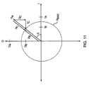
- FIG. 11 depicts representations of quadrature signals where the vertical axis represents values for Q quadrature signals, and the horizontal axis represents values for I quadrature signals.
- the time axis comes out of the page.
- the rectangular coordinate representations of the signals Qa, Qb, Ia, and Ib are indicated on the I axis and Q axis.
- Radius Ra and angle ⁇ show a polar coordinate representation of the quadrature signals Qa and Ia.
- Ra represents CDMA signal strength and exceeds a circle labeled Rmax. Other shapes could also be used with some examples being squares or diamonds.
- Rmax corresponds to the Vmax and the Pmax of FIGS. 2 and 3 respectively. Thus, the portion of Ra beyond Rmax represents a CDMA signal peak.
- a correction signal Rc would reduce Ra to the Rmax circle.
- Rc can be represented by quadrature correction signals Qc and Ic.
- Decresting is achieved by correcting the quadrature CDMA signals Qa and Ia with the quadrature correction signals Qc and Ic to generate the corrected quadrature CDMA signals Qb and Ib. Since decresting occurs in the digital domain, soft limiting is achieved that does not cause the undesired transients of hard limiting in the analog domain.
- the threshold Rmax can be set based on various factors, such as: 1) industry specifications for unused Walsh energy, 2) the RIO ratio of in-band to out-of-band signal power, 3) temperature -- lower during a cold start, 3) the Eb/Io ratio of bit energy to interference and noise, 4) the IS-97 industry standard Rho metric that is used to measure waveform fidelity, and/or 5) other suitable metrics.
- Rmax can be adjusted during system operation based on ongoing measurements of desired metrics and corresponding adjustment of Rmax to optimize performance.
- RIO can be periodically measured as Rmax is incrementally increased and decreased by a step-change. If RIO is lowered by an increased Rmax, then Rmax + delta become the new Rmax. If RIO is lowered by a decreased Rmax, then Rmax - delta become the new Rmax. Care should be taken to perform each of these tests under consistent conditions
- FIG. 12 depicts decresting 724.
- Decresting 724 receives the rectangular quadrature signals Ia and Qa and generates the corrected quadrature signals Ib and Qb.
- a rectangular-to-polar conversion element 1230 receives Ia and Qa and generates Ra and ⁇ .
- Subtraction element 1232 subtracts Ra from Rmax to generate Rc.
- Rc is negative if Ra exceeds Rmax, which occurs when a peak is encountered.
- Saturation element 1234 reduces positive values of Rc to zero.
- the saturation element 1234 provides Rc to the multiplication elements 1240 and 1242.
- the rectangular-to-polar conversion element 1230 also provides the signal 954 indicating the quadrature signal power calculation to power control 726.
- the conversion element 1230 also provides ⁇ to cosine element 1236 and sine element 1238.
- Cosine element 1236 and sine element 1238 respectively provide cosine ⁇ and sine ⁇ to the multiplication elements 1240 and 1242.
- the multiplication elements 1240 and 1242 multiply Rc with cosine ⁇ and sine ⁇ to respectively generate Ic and Qc.
- the multiplication elements 1240 and 1242 respectively provide Ic and Qc to filter elements 1244 and 1246.
- the filter elements 1244 and 1246 remove out-of-band components from Ic and Qc and respectively provide the signals to addition elements 1248 and 1250.
- the filtering elements could also remove some in-band components as well.
- the filtering is important because it converts decresting 723 from a clipping circuit or hard-limiter into a soft-limiter. Soft-limiting is important because it does not generate the unwanted transients that are produced by hard-limiting.
- Ia and Qa are respectively provided to time delay elements 1252 and 1254.
- the time delay elements 1252 and 1254 introduce a time delay that corresponds to the time required to generate Ic and Qc.
- the time delay elements 1252 and 1254 respectively provide Ia and Qa to the addition elements 1248 and 1250 so that they match in the time domain with Ic and Qc respectively.
- the addition element 1248 adds Ic to Ia to produce the corrected quadrature signal Ib.
- the addition element 1250 adds Qc to Qa to produce the corrected quadrature signal Qb.
- FIG. 13 depicts an alternative version of decresting 723. Essentially, a sampling element 1360 comprising circuitry 1362 and a low-pass filter 1364 is added in between the saturation element 1234 and the multiplication elements 1240 and 1242 on FIG. 12 . The remaining configuration and operation is unchanged from FIG. 12 .
- the saturation element 1234 provides Rc to the sampling element 1360.
- the circuitry 1362 samples Rc to detect a sample that exceeds the threshold and has the largest magnitude. This largest-magnitude sample represents a high point in the associated CDMA signal peak. The circuitry 1362 passes only this largest-magnitude sample that exceeds the threshold through the low-pass filter 1364.
- the sampling element 1360 provides the resulting Rc to the multiplication elements 1240 and 1242.
- the multiplication elements 1240 and 1242 multiply Rc with cosine ⁇ and sine ⁇ to respectively generate Ic and Qc.
- Ic and Qc are scaled versions of the negative impulse response of the lowpass filter 1364 in sampling element 1360. The scaling is such that the negative impulse responses, when added to the delayed signals Ia and Qa, will reduce the CDMA signal peak from Ra to Rmax.
- FIG. 14 depicts another alternative version of decresting 723.
- the quadrature logic 1470 replaces the elements 1230-1242 on FIG. 12 .
- the decresting 723 receives the rectangular quadrature signals Ia and Qa and generates the corrected quadrature signals Ib and Qb.
- Qc Qa ⁇ Rmax I ⁇ a 2 + Q ⁇ a 2 - 1 and positive bracketed terms are set to zero .
- the quadrature logic 1470 provides Ic and Qc to filter elements 1244 and 1246 respectively.
- the filter elements 1244 and 1246 remove out-of-band components from Ic and Qc and respectively provide the signals to addition elements 1248 and 1250.
- Ia and Qa are respectively provided to time delay elements 1252 and 1254.
- the time delay elements 1252 and 1254 introduce a time delay that corresponds to the time required to generate Ic and Qc.
- the time delay elements 1252 and 1254 respectively provide Ia and Qa to the addition elements 1248 and 1250 so that they match in the time domain with Ic and Qc respectively.
- the addition element 1248 adds Ic to Ia to produce the corrected in-phase signal Ib.
- the addition element 1250 adds Qc to Qa to produce the corrected in-phase signal Qb.
- a power amplifier is typically used to amplify CDMA signals.
- FIG. 15 illustrates the frequency spectrum of a CDMA signal that has been amplified after being shaped by spectral shaping 727.
- the vertical axis represents signal power, and the horizontal axis represents frequency.
- the desired in-band signal power is contained within the bandwidth defined by corner frequencies around a center frequency.
- the undesired out-of-band signal power is shaded on FIG. 15 .
- the dashed lines on FIG. 15 represent the CDMA signal from FIG. 1 that was not shaped by spectral shaping 727. The dashed lines illustrate that attenuation of the in-band signal power near the corner frequencies produces a reduction in the undesired out-of-band signal power.
- FIG. 16 depicts characteristics of the spectral shaping 727. Those skilled in the art recognize that FIG. 16 represents ideal characteristics, but will recognize how to configure spectral shaping 723 based on the ideal characteristics of FIG. 16 .
- the vertical axis represents signal strength, and the horizontal axis represents frequency.
- the dashed lines represent the CDMA signal before spectral shaping.
- Spectral shaping 727 could be comprised of a digital or analog band-pass filter with the following characteristics.
- the bandpass filter would attenuate the signal strength in the attenuation bandwidths (ABW) by attenuation (A), and pass the signal strength within the passband (PB).
- the attenuation bandwidths ABW are adjacent to the corner frequencies and in-band, so they are within the CDMA signal bandwidth (BW).
- the attenuation bandwidths (ABW) could each be 4.5% of the signal bandwidth BW.
- the passband PB could be 91% of the signal bandwidth BW and centered on the center frequency.
- the attenuation A could be 3 decibels.
- the spectral shaping can be implemented via baseband filtering prior to up-conversion.
- spectral shaping 727 is described with respect to FIG 8 .
- spectral shaping 727 is placed in the D/A converter and filter 831 in between the D/A converter and the filter components.
- Spectral shaping 727 would then be comprised of analog filters that attenuate the strength of the in-band quadrature signals I and Q near the corner frequencies as depicted in FIG. 16 .
- Spectral shaping 727 would then provide the shaped I and Q signals to the filter components of the D/A converter and filter 631. It may be desirable in this version of the invention to integrate spectral shaping 727 and these filter components into a single analog filter component combining the characteristics of the two.
- FIG. 17 depicts RIO 725.
- RIO 725 is comprised of down-converter 1772, transform logic 1773, and control logic 1774.
- the down-converter 1772 receives the signal 840 which is a copy of the transmitted CDMA signal.
- the down-converter 1772 de-modulates the RF signal 840 to form a baseband CDMA signal 1775.
- the down-converter 1772 provides the baseband CDMA signal 1775 to the transform logic 1773.
- FIG. 18 illustrates the frequency spectrum of the baseband CDMA signal 1775 received by the transform logic 1773.
- FIG. 18 is an ideal representation of the signal.
- the vertical axis represents signal power, and the horizontal axis represents frequency.
- the desired in-band signal power is contained within the bandwidth defined by corner frequencies around a center frequency.
- Bandwidth segments 1881-1887 are shown.
- Bandwidth segment 1881 is in-band, and bandwidth segments 1882-1887 are out-of-band.
- the power in each bandwidth segment 1881-1887 is shaded on FIG 18 .
- the segments depicted on FIG. 18 are shown for illustrative purposes, and the actual segments used could vary in number or bandwidth. The segments could also be determined based on industry standards
- the transform logic 1773 performs Fast-Fourier transforms to generate values representing the power in each bandwidth segment 1881-1887. Those skilled in the art are familiar with the logic required to perform such Fast-Fourier transforms. The transform logic 1773 then generates ratio values that will depend on the segments used. In this example, the following ratio values are generated:
- the transform logic 1773 generates a ratio signal 1776 that indicates the ratio values and transfers the ratio signal 1776 to the control logic 1774.
- the control logic 1774 compares each of the ratio values to an associated pre-determined maximum value for the particular ratio.
- the control logic 1774 determines if any of the calculated ratios exceed their respective maximum values.
- FIG. 19 depicts a logical table containing the ratio values 1-6, the respective maximum values, an indication if the ratios exceed the maximum values, and the difference between the ratios and the maximum values.
- the table is a logical representation that is capable of numerous implementations using conventional technology.
- the letters A-G that are listed in the table for the power ratio entries represent actual power measurements.
- the letters H-M that are listed in the table for the maximum value entries represent actual maximum values that can be readily obtained in standard industry publications, such as IS-97 by the Telecommunication Industry Association.
- the Federal Communications Commission also publishes maximum ratio values.
- the control logic 1774 generates the power metric signal 843 and transfers it to the gain control 833.
- the power metric signal 843 sets a flag in the gain control 833 if one of the ratios exceeds its maximum value.
- the flag causes the gain control 833 to limit the transmit power of the base station 722.
- the power metric signal 843 clears the flag when none of the ratios exceed their maximum values. In this fashion, the transmit power of the base station 722 is optimized to the point set by the maximum ratio values.
- the control logic 1774 generates a capacity metric signal 842 and transfers it to a base station control system (not shown).
- the capacity metric signal 842 indicates an estimate of the excess forward link capacity of the base station 722.
- the control logic 1774 determines the average difference between the measured ratios and the maximum values and translates the difference into a number of additional simultaneous calls that the base station 722 can handle without one of the calculated ratios exceeding its associated pre-determined value.
- the base station control system can determine whether or not to block call hand-offs or new calls based on the capacity metric signal 842. In this fashion, the number of simultaneous calls handled by the base station 722 is optimized to the point set by the maximum ratio values.
- the control logic 1774 also generates threshold metric signal 953 and transfers it to decresting 724.
- the threshold metric signal sets the threshold used by decresting 724.
- FIG. 20 depicts the power control 726.
- Power control 726 includes: ratio block 2090 and control block 2092.
- the ratio block 2090 receives signal 954 from decresting 724.
- the ratio block 2090 also receives the signal 841 from the power monitor 835.
- the signal 841 provides the value Pout which is the transmit power of the CDMA signal 719.
- the ratio block 2090 determines a ratio that equals R 2 / Pout.
- the ratio block 2090 provides the ratio in a signal 2091 to the control block 2092.
- the control block 2092 compares the ratio to a pre-determined value. Those skilled in the art are familiar with how to determine this pre-determined value by considering such factors as cell size, maximum rated power, minimum pilot signal strength at receiver, saturation, quantization errors, Ec/Io required at mobile device, and dynamic range of signal path.
- the control block 2092 generates the power control signal 844 to cause the gain control 833 to adjust the gain of the CDMA signal.
- the control block 2092 configures the power control signal 844 so the ratio moves closer to the pre-determined value.
- the control block 2092 also generates the capacity control signal 849 to indicate an estimate of the excess forward link capacity of the base station 722. The estimate is typically given in a number of additional simultaneous calls that can be handled by the base station 722.
- the control block 2092 transfers the capacity control signal 849 to a base station control system (not shown).
- FIG. 21 shows the desired relationship between Pout and the I 2 + Q 2 value.
- the points X and Y represent operational measurements, and the arrows represent the control applied through the control signal 844 to the gain control 833 to move the ratio closer to the pre-determined value.
- the slope of the pre-determined value blossoms during start-up and wilts during shut-down. Based on this document, those skilled in the art will appreciate how to assemble the power control 726 using conventional circuitry and software.
Landscapes
- Engineering & Computer Science (AREA)
- Computer Networks & Wireless Communication (AREA)
- Signal Processing (AREA)
- Mobile Radio Communication Systems (AREA)
- Transmitters (AREA)
Abstract
Claims (16)
- Dispositif (601) pour le traitement d'un signal d'Accès Multiple par Différence de Code (CDMA), le dispositif comprenant :une logique d'écrêtage (611) actionnable pour réduire des pics dépassant un seuil dans le signal CDMA ;une logique de mise en forme spectrale (614) actionnable pour atténuer des fréquences dans la bande du signal CDMA ; etune logique de rapport (612) actionnable pour générer automatiquement un rapport d'intensité entre au moins une partie des composantes dans la bande dans le signal CDMA et au moins une partie des composantes hors-bande dans le signal CDMA.
- Dispositif (601) selon la revendication 1, dans lequel la logique d'écrêtage (611) est en outre actionnable pour générer un signal de correction numérique en réponse aux pics et pour combiner le signal de correction numérique avec une version numérique du signal CDMA.
- Dispositif (601) selon la revendication 2, dans lequel la logique d'écrêtage (611) est en outre actionnable pour générer le signal de correction en traitant une représentation en coordonnées polaires de composantes en quadrature du signal CDMA.
- Dispositif (601) selon la revendication 1, dans lequel la logique de mise en forme spectrale (614) est en outre actionnable pour atténuer les fréquences dans la bande qui sont adjacentes à une première fréquence pivot et adjacentes à une deuxième fréquence pivot, les fréquences pivots définissant une largeur de bande du signal CDMA.
- Dispositif (601) selon la revendication 1, dans lequel la logique de rapport (612) est en outre actionnable pour générer un signal de métrique pour limiter la puissance d'émission sur la base dudit rapport.
- Dispositif (601) selon la revendication 1, dans lequel la logique de rapport (612) est en outre actionnable pour générer un signal de métrique indiquant un excès de capacité en liaison directe sur la base du rapport.
- Dispositif (601) selon la revendication 1, dans lequel la logique de rapport (612) est en outre actionnable pour régler le seuil sur la base dudit rapport.
- Dispositif (601) selon la revendication 1, comprenant en outre de la logique de commande de puissance (613) actionnable pour comparer une valeur de puissance, calculée à partir de composantes en quadrature du signal CDMA, avec une puissance d'émission du signal CDMA, et pour ajuster automatiquement un gain du signal CDMA sur la base de la comparaison.
- Dispositif (601) selon la revendication 8, dans lequel la logique d'écrêtage (611) est en outre actionnable pour calculer la valeur de puissance.
- Dispositif (601) selon la revendication 8, comprenant en outre un dispositif de surveillance de puissance (635) actionnable pour surveiller la puissance d'émission du signal CDMA.
- Dispositif (601) selon la revendication 8, comprenant en outre un modem de site cellulaire (830) actionnable pour générer le signal CDMA.
- Dispositif (601) selon la revendication 8, comprenant en outre un convertisseur numérique-vers-analogique (821) actionnable pour convertir le signal CDMA du domaine numérique vers le domaine analogique.
- Dispositif (601) selon la revendication 8, comprenant en outre un filtre passe-bas actionnable pour atténuer du bruit hors-bande dans le signal CDMA.
- Dispositif (601) selon la revendication 8, comprenant en outre un élévateur de fréquence (832) actionnable pour moduler le signal CDMA vers une fréquence radio.
- Dispositif (601) selon la revendication 8, comprenant en outre un amplificateur de puissance (834) actionnable pour amplifier le signal CDMA.
- Dispositif (601) selon la revendication 8, comprenant en outre une antenne (836) actionnable pour émettre le signal CDMA.
Applications Claiming Priority (3)
| Application Number | Priority Date | Filing Date | Title |
|---|---|---|---|
| US265204 | 1988-10-31 | ||
| US09/265,204 US6687238B1 (en) | 1999-03-10 | 1999-03-10 | CDMA signal transmission control |
| PCT/US2000/006227 WO2000054428A1 (fr) | 1999-03-10 | 2000-03-10 | Commande d'emission de signaux amdc |
Publications (2)
| Publication Number | Publication Date |
|---|---|
| EP1157481A1 EP1157481A1 (fr) | 2001-11-28 |
| EP1157481B1 true EP1157481B1 (fr) | 2012-02-08 |
Family
ID=23009468
Family Applications (1)
| Application Number | Title | Priority Date | Filing Date |
|---|---|---|---|
| EP00914896A Expired - Lifetime EP1157481B1 (fr) | 1999-03-10 | 2000-03-10 | Commande d'emission de signaux amdc |
Country Status (9)
| Country | Link |
|---|---|
| US (1) | US6687238B1 (fr) |
| EP (1) | EP1157481B1 (fr) |
| KR (1) | KR100649290B1 (fr) |
| CN (1) | CN1172454C (fr) |
| AU (1) | AU3622400A (fr) |
| BR (1) | BR0008810A (fr) |
| CA (1) | CA2364375C (fr) |
| HK (1) | HK1042795B (fr) |
| WO (1) | WO2000054428A1 (fr) |
Families Citing this family (19)
| Publication number | Priority date | Publication date | Assignee | Title |
|---|---|---|---|---|
| US6931053B2 (en) | 1998-11-27 | 2005-08-16 | Nortel Networks Limited | Peak power and envelope magnitude regulators and CDMA transmitters featuring such regulators |
| US6943678B2 (en) * | 2000-01-24 | 2005-09-13 | Nextreme, L.L.C. | Thermoformed apparatus having a communications device |
| US7342496B2 (en) | 2000-01-24 | 2008-03-11 | Nextreme Llc | RF-enabled pallet |
| US8077040B2 (en) * | 2000-01-24 | 2011-12-13 | Nextreme, Llc | RF-enabled pallet |
| JP3478496B2 (ja) * | 2000-11-24 | 2003-12-15 | 松下電器産業株式会社 | 送信電力制御方法及びその装置並びに通信装置 |
| US8331490B2 (en) * | 2001-10-22 | 2012-12-11 | Panasonic Corporation | Methods and apparatus for conditioning communications signals based on detection of high-frequency events in polar domain |
| US20070211829A1 (en) * | 2001-10-22 | 2007-09-13 | Matsushita Electric Industrial Co., Ltd. | Method and apparatus for pulse optimization for non-linear filtering |
| US7054385B2 (en) * | 2001-10-22 | 2006-05-30 | Tropian, Inc. | Reduction of average-to-minimum power ratio in communications signals |
| FR2832569B1 (fr) * | 2001-11-22 | 2007-04-27 | Evolium Sas | Procede de transmission de communications dans un systeme de telecommunication de type cellulaire utilisant des bandes de frequences porteuses adjacentes |
| US7151795B1 (en) * | 2001-12-31 | 2006-12-19 | Arraycomm Llc | Method and apparatus for increasing spectral efficiency using mitigated power near band-edge |
| US7133375B1 (en) * | 2002-03-05 | 2006-11-07 | Sprint Spectrum L.P. | Dynamic adaptive multifunctional base station for wireless networks |
| JP4110385B2 (ja) * | 2002-12-02 | 2008-07-02 | 日本電気株式会社 | 電力制限器 |
| KR20050090283A (ko) * | 2004-03-08 | 2005-09-13 | 엘지전자 주식회사 | 다운로드 받은 음악파일의 이득조정방법 |
| US7995975B2 (en) * | 2006-12-21 | 2011-08-09 | Telefonaktiebolaget Lm Ericsson (Publ) | Method and apparatus for signal peak-to-average ratio reduction |
| US8462757B2 (en) * | 2008-12-15 | 2013-06-11 | Intel Mobile Communications GmbH | Method for adjusting transmitter output power |
| JP5212402B2 (ja) * | 2010-02-24 | 2013-06-19 | 住友電気工業株式会社 | ピーク電力抑制回路とこの回路を有する通信装置 |
| US8411771B2 (en) | 2010-05-19 | 2013-04-02 | Qualcomm Incorporated | Predictive clipping in multi-carrier wireless communication systems |
| WO2014046582A1 (fr) * | 2012-09-21 | 2014-03-27 | Telefonaktiebolaget L M Ericsson (Publ) | Procédé et nœud de réseau radio pour commander l'émission de signaux par le nœud de réseau radio |
| WO2017144079A1 (fr) * | 2016-02-23 | 2017-08-31 | Telefonaktiebolaget Lm Ericsson (Publ) | Procédé et système de test par radio d'émissions indésirables |
Family Cites Families (9)
| Publication number | Priority date | Publication date | Assignee | Title |
|---|---|---|---|---|
| US5297161A (en) * | 1992-06-29 | 1994-03-22 | Motorola Inc. | Method and apparatus for power estimation in an orthogonal coded communication system |
| US5412686A (en) * | 1993-09-17 | 1995-05-02 | Motorola Inc. | Method and apparatus for power estimation in a communication system |
| US5742595A (en) * | 1995-06-02 | 1998-04-21 | Dsc Communications Corporation | Processing CDMA signals |
| JP2718398B2 (ja) * | 1995-06-30 | 1998-02-25 | 日本電気株式会社 | Cdma基地局送信装置 |
| KR100212053B1 (ko) * | 1995-12-30 | 1999-08-02 | 윤종용 | 기지국 송출전력 자동 제어 장치 및 방법 |
| US5978362A (en) * | 1996-02-06 | 1999-11-02 | Airtouch Communications, Inc. | Method and apparatus for eliminating intermodulation interference in cellular telephone systems |
| KR100193848B1 (ko) * | 1996-10-05 | 1999-06-15 | 윤종용 | 대역확산통신기에 있어서 수신신호 이득 자동제어장치 및 방법 |
| US6094585A (en) * | 1997-11-14 | 2000-07-25 | Lucent Technologies Inc. | CDMA forward link power overload control in a base station |
| KR100289284B1 (ko) * | 1997-12-27 | 2001-05-02 | 박종섭 | 이동통신 시스템 기지국의 순방향 전력제어장치 및 그 제어방법 |
-
1999
- 1999-03-10 US US09/265,204 patent/US6687238B1/en not_active Expired - Lifetime
-
2000
- 2000-03-10 CA CA002364375A patent/CA2364375C/fr not_active Expired - Fee Related
- 2000-03-10 CN CNB00804855XA patent/CN1172454C/zh not_active Expired - Lifetime
- 2000-03-10 KR KR1020017011490A patent/KR100649290B1/ko not_active IP Right Cessation
- 2000-03-10 AU AU36224/00A patent/AU3622400A/en not_active Abandoned
- 2000-03-10 WO PCT/US2000/006227 patent/WO2000054428A1/fr active IP Right Grant
- 2000-03-10 EP EP00914896A patent/EP1157481B1/fr not_active Expired - Lifetime
- 2000-03-10 BR BR0008810-2A patent/BR0008810A/pt not_active IP Right Cessation
-
2002
- 2002-06-10 HK HK02104335.4A patent/HK1042795B/zh not_active IP Right Cessation
Also Published As
| Publication number | Publication date |
|---|---|
| AU3622400A (en) | 2000-09-28 |
| HK1042795A1 (en) | 2002-08-23 |
| KR100649290B1 (ko) | 2006-11-24 |
| KR20020016763A (ko) | 2002-03-06 |
| CA2364375A1 (fr) | 2000-09-14 |
| US6687238B1 (en) | 2004-02-03 |
| BR0008810A (pt) | 2003-03-05 |
| EP1157481A1 (fr) | 2001-11-28 |
| CA2364375C (fr) | 2009-01-06 |
| CN1343399A (zh) | 2002-04-03 |
| HK1042795B (zh) | 2005-05-13 |
| WO2000054428A1 (fr) | 2000-09-14 |
| CN1172454C (zh) | 2004-10-20 |
Similar Documents
| Publication | Publication Date | Title |
|---|---|---|
| EP1157481B1 (fr) | Commande d'emission de signaux amdc | |
| EP1388937B1 (fr) | Amplificateur radiofréquence comprenant un limiteur adaptatif | |
| EP1398886B1 (fr) | Alimentation dynamique pour un amplificateur de puissance | |
| EP1195034B1 (fr) | Schema de regulation de puissance pour maximiser le rapport signal/bruit des porteuses dans des emetteurs a plusieurs porteuses | |
| US7340224B2 (en) | Devices for reducing the dynamic range of signals in transmitters of communication systems | |
| US7489907B2 (en) | Transmitter for suppressing a variation in input level of a multicarrier signal | |
| US20050017801A1 (en) | Elimination of peak clipping and improved efficiency for RF power amplifiers with a predistorter | |
| JP2000307549A (ja) | 基地局装置及びピーク電力抑圧方法 | |
| US6370109B1 (en) | CDMA signal power control using quadrature signal calculations | |
| EP1360760B1 (fr) | Limitation d'amplitude | |
| CN101150357A (zh) | 削除峰值功率的方法 | |
| US6515961B1 (en) | Decresting peaks in a CDMA signal | |
| US7570709B2 (en) | Automatic transmit power control loop with modulation averaging | |
| US6430169B1 (en) | Spectral shaping a CDMA signal | |
| US20030219079A1 (en) | Data transmission method and arrangement | |
| KR100649922B1 (ko) | 대역내 및 대역외 신호의 비를 이용한 cdma 신호의 송신 | |
| Linde et al. | Power and spectral efficiency of a family of constant-envelope root-of-unity filtered complex spreading sequences in WCDMA non-linear power amplification |
Legal Events
| Date | Code | Title | Description |
|---|---|---|---|
| PUAI | Public reference made under article 153(3) epc to a published international application that has entered the european phase |
Free format text: ORIGINAL CODE: 0009012 |
|
| 17P | Request for examination filed |
Effective date: 20010907 |
|
| AK | Designated contracting states |
Kind code of ref document: A1 Designated state(s): AT BE CH CY DE DK ES FI FR GB GR IE IT LI LU MC NL PT SE |
|
| AX | Request for extension of the european patent |
Free format text: AL;LT;LV;MK;RO;SI |
|
| RIN1 | Information on inventor provided before grant (corrected) |
Inventor name: PRESSLEY, TODD, A. Inventor name: FUNK, THOMAS, J. Inventor name: FLOWERS, LARRY, D. Inventor name: SOONG, ANTHONY, C., K. Inventor name: WEAVER, LINDSAY, A., JR. Inventor name: HARMS, BRIAN, K. Inventor name: SCHWARTZ, BRUCE, S. |
|
| RIN1 | Information on inventor provided before grant (corrected) |
Inventor name: SOONG, ANTHONY, C., K. Inventor name: FUNK, THOMAS, J. Inventor name: WEAVER, LINDSAY, A., JR. Inventor name: HARMS, BRIAN, K. Inventor name: FLOWERS, LARRY, D. C/O QUALCOMM INCORPORATED Inventor name: PRESSLEY, TODD, A. Inventor name: SCHWARTZ, BRUCE, S. |
|
| RBV | Designated contracting states (corrected) |
Designated state(s): DE FI FR GB IT SE |
|
| 17Q | First examination report despatched |
Effective date: 20060222 |
|
| RIN1 | Information on inventor provided before grant (corrected) |
Inventor name: FLOWERS, LARRY, D.C/O QUALCOMM INCORPORATED Inventor name: HARMS, BRIAN, K. Inventor name: SCHWARTZ, BRUCE, S. Inventor name: KNIGHT, ROBIN, D. Inventor name: WEAVER, LINDSAY, A., JR. Inventor name: SOONG, ANTHONY, C., K. Inventor name: PRESSLEY, TODD, A. Inventor name: FUNK, THOMAS, J. |
|
| GRAP | Despatch of communication of intention to grant a patent |
Free format text: ORIGINAL CODE: EPIDOSNIGR1 |
|
| GRAS | Grant fee paid |
Free format text: ORIGINAL CODE: EPIDOSNIGR3 |
|
| GRAA | (expected) grant |
Free format text: ORIGINAL CODE: 0009210 |
|
| AK | Designated contracting states |
Kind code of ref document: B1 Designated state(s): DE FI FR GB IT SE |
|
| REG | Reference to a national code |
Ref country code: GB Ref legal event code: FG4D |
|
| REG | Reference to a national code |
Ref country code: DE Ref legal event code: R096 Ref document number: 60046911 Country of ref document: DE Effective date: 20120405 |
|
| PG25 | Lapsed in a contracting state [announced via postgrant information from national office to epo] |
Ref country code: FI Free format text: LAPSE BECAUSE OF FAILURE TO SUBMIT A TRANSLATION OF THE DESCRIPTION OR TO PAY THE FEE WITHIN THE PRESCRIBED TIME-LIMIT Effective date: 20120208 |
|
| PG25 | Lapsed in a contracting state [announced via postgrant information from national office to epo] |
Ref country code: SE Free format text: LAPSE BECAUSE OF FAILURE TO SUBMIT A TRANSLATION OF THE DESCRIPTION OR TO PAY THE FEE WITHIN THE PRESCRIBED TIME-LIMIT Effective date: 20120208 |
|
| PG25 | Lapsed in a contracting state [announced via postgrant information from national office to epo] |
Ref country code: IT Free format text: LAPSE BECAUSE OF FAILURE TO SUBMIT A TRANSLATION OF THE DESCRIPTION OR TO PAY THE FEE WITHIN THE PRESCRIBED TIME-LIMIT Effective date: 20120208 |
|
| PLBE | No opposition filed within time limit |
Free format text: ORIGINAL CODE: 0009261 |
|
| STAA | Information on the status of an ep patent application or granted ep patent |
Free format text: STATUS: NO OPPOSITION FILED WITHIN TIME LIMIT |
|
| REG | Reference to a national code |
Ref country code: FR Ref legal event code: ST Effective date: 20121130 |
|
| 26N | No opposition filed |
Effective date: 20121109 |
|
| PG25 | Lapsed in a contracting state [announced via postgrant information from national office to epo] |
Ref country code: FR Free format text: LAPSE BECAUSE OF NON-PAYMENT OF DUE FEES Effective date: 20120410 |
|
| REG | Reference to a national code |
Ref country code: DE Ref legal event code: R097 Ref document number: 60046911 Country of ref document: DE Effective date: 20121109 |
|
| PGFP | Annual fee paid to national office [announced via postgrant information from national office to epo] |
Ref country code: GB Payment date: 20170223 Year of fee payment: 18 |
|
| PGFP | Annual fee paid to national office [announced via postgrant information from national office to epo] |
Ref country code: DE Payment date: 20170711 Year of fee payment: 18 |
|
| REG | Reference to a national code |
Ref country code: DE Ref legal event code: R119 Ref document number: 60046911 Country of ref document: DE |
|
| GBPC | Gb: european patent ceased through non-payment of renewal fee |
Effective date: 20180310 |
|
| PG25 | Lapsed in a contracting state [announced via postgrant information from national office to epo] |
Ref country code: DE Free format text: LAPSE BECAUSE OF NON-PAYMENT OF DUE FEES Effective date: 20181002 |
|
| PG25 | Lapsed in a contracting state [announced via postgrant information from national office to epo] |
Ref country code: GB Free format text: LAPSE BECAUSE OF NON-PAYMENT OF DUE FEES Effective date: 20180310 |