EP1156521A2 - Low cost electroless plating process for single chips and wafer parts and products obtained thereof - Google Patents
Low cost electroless plating process for single chips and wafer parts and products obtained thereof Download PDFInfo
- Publication number
- EP1156521A2 EP1156521A2 EP01870087A EP01870087A EP1156521A2 EP 1156521 A2 EP1156521 A2 EP 1156521A2 EP 01870087 A EP01870087 A EP 01870087A EP 01870087 A EP01870087 A EP 01870087A EP 1156521 A2 EP1156521 A2 EP 1156521A2
- Authority
- EP
- European Patent Office
- Prior art keywords
- carrier
- wafer
- recited
- plating
- semiconductor chip
- Prior art date
- Legal status (The legal status is an assumption and is not a legal conclusion. Google has not performed a legal analysis and makes no representation as to the accuracy of the status listed.)
- Ceased
Links
Images




Classifications
-
- H—ELECTRICITY
- H10—SEMICONDUCTOR DEVICES; ELECTRIC SOLID-STATE DEVICES NOT OTHERWISE PROVIDED FOR
- H10P—GENERIC PROCESSES OR APPARATUS FOR THE MANUFACTURE OR TREATMENT OF DEVICES COVERED BY CLASS H10
- H10P14/00—Formation of materials, e.g. in the shape of layers or pillars
- H10P14/40—Formation of materials, e.g. in the shape of layers or pillars of conductive or resistive materials
- H10P14/46—Formation of materials, e.g. in the shape of layers or pillars of conductive or resistive materials using a liquid
-
- H—ELECTRICITY
- H10—SEMICONDUCTOR DEVICES; ELECTRIC SOLID-STATE DEVICES NOT OTHERWISE PROVIDED FOR
- H10P—GENERIC PROCESSES OR APPARATUS FOR THE MANUFACTURE OR TREATMENT OF DEVICES COVERED BY CLASS H10
- H10P72/00—Handling or holding of wafers, substrates or devices during manufacture or treatment thereof
- H10P72/70—Handling or holding of wafers, substrates or devices during manufacture or treatment thereof for supporting or gripping
- H10P72/74—Handling or holding of wafers, substrates or devices during manufacture or treatment thereof for supporting or gripping using temporarily an auxiliary support
-
- H—ELECTRICITY
- H10—SEMICONDUCTOR DEVICES; ELECTRIC SOLID-STATE DEVICES NOT OTHERWISE PROVIDED FOR
- H10W—GENERIC PACKAGES, INTERCONNECTIONS, CONNECTORS OR OTHER CONSTRUCTIONAL DETAILS OF DEVICES COVERED BY CLASS H10
- H10W72/00—Interconnections or connectors in packages
- H10W72/01—Manufacture or treatment
- H10W72/012—Manufacture or treatment of bump connectors, dummy bumps or thermal bumps
- H10W72/01215—Manufacture or treatment of bump connectors, dummy bumps or thermal bumps forming coatings
-
- H—ELECTRICITY
- H10—SEMICONDUCTOR DEVICES; ELECTRIC SOLID-STATE DEVICES NOT OTHERWISE PROVIDED FOR
- H10W—GENERIC PACKAGES, INTERCONNECTIONS, CONNECTORS OR OTHER CONSTRUCTIONAL DETAILS OF DEVICES COVERED BY CLASS H10
- H10W72/00—Interconnections or connectors in packages
- H10W72/01—Manufacture or treatment
- H10W72/012—Manufacture or treatment of bump connectors, dummy bumps or thermal bumps
- H10W72/01251—Changing the shapes of bumps
- H10W72/01255—Changing the shapes of bumps by using masks
-
- H—ELECTRICITY
- H10—SEMICONDUCTOR DEVICES; ELECTRIC SOLID-STATE DEVICES NOT OTHERWISE PROVIDED FOR
- H10W—GENERIC PACKAGES, INTERCONNECTIONS, CONNECTORS OR OTHER CONSTRUCTIONAL DETAILS OF DEVICES COVERED BY CLASS H10
- H10W72/00—Interconnections or connectors in packages
- H10W72/20—Bump connectors, e.g. solder bumps or copper pillars; Dummy bumps; Thermal bumps
- H10W72/221—Structures or relative sizes
- H10W72/222—Multilayered bumps, e.g. a coating on top and side surfaces of a bump core
- H10W72/223—Multilayered bumps, e.g. a coating on top and side surfaces of a bump core characterised by the structure of the outermost layers, e.g. multilayered coatings
-
- H—ELECTRICITY
- H10—SEMICONDUCTOR DEVICES; ELECTRIC SOLID-STATE DEVICES NOT OTHERWISE PROVIDED FOR
- H10W—GENERIC PACKAGES, INTERCONNECTIONS, CONNECTORS OR OTHER CONSTRUCTIONAL DETAILS OF DEVICES COVERED BY CLASS H10
- H10W72/00—Interconnections or connectors in packages
- H10W72/20—Bump connectors, e.g. solder bumps or copper pillars; Dummy bumps; Thermal bumps
- H10W72/251—Materials
- H10W72/252—Materials comprising solid metals or solid metalloids, e.g. PbSn, Ag or Cu
-
- H—ELECTRICITY
- H10—SEMICONDUCTOR DEVICES; ELECTRIC SOLID-STATE DEVICES NOT OTHERWISE PROVIDED FOR
- H10W—GENERIC PACKAGES, INTERCONNECTIONS, CONNECTORS OR OTHER CONSTRUCTIONAL DETAILS OF DEVICES COVERED BY CLASS H10
- H10W72/00—Interconnections or connectors in packages
- H10W72/20—Bump connectors, e.g. solder bumps or copper pillars; Dummy bumps; Thermal bumps
- H10W72/251—Materials
- H10W72/255—Materials of outermost layers of multilayered bumps, e.g. material of a coating
-
- H—ELECTRICITY
- H10—SEMICONDUCTOR DEVICES; ELECTRIC SOLID-STATE DEVICES NOT OTHERWISE PROVIDED FOR
- H10W—GENERIC PACKAGES, INTERCONNECTIONS, CONNECTORS OR OTHER CONSTRUCTIONAL DETAILS OF DEVICES COVERED BY CLASS H10
- H10W72/00—Interconnections or connectors in packages
- H10W72/90—Bond pads, in general
-
- H—ELECTRICITY
- H10—SEMICONDUCTOR DEVICES; ELECTRIC SOLID-STATE DEVICES NOT OTHERWISE PROVIDED FOR
- H10W—GENERIC PACKAGES, INTERCONNECTIONS, CONNECTORS OR OTHER CONSTRUCTIONAL DETAILS OF DEVICES COVERED BY CLASS H10
- H10W72/00—Interconnections or connectors in packages
- H10W72/90—Bond pads, in general
- H10W72/941—Dispositions of bond pads
- H10W72/9415—Dispositions of bond pads relative to the surface, e.g. recessed, protruding
-
- H—ELECTRICITY
- H10—SEMICONDUCTOR DEVICES; ELECTRIC SOLID-STATE DEVICES NOT OTHERWISE PROVIDED FOR
- H10W—GENERIC PACKAGES, INTERCONNECTIONS, CONNECTORS OR OTHER CONSTRUCTIONAL DETAILS OF DEVICES COVERED BY CLASS H10
- H10W72/00—Interconnections or connectors in packages
- H10W72/90—Bond pads, in general
- H10W72/951—Materials of bond pads
- H10W72/952—Materials of bond pads comprising metals or metalloids, e.g. PbSn, Ag or Cu
Definitions
- the present invention is related to a method for under-bump-metallisation (UBM) of single chips, dice, wafer parts or wafers.
- UBM under-bump-metallisation
- the under-bump-metallisation is formed by electroless plating of the bonding pads.
- top layer e.g. an aluminium alloy
- additional steps are required to modify the top layer, e.g. an aluminium alloy, of the bond pads and/or to add layers to these bond pads as such aluminium alloy top layers cannot be soldered or glued.
- additional steps comprise the use of, for example, electroless Nickel/ immersion Gold (e-Ni/Au) plating as a bond pad-finishing step prior to the flip-chip assembly.
- the UBM forms an interface between the bonding pads and the solder bumps and provides adhesion, forms a diffusion barrier and offers solder wettable layers. After formation of the UBM, solder bumps can be formed on the bonding pads by various methods, such as electroplating.
- a present method of plating bond pads of a single chip is to deposit on the edges and on the backside of the chip or wafer part a photoresist layer.
- This technique is already used for electroless plating of entire wafers in order to form the UBM.
- the backside of the wafer is covered with a resist layer to avoid plating on this region. Because the area of the backside is large compared to the total area of the bonding pads to be plated, plating the backside would consume a major part of the metal, e.g. the nickel, present in the plating solution. This excess and unwanted consumption of nickel would substantially decrease the lifetime of the plating bath.
- nickel grown on the back side of the silicon substrate will adhere poorly to this silicon surface and may be lifted off during subsequent processing. Therefore, the back side of single chips is covered with a resist layer.
- the application of this wafer-scale technique to the formation of UBM on single dice is done manually and is therefore a time consuming and expensive processing step.
- This bonding step includes the step of executing a thermocompression cycle and requires high temperatures and a holding force to obtain a bond that withstands the plating process.
- the release of the plated chip further requires additional heating steps.
- Finally time-consuming cleaning steps were required to remove all residues of the amorphous thermoplastic adhesive on the backside after debonding. So far, no successful attempts to plate single chips or wafer parts in a low cost way on a commercial basis have been reported.
- An aim of the invention is to offer a method for forming under-bump-metallurgy on all bonding pads of a single chip, die, wafer part or wafer. These bonding pads include the bonding pads connected with the ground plane or small bond pads.
- An aim of the present invention is to offer a method to uniform plate bonding pads on singulated chips, single dice, wafer parts or wafers in a much more simple and cost-effective way.
- An aim of the present invention is to offer a method to apply commercially available electroless plating procedures to uniformally plate bonding pads on singulated chips, single dice, wafer parts or wafers in a much more simple and cost-effective way.
- An aim of the present invention is to simplify and to ease the handling of the singulated chips, single dice, wafer parts or wafers during the formation of the UBM.
- the formation of the UBM is done by electroless plating.
- An aim of the present invention is to offer a simple and cost-effective method to plate bonding pads of a single chip substantial uniformly and to avoid plating on a major part of this single chip.
- a method to plate bond pads in case of comprises the steps of attaching the singulated chip, single die, wafer part, or wafer to a non-conductive substrate or non-conductive adhesive layer.
- the plating of the bond pads can be made uniform and in all dimensions.
- the adhesive layer is a pressure-sensitive adhesive.
- the pressure sensitive adhesive is preferably a removable pressure sensitive adhesive.
- a removable pressure sensitive adhesive is characterized by low ultimate adhesion to a wide variety of surfaces.
- the pressure sensitive adhesive preferably leaves no residue when removed from a substrate such as a semiconductor substrate.
- the pressure sensitive adhesive preferably has a cure or melt temperature above the process temperature of the plating bath. This cure or melt temperature is preferably higher than 100° C.
- adhesive is used to attach the single die, wafer part or wafer to a temporary carrier, such as a tape or sheet. The adhesive may be pre-applied to the sheet or to the single die, wafer part or wafer.
- the plating bath used is an electroless plating bath.
- This electroless plating bath is a preferably self-catalytic plating bath.
- a nickel plating bath is used to form the UBM.
- the non-conductive substrate has a cure or melt temperature above the process temperature of the plating bath. Preferably this cure or melt temperature is higher than 100C.
- a polyamide carrier is used as non-conductive substrate.
- the present invention may also provide a method for electroless plating individual semiconductor chips with bonding pads comprising the steps of: attaching the individual semiconductor chip to a carrier, electroless plating the bond pads of said individual semiconductor chip, detaching the individual semiconductor chip from the carrier, wherein said step of attaching the individual semiconductor chip to the carrier comprises the steps of: forming a semiconductor wafer having two major surfaces, the bonding pads being located on one major surface, forming an insulating layer at least on the other major surface of the wafer, dicing the semiconductor wafer into individual chips.
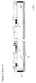
- a commercially available electroless nickel/gold plating process consists of the following steps (see figure 1):
- edges i.e. backside (11) and bevels or side edges (14), electrically isolated from the plating bath (see figure 2).
- layers (8) e.g. chemical vapour deposited (CVD) oxides, formed on the wafer surface during the process of creating the electronic circuitry.
- the backside (11) of the (semi)conducting substrate (1) can also be covered with an electrically insulating layer (9).
- the as-processed wafer will however be thinned prior to the formation of the UBM.
- a 150 mm (6 inch) wafer having an initial thickness of about 650 micrometer can be thinned to a thickness of 300 micrometer or less depending on the packaging or application requirements.
- This thinning step will remove at least all the electrically insulating layers that might be present on the backside of wafer. But by applying the resist layer (9) in order to prevent unwanted plating on the backside, an additional effect of this resist layer is that backside also becomes electrically insulated from the plating bath. If the wafer is split into parts or singulated into dice, all the edges, i.e.
- the backside and bevel, of the chips will consist of exposed, low resistive silicon (Si) in case of a silicon wafer.
- Si low resistive silicon
- the commercially available electroless Nickel/Gold plating processes as produced e.g. by leaRonal (Shipley) or NI-865 (Enthome-OMI) does not yield uniform plating heights on all bond pads.
- the bond pads, connected with the ground plane or substrate, which extends to the edges of the chip show lower plating heights or no plating at all.
- This non-uniform plating may be caused by an electrical interaction between the substrate (1) and the plating solution (10) because the non-insulated substrate is no longer at a floating potential. This electrical interaction can be the exchange of charge carriers at the surface of the substrate (1).
- Figure 3 is a schematic cross-section of a single die.
- the back side (11) of this p-doped silicon substrate (1) is covered with a resist layer (9).
- the bevelled edges (14) of the conducting substrate are not covered and are exposed to the plating solution.
- On the front side of the substrate only the bond pads (3) are not covered by the passivation layer (2).
- one bond pad (3c) is formed in an n-doped region (13) e.g. an n-well, which is electrically isolated from the p-type substrate (1).
- a lower resistive path (i) exists between the bond pad (3a) in direct electrical contact with the substrate (1) and the bevel (14) a lower resistive path (i) exists.
- This bond pad (3a) is likely to show no or a lower plating height compared to bond pad (3c).
- Bond pad (3b) is in direct electrical contact with the substrate (1), but is located away from the bevel resulting in a higher resistive path (j) between the bond pad surface and the interface between the conductive substrate and the plating bath. This bond pad (3b) is expected to show a larger plating height compared to bonding pad (3a).
- the present invention discloses a method to obtain a substantially uniform plating thickness on bond pads connected with the semiconductor substrate or ground plane.
- the proposed method does not require additional steps to shield the edges or the backside of the diced wafer or wafer parts, nor does it require complex or high temperature steps to bond the dice or wafer parts to a carrier.
- the present invention eases and reduces the bonding and debonding of the chips in a cost-effective way.
- the present invention does not lead to any additional contamination of the plating bath when immersing carrier, adhesive and dice in the different plating baths used.
- the chips, dice, wafer parts or wafers are attached to an insulating carrier.
- the process of plating wafer parts comprises the step of attaching the wafer part or parts to an electrically insulating carrier by means of an adhesive.
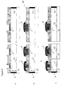
- This attachment process comprises the steps of (figure 4):
- an electroless bumping or plating bath is a liquid in which, on localised parts of an immersed substrate, conductive material present in this liquid is being deposited without external supply of charge carriers.
- the localised parts of the immersed substrate (1) are the metallic bonding pads (3) exposed to the liquid.
- the conductive material is a metal, e.g. nickel, copper.
- the pH range of such electroless plating bath is usually in the range from 2 to 12.
- the plating temperature of such plating baths is typically above 70 Celsius, normally about 90 °C.
- the bond pads connected to the ground/substrate will therefore be plated.
- This non-conductive carrier will avoid interference of the nickel deposition process.
- several chips or wafer parts can be attached to this non-conductive substrate and can be plated simultaneously.
- the individual dies can be removed from the carrier in a simple way. (see figure 4d) by causing an adhesive failure between the adhesive layer and the individual die.
- the chip can now be flip-chip bonded to an appropriate board.
- the process of plating single chips or wafer parts comprises the steps of:
- the removable carrier (15) used can be a commercially available film, e.g. from Nitto Corp. Japan, for example tape VD-8 or VD-15 (8 and 150 micron respectively), which is normally used as a temporary support in the process of the dicing wafers.
- the Nitto film is covered with a removable pressure-sensitive adhesive and will be described in the following as "Nitto tape”.
- Removable pressure sensitive adhesives which predictably adhere, yet remain peelable from a variety of substrates without damaging the substrate or leaving any adhesive residue on the surface, are described in the literature. They are often provided as a sheet material which may be unsupported or supported by a typically flexible backing such as, for example, polyester, biaxially-oriented polyethylene terephthalate film, pvc, or other suitable polymeric films.
- the removable pressure sensitive adhesive must provide a quick initial adhesion build-up (sufficient initial tack or quick stick) to quickly fix the adhesive to the desired substrate.
- the adhesive should exhibit only a low and at any rate an acceptable adhesion build-up with time, even at elevated temperatures, to ensure clean peelability after prolonged dwell times.
- the adhesive should furthermore be characterised by an adequate peel strength to give a reliable adhesion to the substrate without damaging on the other hand the substrate when removing the adhesive. On removal the adhesive should fail in adhesion to the semiconductor substrate - leaving a residue-free surface.
- the cohesive strength is adjusted to the thickness of the adhesive layer and must be the higher the thicker the adhesive layer in order to avoid cohesive failure on peeling off the tape.
- a sufficient cohesive strength is also required in order to limit the cold flow of the adhesive on a surface, a process which can lead to an undesirable building-up of peel strength over time.
- the static shear strength should be high enough to allow the light-duty mounting applications of the present invention without being too high to result in permanent adhesion.
- the cohesive strength, the shear strength and the peel adhesion are interrelated and they are mainly influenced by the cross-linking density, the loading with filler and the thickness of the adhesive layer.
- tapes are those made by Advanced Research Corp., USA, tapes ARclad® 7992, 8901, 8471 and those supplied by Permacel Corp. USA, e.g. P-377, P-366, P335 or P925.
- the wafer is attached to the Nitto tape, sawn into individual chips that can be individually removed from the tape by a vacuum pincet.
- Such films are not expected to withstand chemical processing as these tapes are only used in the mechanical process of dicing wafers.
- the single dice or chips are attached to a more rigid polyamide carrier, using an adhesive tape.
- This adhesive tape can be a commercial available tape as is being used when dicing wafers, such as the above mentioned Nitto-tape.
- This dicing tape used in our plating experiments, unexpectedly did not contaminate any of the different baths involved in electroless nickel plating and could withstand the process temperatures. After plating or bumping the chips were removed from the tape by using a vacuum pincet.
- Suitable removable pressure sensitive adhesives for use with the present invention should furthermore exhibit a high resistance to water and plating solutions.
- Figure 5 illustrates the preferred embodiment.
- Several dies (17) are attached to a Nitto tape (15) mounted in a rigid polyamide holder or frame (18).
- the handling of the dies is made very easy by using such holder.
- the holder will be put into the plating solutions.
- Figure 6 is a SEM picture showing the uniform plating resulting from the handling of the dies according to the present invention. All bond pads of the plated die (17) show substantially the same plating height.
- the bond pads (3a) in electrical connection with the substrate are white, while the insulated bond pads (3c) are dark as a result from the SEM operation.
- a second aspect of the invention is related to the type of carrier used.
- the carrier (15) supporting the die (17) must be at least as large as the bottom surface (11) of the die as illustrated in figure 7a.
- the step of attaching the die to an insulating substrate can be executed at wafer level.
- An insulating layer 15, 16 is then formed on or attached to the bottom surface and/or the side edges of the wafer before dicing the wafer.
- This layer 15,16 can be formed for example during a low-temperature Chemical Vapour Deposition process and can comprise non-conductive materials such as oxides or nitrides.
- This layer 15, 16 can be a resin layer.
- the stack of wafer and non-conductive substrate can be diced into individual dies or wafer parts, similar to the die shown in figure 5a.
- the wafer can be bonded to the carrier e.g. by glueing or other wafer-bonding techniques known in the art.
- This singulated die already has an electrically insulated bottom layer and can be attached to any type of carrier, insulating or non-insulating for subsequent plating.
- the type of carrier is limited to non-conductive carriers having a cure or melt temperature above 100°C or at least slightly above the process temperature of the plating bath, in order to avoid degradation of the carrier.
- This temperature limitation avoids contamination of the plating bath by dissolution of the carrier components, compounds or fractions thereof at elevated temperatures. It is known that plating baths, e.g. electroless nickel baths, are sensitive to contaminants.
- the carrier must remain intact or unaffected by the plating solution at the plating conditions, e.g. composition, pH or process temperature. The carrier must keep its integrity.
- the non-conductive substrate has a volume resistivity of at least 10 MOhm.cm and a surface resistivity of at least 1 Mohm.
- the substrate can be rigid or a flexible. Examples of suitable substrates are FR4, alumina substrates, glass substrates, Kapton flex, polyamide substrates, ceramic substrates, printed-board-circuit (PCB) substrates.
- a third aspect of the invention is related to attachment of the die to the carrier.
- the die is attached to the carrier preferably by a pressure-sensitive adhesive, preferably a removable pressure sensitive adhesive. Pressure sensitives adhesives or tapes are characterised in that in dry, i.e.
- Pressure sensitive adhesives are available in various grades of agressiveness, that is the peel strength which is achieved on application. They require no activation by water 'solvent" or heat to exert a strong adhesive holding force. They have a sufficiently cohesive holding force and elastic nature so that, despite their aggressive tackiness, they can be handled with the fingers and removed from smooth surfaces without leaving a residue. Removable pressure sensitive adhesives which predictably adhere, yet remain peelable from a variety of substrates without damaging the substrate or leaving any adhesive residue on the surface, are described in the literature.
- the removable pressure sensitive adhesive preferably provides a quick initial adhesion build-up (sufficient initial tack or quick stick) to quickly fix the adhesive to the desired substrate.
- the adhesive should exhibit only a low and at any rate acceptable adhesion build-up with time, even at elevated temperatures, to ensure clean peelability after prolonged dwell times.
- the adhesive should furthermore be characterised by an adequate peel strength to give a reliable adhesion to the substrate without damaging on the other hand the substrate when removing the adhesive.
- General trade usage by leading tape manufacturers does not sanction extension of the term "pressure sensitive" to embrace tapes and adhesives merely because they are sticky (e.g.' fly-papers)' or merely because they adhere or cohere to a particular type of surface (e.g. self-sealing envelopes).
- the cohesive strength is adjusted to the thickness of the adhesive layer and must be the higher the thicker the adhesive layer in order to avoid cohesive failure on peeling.
- a sufficient cohesive strength is also required in order to limit the cold flow of the adhesive on a surface, a process which can lead to an undesirable building-up of peel strength over time.
- the static shear strength should be high enough to allow the light-duty mounting applications of the present invention without being too high to result in permanent adhesion.
- the cohesive strength, the shear strength and the peel adhesion are interrelated and they are mainly influenced by the crosslinking density, the loading with filler and the thickness of the adhesive layer.
- the type of pressure-sensitive adhesives or glues is limited to those having a curing or melting temperature above 100°C or at least slightly above the process temperature of the plating bath.
- the process temperature of the plating bath must be below the temperature at which the pressure-sensitive adhesive looses its property of tackiness and ease of removal. Otherwise the adhesive might be cured or baked during the plating process. The thus cured adhesive would make detachment of the chip or wafer parts after plating impossible or only at the expense of residues left on the backside of the chip or wafer part.
- Adhesives having a curing or melting temperature below 100°C or below the process temperature of the plating bath could contaminate the plating bath.
- the chips or wafer parts are attached on a carrier by means of an insulating adhesive.
- This adhesive is preferably a pressure-sensitive adhesive.
- This insulating adhesive will electrically insulate the ground plane (7) or substrate (1) of the wafer part or die (17) from the plating bath (10).
- the insulating adhesive will at least cover the bottom surface of the die to avoid direct electrical contact between the carrier (15), which in this case can be conductive, and the chip (17) (see figure 5e).
- a disadvantage of this approach is that on the surfaces of a conductive carrier (15) parasitic plating can occur leading to an excess consumption of the plating metal.
- the present invention finds particular advantageous use when prototyping. In this case it is rare that a complete wafer is used for one type of semiconductor very large integrated circuit. To save costs, two or more designs are incorporated on one wafer. This means that each part of the wafer needs to be processed differently. This is done most easily by dicing the wafer and treating each die separately or in common groups. The plating process in accordance with the present invention can be used even with individual dies.
- the chips may be formed in a complete wafer and the back side of this wafer attached to a sheet coated with a removable pressure sensitive adhesive.
- the plating may be carried out on the wafer with the sheet attached or the wafer may be diced into wafer parts or dies with the sheet still attached and then the individual dies may be plated.
- the pressure sensitive sheet may be applied to parts of the wafer and these parts may then be plated with the sheet attached.
- an insulating layer 15 has been applied to the underside of a semiconductor substrate.
- This insulating layer 15 may be an insulating substrate to which the semiconductor substrate has been transferred or can be an insulating layer such as a resin layer or can be a tape with a removable pressure sensitive adhesive as defined above.
- the complete wafer is then plated in an electroless plating bath (figure 8b) to plate the bond pads 5. Subsequently, (figure 8c) the wafer is diced into individual dies or chips.
- the underside of the wafer may be attached to a tape with a removable pressure sensitive adhesive layer before plating and/or dicing and dicing carried out in such a way that the tame is left intact. Then each individual die can be removed from the tape one-by-one.
- Figure 9a starts from the same material as any of those described with reference to figure 8a.
- the wafer is diced as shown in figure 9b and then individual dies or chips are plated as shown in figure 9c.
- a tape with a removable pressure sensitive adhesive layer may be applied to the underside of the wafer before dicing. The dicing operation is carried out leaving the individual dies attached to the tape. Select ones of the dies may be removed or the tape may be cut into regions having several identical dies and/or dies for which the subsequent plating steps are the same.
- the bond pads 5 of the dies are then plated as described above. Subsequently they may be removed from the tape.
Landscapes
- Chemically Coating (AREA)
Abstract
Description
- cleaning of the aluminium (Al) alloy surface (3), thereby removing the native Al-oxide. This step is also called Al cleaner or Al microetch (figure 1a). Typically, a solution of NaOH is used to remove about 70nm of the aluminium surface to yield oxide free surfaces.
- rinsing in De Ionised water (DI-water) to remove excess chemicals.
- converting the Al surface into a zincate surface (4), by application of such a layer in a zincate bath (figure 1b). The Al layer is partially etched, during this step. The thus formed zinc layer prevents the Al surface from re-oxidation.
- rinsing in de-ionised water (DI-water), to avoid harmful zincate drag-in.
- electroless nickel deposition (5), by application in a nickel plating bath
- rinsing in DI-water
- immersion in a gold plating solution: coating a thin layer of gold (6) on the electroless deposited nickel surface (5).
- rinsing in DI-water
- providing an adhesive coated substrate, e.g. by the steps of:
- providing an insulating carrier or substrate (15) (figure 4a),
- applying a layer of an adhesive (16) onto this carrier (15) (figure 4b)
- attaching the single chips, wafer parts (17) or a wafer to this adhesive (16) (figure 4c).
A third aspect of the invention is related to attachment of the die to the carrier. The die is attached to the carrier preferably by a pressure-sensitive adhesive, preferably a removable pressure sensitive adhesive. Pressure sensitives adhesives or tapes are characterised in that in dry, i.e. solvent-free, form they are permanently tacky at room temperature and firmly adhere to a variety of dissimilar surfaces upon mere contact without the need of more than finger or hand pressure. Pressure sensitive adhesives are available in various grades of agressiveness, that is the peel strength which is achieved on application. They require no activation by water 'solvent" or heat to exert a strong adhesive holding force. They have a sufficiently cohesive holding force and elastic nature so that, despite their aggressive tackiness, they can be handled with the fingers and removed from smooth surfaces without leaving a residue. Removable pressure sensitive adhesives which predictably adhere, yet remain peelable from a variety of substrates without damaging the substrate or leaving any adhesive residue on the surface, are described in the literature. The removable pressure sensitive adhesive preferably provides a quick initial adhesion build-up (sufficient initial tack or quick stick) to quickly fix the adhesive to the desired substrate. On the other hand, the adhesive should exhibit only a low and at any rate acceptable adhesion build-up with time, even at elevated temperatures, to ensure clean peelability after prolonged dwell times. The adhesive should furthermore be characterised by an adequate peel strength to give a reliable adhesion to the substrate without damaging on the other hand the substrate when removing the adhesive. General trade usage by leading tape manufacturers does not sanction extension of the term "pressure sensitive" to embrace tapes and adhesives merely because they are sticky (e.g.' fly-papers)' or merely because they adhere or cohere to a particular type of surface (e.g. self-sealing envelopes).
Claims (15)
- A method for electroless plating semiconductor chips (17) comprising the steps ofattaching at least one semiconductor chip (17) having bonding pads to a carrier (15),electroless plating the bond pads (3) of the at least one semiconductor chip (17),detaching the at least one semiconductor chip from the carrier,wherein the step of attaching the at least one semiconductor chip to a carrier comprises the steps of:providing a carrier (15)), andattaching the at least one semiconductor chip (17) to the carrier using a pressuresensitive adhesive layer (16).
- A method as recited in claim 1, wherein the at least one semiconductor chip is an individual semiconductor chip.
- A method as recited in claim 1 or 2, wherein a plurality of semiconductor chips are attached to the carrier and plated simultaneously.
- A method as recited in any previous claim wherein said chip (17) is formed in or on a conductive substrate (1).
- A method as recited in any of the previous claims, wherein said pressure sensitive adhesive is a non-conducting adhesive.
- A method as recited in any previous claim wherein said pressure-sensitive adhesive remains operable above a maximum temperature used in the plating process.
- A method as recited in claim 6 wherein the pressure-sensitive adhesive remains operable above 100 °C.
- A method as recited in any previous claim wherein said carrier is a non-conductive carrier.
- A method as recited in claim 8 wherein said carrier has a volume resistivity of at least 10 MOhm.cm and a surface resistivity of at least 1 Mohm.
- A method as recited in any previous claim, wherein said carrier keeps its mechanical integrity at temperatures above 100 Celsius.
- A method as recited in claim 10 wherein said carrier is selected from the group of FR-substrates, glass substrate, PCB substrates, polyamide substrates, ceramic substrates.
- A method as recited in any previous claim wherein said electroless plating process is an electroless nickel plating process.
- A devices obtained by the use of any of the methods in claims 1 to 12.
- A method for electroless plating individual semiconductor chips (17) with bonding pads comprising the steps of:attaching the individual semiconductor chip to a carrier (15),electroless plating the bond pads (3) of said individual semiconductor chip (17),detaching the individual semiconductor chip from the carrier,wherein said step of attaching the individual semiconductor chip to the carrier comprises the steps of:forming a semiconductor wafer having two major surfaces with bonding pads on one major surface,forming an insulating layer at least on the other major surface of the wafer,dicing the semiconductor wafer into individual chips.
- A method as recited in claim 14 wherein said step of forming an insulating layer at least on the other major surface of the semiconductor wafer comprises the step of attaching the wafer to a non-conductive carrier using a pressure-sensitive adhesive.
Applications Claiming Priority (2)
| Application Number | Priority Date | Filing Date | Title |
|---|---|---|---|
| US19942100P | 2000-04-24 | 2000-04-24 | |
| US199421P | 2000-04-24 |
Publications (2)
| Publication Number | Publication Date |
|---|---|
| EP1156521A2 true EP1156521A2 (en) | 2001-11-21 |
| EP1156521A3 EP1156521A3 (en) | 2007-05-23 |
Family
ID=22737419
Family Applications (1)
| Application Number | Title | Priority Date | Filing Date |
|---|---|---|---|
| EP01870087A Ceased EP1156521A3 (en) | 2000-04-24 | 2001-04-24 | Low cost electroless plating process for single chips and wafer parts and products obtained thereof |
Country Status (2)
| Country | Link |
|---|---|
| US (1) | US6548327B2 (en) |
| EP (1) | EP1156521A3 (en) |
Families Citing this family (26)
| Publication number | Priority date | Publication date | Assignee | Title |
|---|---|---|---|---|
| DE10103294C1 (en) * | 2001-01-25 | 2002-10-31 | Siemens Ag | Carrier with a metal surface and at least one chip arranged thereon, in particular power semiconductors |
| KR100476301B1 (en) * | 2002-07-27 | 2005-03-15 | 한국과학기술원 | Fabrication Method of multilayer UBM by Electroplating for Flip chip Interconnections |
| US20040036171A1 (en) * | 2002-08-22 | 2004-02-26 | Farnworth Warren M. | Method and apparatus for enabling a stitch wire bond in the absence of discrete bump formation, semiconductor device assemblies and electronic systems including same |
| JP4107417B2 (en) * | 2002-10-15 | 2008-06-25 | 日東電工株式会社 | Tip workpiece fixing method |
| JP4283596B2 (en) * | 2003-05-29 | 2009-06-24 | 日東電工株式会社 | Tip workpiece fixing method |
| US7081372B2 (en) * | 2003-07-09 | 2006-07-25 | Chartered Semiconductor Manufacturing Ltd. | Aluminum cap with electroless nickel/immersion gold |
| US7294565B2 (en) * | 2003-10-01 | 2007-11-13 | International Business Machines Corporation | Method of fabricating a wire bond pad with Ni/Au metallization |
| US6936524B2 (en) * | 2003-11-05 | 2005-08-30 | Akustica, Inc. | Ultrathin form factor MEMS microphones and microspeakers |
| JP4275522B2 (en) * | 2003-12-26 | 2009-06-10 | 日東電工株式会社 | Dicing die bond film |
| JP4443962B2 (en) * | 2004-03-17 | 2010-03-31 | 日東電工株式会社 | Dicing die bond film |
| US7151010B2 (en) * | 2004-12-01 | 2006-12-19 | Kyocera Wireless Corp. | Methods for assembling a stack package for high density integrated circuits |
| US7217994B2 (en) * | 2004-12-01 | 2007-05-15 | Kyocera Wireless Corp. | Stack package for high density integrated circuits |
| US7700911B1 (en) * | 2005-03-04 | 2010-04-20 | University Of South Florida | Fabrication of 3-D ion optics assemblies by metallization of non-conductive substrates |
| US7807505B2 (en) * | 2005-08-30 | 2010-10-05 | Micron Technology, Inc. | Methods for wafer-level packaging of microfeature devices and microfeature devices formed using such methods |
| JP4728828B2 (en) * | 2006-02-09 | 2011-07-20 | パナソニック株式会社 | Wiring board manufacturing method |
| KR100943799B1 (en) * | 2006-09-12 | 2010-02-23 | 닛토덴코 가부시키가이샤 | Dicing die bond film |
| US20100142167A1 (en) * | 2006-11-24 | 2010-06-10 | Fraunhofer-Gesellschaft Zur Forderung Der Angewandten Forschung E.V. | Electronic, in particular microelectronic, functional group and method for its production |
| KR100850212B1 (en) * | 2007-04-20 | 2008-08-04 | 삼성전자주식회사 | Manufacturing Method of Semiconductor Device to Obtain Uniform Electroless Plating Thickness |
| US8609256B2 (en) | 2008-10-02 | 2013-12-17 | E I Du Pont De Nemours And Company | Nickel-gold plateable thick film silver paste |
| CN102034721B (en) | 2010-11-05 | 2013-07-10 | 南通富士通微电子股份有限公司 | Method for encapsulating chip |
| CN102034720B (en) * | 2010-11-05 | 2013-05-15 | 南通富士通微电子股份有限公司 | Chip packaging method |
| US20130299947A1 (en) * | 2012-05-14 | 2013-11-14 | Freescale Semiconductor, Inc. | Passivated test structures to enable saw singulation of wafer |
| CN108367822A (en) * | 2015-09-21 | 2018-08-03 | 弗莱沃塞尔公司 | coating packaging product, system and method |
| CN105460888A (en) * | 2015-11-19 | 2016-04-06 | 博奥生物集团有限公司 | Chip packaging method |
| CN110769944B (en) * | 2017-02-03 | 2022-03-25 | 印可得株式会社 | Electromagnetic wave shielding coating method |
| KR102044773B1 (en) * | 2017-02-03 | 2019-11-18 | (주)잉크테크 | electromagnetic wave shield coating method |
Family Cites Families (7)
| Publication number | Priority date | Publication date | Assignee | Title |
|---|---|---|---|---|
| JP2682250B2 (en) * | 1991-03-20 | 1997-11-26 | 株式会社村田製作所 | Electronic component chip holder and electronic component chip handling method |
| US5171712A (en) * | 1991-12-20 | 1992-12-15 | Vlsi Technology, Inc. | Method of constructing termination electrodes on yielded semiconductor die by visibly aligning the die pads through a transparent substrate |
| US5872051A (en) * | 1995-08-02 | 1999-02-16 | International Business Machines Corporation | Process for transferring material to semiconductor chip conductive pads using a transfer substrate |
| US5789278A (en) * | 1996-07-30 | 1998-08-04 | Micron Technology, Inc. | Method for fabricating chip modules |
| JP3955659B2 (en) * | 1997-06-12 | 2007-08-08 | リンテック株式会社 | Electronic component die bonding method and die bonding apparatus used therefor |
| TW396462B (en) * | 1998-12-17 | 2000-07-01 | Eriston Technologies Pte Ltd | Bumpless flip chip assembly with solder via |
| US6329228B1 (en) * | 1999-04-28 | 2001-12-11 | Citizen Watch Co., Ltd. | Semiconductor device and method of fabricating the same |
-
2001
- 2001-04-24 US US09/841,359 patent/US6548327B2/en not_active Expired - Lifetime
- 2001-04-24 EP EP01870087A patent/EP1156521A3/en not_active Ceased
Also Published As
| Publication number | Publication date |
|---|---|
| US6548327B2 (en) | 2003-04-15 |
| US20020001670A1 (en) | 2002-01-03 |
| EP1156521A3 (en) | 2007-05-23 |
Similar Documents
| Publication | Publication Date | Title |
|---|---|---|
| US6548327B2 (en) | Low cost electroless plating process for single chips and wafer parts and products obtained thereof | |
| KR101080629B1 (en) | Electroless and immersion plating of integrated circuits using an activation plate | |
| US7498240B2 (en) | Microfeature workpieces, carriers, and associated methods | |
| US8329554B2 (en) | Ultra thin bumped wafer with under-film | |
| KR20040086831A (en) | Manufacturing method of semiconductor device | |
| US9613932B2 (en) | Integrated circuit package and method of making same | |
| JPH09199506A (en) | Bump forming method for semiconductor element | |
| US6405429B1 (en) | Microbeam assembly and associated method for integrated circuit interconnection to substrates | |
| KR100592121B1 (en) | No-clean flux for flip chip assembly | |
| WO1993013550A1 (en) | A method of constructing termination electrodes on yielded semiconductor die | |
| KR20080110813A (en) | Gaas integrated circuit device and method of attaching same | |
| US7067423B2 (en) | Electroless plating apparatus, semiconductor wafer having bumps, semiconductor chip having bumps, methods of manufacturing the semiconductor wafer and the semiconductor chip, semiconductor device, circuit board, and electronic equipment | |
| JP3114926B2 (en) | Masking method for wiring board plating | |
| CN120981910A (en) | Copper pad metallization system and related methods | |
| JP2004063516A (en) | Method for manufacturing semiconductor device | |
| JP2000299339A (en) | Method for manufacturing semiconductor device | |
| US7476606B2 (en) | Eutectic bonding of ultrathin semiconductors | |
| CN114937615A (en) | Method for realizing packaging structure of ultrathin wafer level wafer | |
| US20250279377A1 (en) | Copper pad interconnect systems and related methods | |
| CN115172146B (en) | Methods for fabricating compound semiconductor wafers | |
| EP3692572A1 (en) | Structure and method for semiconductor packaging | |
| JPH09116251A (en) | Semiconductor bare chip mounting method and mounting structure | |
| JP2002026218A (en) | Manufacturing method of wiring board | |
| JPS6086840A (en) | Manufacture of semiconductor device | |
| JP2003007913A (en) | Semiconductor device and method of manufacturing semiconductor module |
Legal Events
| Date | Code | Title | Description |
|---|---|---|---|
| PUAI | Public reference made under article 153(3) epc to a published international application that has entered the european phase |
Free format text: ORIGINAL CODE: 0009012 |
|
| AK | Designated contracting states |
Kind code of ref document: A2 Designated state(s): AT BE CH CY DE DK ES FI FR GB GR IE IT LI LU MC NL PT SE TR |
|
| AX | Request for extension of the european patent |
Free format text: AL;LT;LV;MK;RO;SI |
|
| PUAL | Search report despatched |
Free format text: ORIGINAL CODE: 0009013 |
|
| AK | Designated contracting states |
Kind code of ref document: A3 Designated state(s): AT BE CH CY DE DK ES FI FR GB GR IE IT LI LU MC NL PT SE TR |
|
| AX | Request for extension of the european patent |
Extension state: AL LT LV MK RO SI |
|
| 17P | Request for examination filed |
Effective date: 20071106 |
|
| AKX | Designation fees paid |
Designated state(s): AT BE CH CY DE DK ES FI FR GB GR IE IT LI LU MC NL PT SE TR |
|
| 17Q | First examination report despatched |
Effective date: 20080118 |
|
| RAP1 | Party data changed (applicant data changed or rights of an application transferred) |
Owner name: UNIVERSITEIT GENT Owner name: IMEC |
|
| STAA | Information on the status of an ep patent application or granted ep patent |
Free format text: STATUS: THE APPLICATION HAS BEEN REFUSED |
|
| 18R | Application refused |
Effective date: 20110510 |