EP1156138A2 - Electrode material for forming stamper and thin film for forming stamper - Google Patents
Electrode material for forming stamper and thin film for forming stamper Download PDFInfo
- Publication number
- EP1156138A2 EP1156138A2 EP01111581A EP01111581A EP1156138A2 EP 1156138 A2 EP1156138 A2 EP 1156138A2 EP 01111581 A EP01111581 A EP 01111581A EP 01111581 A EP01111581 A EP 01111581A EP 1156138 A2 EP1156138 A2 EP 1156138A2
- Authority
- EP
- European Patent Office
- Prior art keywords
- stamper
- thin film
- electrode
- forming
- electrocasting
- Prior art date
- Legal status (The legal status is an assumption and is not a legal conclusion. Google has not performed a legal analysis and makes no representation as to the accuracy of the status listed.)
- Withdrawn
Links
Images



Classifications
-
- G—PHYSICS
- G11—INFORMATION STORAGE
- G11B—INFORMATION STORAGE BASED ON RELATIVE MOVEMENT BETWEEN RECORD CARRIER AND TRANSDUCER
- G11B7/00—Recording or reproducing by optical means, e.g. recording using a thermal beam of optical radiation by modifying optical properties or the physical structure, reproducing using an optical beam at lower power by sensing optical properties; Record carriers therefor
- G11B7/24—Record carriers characterised by shape, structure or physical properties, or by the selection of the material
- G11B7/26—Apparatus or processes specially adapted for the manufacture of record carriers
- G11B7/263—Preparing and using a stamper, e.g. pressing or injection molding substrates
-
- C—CHEMISTRY; METALLURGY
- C25—ELECTROLYTIC OR ELECTROPHORETIC PROCESSES; APPARATUS THEREFOR
- C25D—PROCESSES FOR THE ELECTROLYTIC OR ELECTROPHORETIC PRODUCTION OF COATINGS; ELECTROFORMING; APPARATUS THEREFOR
- C25D1/00—Electroforming
- C25D1/10—Moulds; Masks; Masterforms
-
- G—PHYSICS
- G11—INFORMATION STORAGE
- G11B—INFORMATION STORAGE BASED ON RELATIVE MOVEMENT BETWEEN RECORD CARRIER AND TRANSDUCER
- G11B2220/00—Record carriers by type
- G11B2220/20—Disc-shaped record carriers
- G11B2220/25—Disc-shaped record carriers characterised in that the disc is based on a specific recording technology
- G11B2220/2537—Optical discs
-
- Y—GENERAL TAGGING OF NEW TECHNOLOGICAL DEVELOPMENTS; GENERAL TAGGING OF CROSS-SECTIONAL TECHNOLOGIES SPANNING OVER SEVERAL SECTIONS OF THE IPC; TECHNICAL SUBJECTS COVERED BY FORMER USPC CROSS-REFERENCE ART COLLECTIONS [XRACs] AND DIGESTS
- Y10—TECHNICAL SUBJECTS COVERED BY FORMER USPC
- Y10T—TECHNICAL SUBJECTS COVERED BY FORMER US CLASSIFICATION
- Y10T428/00—Stock material or miscellaneous articles
- Y10T428/12—All metal or with adjacent metals
- Y10T428/12493—Composite; i.e., plural, adjacent, spatially distinct metal components [e.g., layers, joint, etc.]
- Y10T428/12535—Composite; i.e., plural, adjacent, spatially distinct metal components [e.g., layers, joint, etc.] with additional, spatially distinct nonmetal component
- Y10T428/12597—Noncrystalline silica or noncrystalline plural-oxide component [e.g., glass, etc.]
-
- Y—GENERAL TAGGING OF NEW TECHNOLOGICAL DEVELOPMENTS; GENERAL TAGGING OF CROSS-SECTIONAL TECHNOLOGIES SPANNING OVER SEVERAL SECTIONS OF THE IPC; TECHNICAL SUBJECTS COVERED BY FORMER USPC CROSS-REFERENCE ART COLLECTIONS [XRACs] AND DIGESTS
- Y10—TECHNICAL SUBJECTS COVERED BY FORMER USPC
- Y10T—TECHNICAL SUBJECTS COVERED BY FORMER US CLASSIFICATION
- Y10T428/00—Stock material or miscellaneous articles
- Y10T428/12—All metal or with adjacent metals
- Y10T428/12493—Composite; i.e., plural, adjacent, spatially distinct metal components [e.g., layers, joint, etc.]
- Y10T428/12771—Transition metal-base component
- Y10T428/12861—Group VIII or IB metal-base component
- Y10T428/12944—Ni-base component
Definitions
- the present invention relates to a thin film for forming stamper used as an electrode formed on the surface of a patterned resist material for electrocasting a stamper material, and an electrode material for forming stamper used as the material of such an electrode.
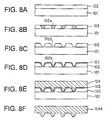
- FIG. 8 shows a conventional stamper manufacturing method.
- a photoresist film 102 is formed on a glass substrate 101 by spin coating or other process, and then, as shown in FIG. 8B, the photoresist film 102 is exposed by laser beam and a latent image 102a is formed.
- the photoresist film 102 is developed, and a pattern having a groove 102b as shown in FIG. 8C is formed.
- a nickel thin film 103 is formed on the surface of the photoresist film 102 and glass substrate 101 by sputtering, vapor deposition or other method.
- nickel electrocasting is applied on the surface of the nickel thin film 103, and a nickel layer 104 is formed.
- the nickel layer 104 is separated from the glass substrate 101, and, for example, the top surface of the nickel layer 104 in FIG. 8F is polished, and a stamper 104A is obtained.
- a further higher recording density is required in optical disks.
- the conventional laser beam cutting using laser beam is not applicable, and electron beam cutting using electron beam is noticed as a method replacing the laser beam cutting.
- the electron beam cutting as compared with the conventional laser beam cutting, a pattern of higher definition can be formed.
- the electron absorption sensitivity of the resist material must be improved, and an electron-attracting radical such as chlorine, sulfur or fluorine is added to the resist material.
- an electron-attracting radical such as chlorine, sulfur or fluorine is added to the resist material.
- the electron-attracting radical in the resist material and the nickel thin film react with each other, and the nickel thin film is damaged, and the quality of the stamper deteriorates.
- the electrode material for forming stamper of the invention is an electrode material for forming stamper used as a material of an electrode formed on the surface of a patterned resist material for electrocasting a stamper material, in which Ni element is a principal component, and Ru element is added in a range of less than 25 percent by weight.
- this electrode material for forming stamper since reaction between Ni in the electrode material and the electron-attracting radical contained in the resist material is suppressed, deterioration of stamper quality can be prevented. Further, the electrode excellent in flatness is formed, so that the S/N ratio of the optical disk may be enhanced.
- the electrode material for forming stamper of the invention is an electrode material for forming stamper used as a material of an electrode formed on the surface of a patterned resist material for electrocasting a stamper material, in which Ni element is a principal component, and Cu element is added in a range of less than 25 percent by weight.
- the electrode material for forming stamper of the invention is an electrode material for forming stamper used as a material of an electrode formed on the surface of a patterned resist material for electrocasting a stamper material, in which Ni element is a principal component, and P element is added in a range of less than 25 percent by weight.
- the electrode material for forming stamper of the invention is an electrode material for forming stamper used as a material of an electrode formed on the surface of a patterned resist material for electrocasting a stamper material, in which Ni element is a principal component, and Mg element is added in a range of less than 25 percent by weight.
- the electrode material for forming stamper of the invention is an electrode material for forming stamper used as a material of an electrode formed on the surface of a patterned resist material for electrocasting a stamper material, in which Ni element is a principal component, and Cr element is added in a range of less than 25 percent by weight.
- this electrode material for forming stamper since reaction between Ni in the electrode material and the electron-attracting radical contained in the resist material is suppressed, deterioration of stamper quality can be prevented. Further, the electrode excellent in flatness is formed, so that the S/N ratio of the optical disk may be enhanced.
- the electrode material for forming stamper of the invention is an electrode material for forming stamper used as a material of an electrode formed on the surface of a patterned resist material for electrocasting a stamper material, in which Ni element is a principal component, and Au element is added in a range of less than 25 percent by weight.
- the electrode material for forming stamper of the invention is an electrode material for forming stamper used as a material of an electrode formed on the surface of a patterned resist material for electrocasting a stamper material, in which Ni element is a principal component, and Si element is added in a range of less than 25 percent by weight.
- the electrode material for forming stamper of the invention is an electrode material for forming stamper used as a material of an electrode formed on the surface of a patterned resist material for electrocasting a stamper material, in which Ni element is a principal component, and Ti element is added in a range of less than 50 percent by weight.
- the material for forming stamper of the invention is an electrode material for forming stamper used as a material of an electrode formed on the surface of a patterned resist material for electrocasting a stamper material, in which Ni element is a principal component, and Ag element is added in a range of less than 50 percent by weight.
- this electrode material for forming stamper since reaction between Ni in the electrode material and the electron-attracting radical contained in the resist material is suppressed, deterioration of stamper quality can be prevented. Further, the electrode excellent in flatness is formed, so that the S/N ratio of the optical disk may be enhanced.
- the thin film for forming stamper of the invention is a thin film for forming stamper used as an electrode formed on the surface of a patterned resist material for electrocasting a stamper material, in which Ni element is a principal component, and Ru element is added in a range of less than 25 percent by weight.
- the thin film for forming stamper of the invention is a thin film for forming stamper used as an electrode formed on the surface of a patterned resist material for electrocasting a stamper material, in which Ni element is a principal component, and Cu element is added in a range of less than 25 percent by weight.
- the thin film for forming stamper of the invention is a thin film for forming stamper used as an electrode formed on the surface of a patterned resist material for electrocasting a stamper material, in which Ni element is a principal component, and P element is added in a range of less than 25 percent by weight,
- the thin film for forming stamper of the invention is a thin film for forming stamper used as an electrode formed on the surface of a patterned resist material for electrocasting a stamper material, in which Ni element is a principal component, and Mg element is added in a range of less than 25 percent by weight.
- the thin film for forming stamper of the invention is a thin film for forming stamper used as an electrode formed on the surface of a patterned resist material for electrocasting a stamper material, in which Ni element is a principal component, and Cr element is added in a range of less than 25 percent by weight.
- the thin film for forming stamper of the invention is a thin film for forming stamper used as an electrode formed on the surface of a patterned resist material for electrocasting a stamper material, in which Ni element is a principal component, and Au element is added in a range of less than 25 percent by weight.
- the thin film for forming stamper of the invention is a thin film for forming stamper used as an electrode formed on the surface of a patterned resist material for electrocasting a stamper material, in which Ni element is a principal component, and Si element is added in a range of less than 25 percent by weight.
- the thin film for forming stamper of the invention is a thin film for forming stamper used as an electrode formed on the surface of a patterned resist material for electrocasting a stamper material, in which Ni element is a principal component, and Ti element is added in a range of less than 50 percent by weight.
- the thin film for forming stamper of the invention is a thin film for forming stamper used as an electrode formed on the surface of a patterned resist material for electrocasting a stamper material, in which Ni element is a principal component, and Ag element is added in a range of less than 50 percent by weight.
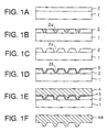
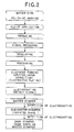
- FIGs. 1A to 1F are sectional views showing a process of manufacturing a stamper for manufacturing an optical disk by using a thin film for forming the stamper of the embodiment, and FIG. 2 shows the detail of the process.
- a glass substrate 1 is polished and washed, and an electron beam resist film 2 for electron beam is formed on the glass substrate 1 by spin coating or other method.
- the electron beam resist film 2 is prebaked, and the electron beam resist film 2 is exposed by an electron beam as shown in FIG. 1B, so that a latent image 2a is formed ("signal recording" in FIG. 2).
- the electron beam resist film 2 is developed, a groove 2b as shown in FIG. 1C is formed, and the electron beam resist film 2 is postbaked.
- a nickel alloy thin film 3 is formed on the surface of the electron beam resist film 2 and glass substrate 1 by sputtering, vapor deposition, or electroless plating.
- the material of the nickel alloy thin film is described later.
- nickel electrocasting is applied on the surface of the nickel alloy thin film 3, and a nickel layer 4 is formed.
- the nickel layer 4 is separated from the glass substrate 1, and, for example, the top surface of the nickel layer 4 in FIG. 1F is polished, and a master stamper 4A is obtained.
- a nickel alloy layer may be formed by electrocasting, and the separated nickel alloy layer may be used as stamper.
- FIG. 3 shows a process of manufacturing an optical disk by using a master stamper 4A or baby stamper. As shown in FIG. 3, after injection molding by using the stamper, a reflective film and a protective film are formed, and an optical disk is manufactured. The process in FIG. 3 is same as an ordinary manufacturing process, and detailed description is omitted.
- the material of the nickel alloy thin film 3 is a nickel alloy comprising Ni element as a principal component, and at least one of elements Ru, Cu, P, Mg, Cr, Au, Si, Ti, and Ag added in a range of less than 50 percent by weight.
- Ni element as a principal component
- at least one of elements Ru, Cu, P, Mg, Cr, Au, Si, Ti, and Ag added in a range of less than 50 percent by weight.
- the elements P, Mg, Si are added, and when the content of these elements is less than 25 percent by weight, these elements do not react with the principal component of Ni unless heated at least to about 400 to 500°C. Accordingly, in a thin film state, P, Mg, or Si deposits on the grain boundary of Ni, and is bonded with oxygen to be oxidized in other environment than inert atmosphere. In this case, in a state of an alloy thin film mainly composed of Ni, the oxide film of the added P, Mg, or Si deposits not only on the Ni grain boundary, but also on the thin film surface.
- the surface oxide film depositing on the thin film surface becomes a non-conductor to act as a barrier material for reaction between incoming active metal or non-metallic element and Ni, and it has been confirmed that the weather resistance of the Ni alloy is enhanced.
- the additive element such as P, Mg, or Si is likely to be bonded with oxygen, and also with other active non-metallic element, and therefore if added in excess, the weather resistance is lowered to the contrary. It hence seems to be proper by adding in a range of less than 25 percent by weight.
- Ni when adding Ti to the principal component Ni, except when also forming a compound by reaction while heating in high temperature atmosphere, Ti deposits on the Ni grain boundary.
- Such Ni alloy with Ti does not form non-conductor, but since Ti is stable in chlorine, it is effective to suppress exudation of active element into Ni grains or chemical reaction, and it seems to prevent chemical reaction on Ni grains.
- a solid solution is formed at a specific content, at least at less than 10 percent by weight, and a same solid solution as when adding Cu or Au has been confirmed.
- Ru, Ag, or Cr is added by more than 10 percent by weight, exceeding the solid solution limit, the whole added content is not dissolved, but Ru, Ag, or Cr deposits on the grain boundary of solid solution.
- the resistance to chlorination is enhanced as compared with that of pure Ni.
- the alloy thin film of Ni with at least one of Ru. Ag, and Cr is not only improved in chlorination resistance, but also enhanced in flatness of thin film.
- the flatness of thin film has been confirmed in the signal characteristic in reproduction of an optical disk manufactured by using the stamper formed by using this alloy thin film.
- Ru, Ag, or Cr is solidified to form a solid solution, it has been confirmed that the crystal structure of the principal component Ni is distorted to micronize thin film particles.
- the non-solidified additive content of the additive element existing in the grain boundary may be considered to be effective to promote stress relaxation.
- compositions of nickel alloy described in the embodiment are excellent in ductility and processability same as pure Ni, and also have chlorination resistance and bromination resistance, and are hence applicable to uses and application technologies hitherto limited because of the nature of pure Ni likely to react with chlorine or bromine.
- Ni and sputtering targets of additive metals Ru, Cu, P, Mg, Cr, Au, Si, Ti, and Ag the sputtering target of specified element and Ni were put in an RF magnetron sputtering apparatus, and a thin film was formed on a quartz substrate.
- the sputtering target was 3 inches (7.62 cm) in diameter, and 5 mm in thickness, and the distance from the sputtering target to the substrate was about 90 mm. While controlling the discharge amount of metal atoms by RF feed power to Ni and sputtering target of specified element, two metals were stacked up on the substrate simultaneously.
- the final degree of vacuum is 3 x 10 -5 Pa and the gas pressure when forming film is 0.7 to 1 Pa.
- the RF feed power was varied in a range of 100 to 500 W depending on the composition of the alloy.
- thin films of Ni-Ru alloy, Ni-Cu alloy, Ni-P alloy, Ni-Mg alloy, Ni-Cr alloy, Ni-Au alloy, Ni-Si alloy, Ni-Ti alloy, and Ni-Ag alloy were formed on substrates.
- the content of Ru, Cu, P, Mg, Cr, Au. Si, Ti, and Ag was varied in five concentrations, 1, 5, 10, 20, and 25 percent by weight.
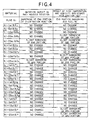
- a pure Ni thin film was formed on the substrate by using the same apparatus (see FIG. 4 and FIG. 5).
- the quartz substrates having the thin films stacked up thereon by the above method were immersed in sodium chloride aqueous solution and let stand for a specified time, and observed changes with time are shown in FIG. 4 and FIG. 5.
- the sodium chloride contained in the sodium chloride aqueous solution is 5 percent by volume, and the quartz substrates were immersed in the aqueous solution for about 96 hours at ordinary temperature without heating, After standing for 96 hours, changes with time of the thin film were visually observed, and the optical characteristics such as reflectivity of thin film were inspected by spectrophotometer, and changes of surface state of thin films were evaluated.
- Ni-Ru alloy Ni-Cu alloy, Ni-P alloy, Ni-Mg alloy, Ni-Cr alloy, Ni-Au alloy, Ni-Si alloy, Ni-Ti alloy, and Ni-Ag alloy
- Ni-25 wt.% Ru Ni-25 wt.% Cu, Ni-25 wt.% Mg, Ni-25 wt.% Cr, Ni-25 wt.% Au, and Ni-25 wt.% Si
- Ni-25 wt.% Ru, Ni-25 wt.% Cu, Ni-25 wt.% Mg, Ni-25 wt.% Cr, Ni-25 wt.% Au, and Ni-25 wt.% Si as a result of immersion in sodium chloride aqueous solution, a slight darkening in the end portion was noted. No change was observed in other alloy thin films.
- Ni-20 wt.% Ru, Ni-25 wt.% Ru, Ni-20 wt.% Cu, Ni-25 wt.% Cu, Ni-20 wt.% P, Ni-25 wt.% P, Ni-25 wt.% Cr, and Ni-25 wt.% Si as a result of high temperature and humidity resistance acceleration test, a slight darkening in the end portion was noted.
- FIG. 6 is a diagram showing a disk noise measuring method by a mirror section reproduced signal of an optical disk
- FIG. 7 is a diagram showing results of measurement.
- a resist layer 12 is formed on a glass substrate 11, and thin films 13 of pure Ni and Ni-5 wt.% Ru are formed thereon as electrode materials, and mother disks for measurement were prepared.
- the mother disk for measurement was rotated at linear velocity of 3 m/s and irradiated with light beam through a lens 14 from the side of the glass substrate 11, and the reflected light from the interface of the resist layer 12 and thin film 13 was received.
- the level of 1 MHz component was measured as noise component, and the result is shown in FIG. 7.
- the disk noise is -74.3 dB in the case of using pure Ni as the material for the thin film 13
- the disk noise is -79.7 dB in the case of using Ni-5 wt.% Ru as the material for the thin film 13. Therefore, in the case of Ni-5 wt.% Ru, the S/N ratio is improved by more than 5 dB as compared with the case of pure Ni. This result suggests that the flatness of the thin film of Ni-5 wt.% RU is superior to that of pure Ni, showing excellent suitability as the material used in manufacture of optical mother disk.
Landscapes
- Chemical & Material Sciences (AREA)
- Engineering & Computer Science (AREA)
- Chemical Kinetics & Catalysis (AREA)
- Electrochemistry (AREA)
- Materials Engineering (AREA)
- Metallurgy (AREA)
- Organic Chemistry (AREA)
- Manufacturing & Machinery (AREA)
- Manufacturing Optical Record Carriers (AREA)
- Moulds For Moulding Plastics Or The Like (AREA)
- Physical Vapour Deposition (AREA)
Abstract
Description
Claims (18)
- An electrode material for forming stamper used as a material of an electrode(3) formed on the surface of a patterned resisit material(2) for electrocasting a stamper material,
wherein Ni element is a principal component, and Ru element is added in a range of less than 25 percent by weight. - An electrode material for forming stamper used as a material of an electrode(3) formed on the surface of a patterned resisit material(2) for electrocasting a stamper material,
wherein Ni element is a principal component, and Cu element is added in a range of less than 25 percent by weight. - An electrode material for forming stamper used as a material of an electrode(3) formed on the surface of a patterned resisit material(2) for electrocasting a stamper material,
wherein Ni element is a principal component, and P element is added in a range of less than 25 percent by weight. - An electrode material for forming stamper used as a material of an electrode(3) formed on the surface of a patterned resisit material(2) for electrocasting a stamper material,
wherein Ni element is a principal component, and Mg element is added in a range of less than 25 percent by weight. - An electrode material for forming stamper used as a material of an electrode(3) formed on the surface of a patterned resisit material(2) for electrocasting a stamper material,
wherein Ni element is a principal component, and Cr element is added in a range of less than 25 percent by weight. - An electrode material for forming stamper used as a material of an electrode(3) formed on the surface of a patterned resisit material(2) for electrocasting a stamper material,
wherein Ni element is a principal component, and Au element is added in a range of less than 25 percent by weight. - An electrode material for forming stamper used as a material of an electrode(3) formed on the surface of a patterned resisit material(2) for electrocasting a stamper material,
wherein Ni element is a principal component, and Si element is added in a range of less than 25 percent by weight. - An electrode material for forming stamper used as a material of an electrode(3) formed on the surface of a patterned resisit material(2) for electrocasting a stamper material,
wherein Ni element is a principal component, and Ti element is added in a range of less than 50 percent by weight. - An electrode material for forming stamper used as a material of an electrode(3) formed on the surface of a patterned resisit material(2) for electrocasting a stamper material.
wherein Ni element is a principal component, and Ag element is added in a range of less than 50 percent by weight. - A thin film for forming stamper used as an electrode(3) formed on the surface of a patterned resisit material(2) for electrocasting a stamper material,
wherein Ni element is a principal component, and Ru element is added in a range of less than 25 percent by weight. - A thin film for forming stamper used as an electrode(3) formed on the surface of a patterned resisit material(2) for electrocasting a stamper material.
wherein Ni element is a principal component, and Cu element is added in a range of less than 25 percent by weight. - A thin film for forming stamper used as an electrode(3) formed on the surface of a patterned resisit material(2) for electrocasting a stamper material,
wherein Ni element is a principal component, and P element is added in a range of less than 25 percent by weight. - A thin film for forming stamper used as an electrode(3) formed on the surface of a patterned resisit material(2) for electrocasting a stamper material,
wherein Ni element is a principal component, and Mg element is added in a range of less than 25 percent by weight. - A thin film for forming stamper used as an electrode(3) formed on the surface of a patterned resisit material(2) for electrocasting a stamper material,
wherein Ni element is a principal component, and Cr element is added in a range of less than 25 percent by weight. - A thin film for forming stamper used as an electrode(3) formed on the surface of a patterned resisit material(2) for electrocasting a stamper material,
wherein Ni element is a principal component, and Au element is added in a range of less than 25 percent by weight. - A thin film for forming stamper used as an electrode(3) formed on the surface of a patterned resisit material(2) for electrocasting a stamper material,
wherein Ni element is a principal component, and Si element is added in a range of less than 25 percent by weight. - A thin film for forming stamper used as an electrode(3) formed on the surface of a patterned resisit material(2) for electrocasting a stamper material.
wherein Ni element is a principal component, and Ti element is added in a range of less than 50 percent by weight. - A thin film for forming stamper used as an electrode(3) formed on the surface of a patterned resisit material(2) for electrocasting a stamper material,
wherein Ni element is a principal component, and Ag element is added in a range of less than 50 percent by weight.
Applications Claiming Priority (2)
| Application Number | Priority Date | Filing Date | Title |
|---|---|---|---|
| JP2000139384 | 2000-05-12 | ||
| JP2000139384A JP3686573B2 (en) | 2000-05-12 | 2000-05-12 | Stamper forming electrode material and stamper forming thin film |
Publications (2)
| Publication Number | Publication Date |
|---|---|
| EP1156138A2 true EP1156138A2 (en) | 2001-11-21 |
| EP1156138A3 EP1156138A3 (en) | 2004-07-14 |
Family
ID=18646839
Family Applications (1)
| Application Number | Title | Priority Date | Filing Date |
|---|---|---|---|
| EP01111581A Withdrawn EP1156138A3 (en) | 2000-05-12 | 2001-05-11 | Electrode material for forming stamper and thin film for forming stamper |
Country Status (7)
| Country | Link |
|---|---|
| US (1) | US6344275B2 (en) |
| EP (1) | EP1156138A3 (en) |
| JP (1) | JP3686573B2 (en) |
| KR (1) | KR100597553B1 (en) |
| CN (1) | CN1174402C (en) |
| HK (1) | HK1044617B (en) |
| TW (1) | TW564407B (en) |
Cited By (3)
| Publication number | Priority date | Publication date | Assignee | Title |
|---|---|---|---|---|
| EP1154421A3 (en) * | 2000-05-12 | 2006-06-07 | Pioneer Corporation | Production method for optical disc |
| EP1617428A4 (en) * | 2003-04-18 | 2008-08-20 | Pioneer Corp | Stamper and method for production thereof |
| US7655381B2 (en) | 2003-02-26 | 2010-02-02 | Giesecke & Devrient Gmbh | Method for producing resist substrates |
Families Citing this family (7)
| Publication number | Priority date | Publication date | Assignee | Title |
|---|---|---|---|---|
| JP4647241B2 (en) * | 2003-08-04 | 2011-03-09 | シャープ株式会社 | Optical recording medium master manufacturing method, optical recording medium stamper manufacturing method, and optical recording medium manufacturing method |
| US20050221112A1 (en) * | 2004-03-31 | 2005-10-06 | Daewoong Suh | Microtools for package substrate patterning |
| CN100342440C (en) * | 2004-07-09 | 2007-10-10 | 精碟科技股份有限公司 | Template and manufacturing method of optical information storage medium |
| KR100928476B1 (en) | 2004-12-13 | 2009-11-25 | (주)뉴인텍피엔엘 | Method for manufacturing precision pole pole workpiece using uniform growth phenomenon of pole pole workpiece and pole pole workpiece by the method |
| DE102005054463B4 (en) * | 2005-11-08 | 2016-10-27 | Hansgrohe Se | Coated article, coating method and target for a PVD process |
| US20090164775A1 (en) * | 2007-12-19 | 2009-06-25 | Andrew Holmes | Broadband computer system |
| KR102548961B1 (en) * | 2016-11-21 | 2023-06-28 | 마테리온 코포레이션 | Ruthenium alloys for biosensors |
Family Cites Families (10)
| Publication number | Priority date | Publication date | Assignee | Title |
|---|---|---|---|---|
| JPS5862105A (en) * | 1981-10-09 | 1983-04-13 | Shinetsu Kagaku Kogyo Kk | Dental metallic denture base and its preparation |
| JPS58150148A (en) * | 1982-02-22 | 1983-09-06 | Toshiba Corp | Production of stamper |
| JPS63148443A (en) * | 1986-12-11 | 1988-06-21 | Seiko Epson Corp | Production of mother for optical disk |
| JPH01247590A (en) * | 1988-03-30 | 1989-10-03 | Mitsubishi Rayon Co Ltd | amorphous alloy |
| JPH03247788A (en) * | 1990-02-23 | 1991-11-05 | Kobe Steel Ltd | Production of stamper for optical disk |
| JPH03293106A (en) * | 1990-04-11 | 1991-12-24 | Omron Corp | How to make a stamper |
| US5756130A (en) * | 1993-05-20 | 1998-05-26 | Hitaci Maxell, Ltd. | Stamper for producing recording medium |
| US5783371A (en) * | 1994-07-29 | 1998-07-21 | Trustees Of Boston University | Process for manufacturing optical data storage disk stamper |
| US5851251A (en) * | 1996-05-17 | 1998-12-22 | Victor Company Of Japan, Ltd. | Manufacturing methods of optical disc and blank master |
| JPH10312584A (en) * | 1997-05-12 | 1998-11-24 | Toshiba Emi Ltd | Manufacturing method of metal master for disk |
-
2000
- 2000-05-12 JP JP2000139384A patent/JP3686573B2/en not_active Expired - Fee Related
-
2001
- 2001-05-11 TW TW090111253A patent/TW564407B/en not_active IP Right Cessation
- 2001-05-11 CN CNB011169044A patent/CN1174402C/en not_active Expired - Fee Related
- 2001-05-11 EP EP01111581A patent/EP1156138A3/en not_active Withdrawn
- 2001-05-11 KR KR1020010025863A patent/KR100597553B1/en not_active Expired - Fee Related
- 2001-05-14 US US09/853,677 patent/US6344275B2/en not_active Expired - Fee Related
-
2002
- 2002-08-20 HK HK02106088.8A patent/HK1044617B/en not_active IP Right Cessation
Cited By (3)
| Publication number | Priority date | Publication date | Assignee | Title |
|---|---|---|---|---|
| EP1154421A3 (en) * | 2000-05-12 | 2006-06-07 | Pioneer Corporation | Production method for optical disc |
| US7655381B2 (en) | 2003-02-26 | 2010-02-02 | Giesecke & Devrient Gmbh | Method for producing resist substrates |
| EP1617428A4 (en) * | 2003-04-18 | 2008-08-20 | Pioneer Corp | Stamper and method for production thereof |
Also Published As
| Publication number | Publication date |
|---|---|
| EP1156138A3 (en) | 2004-07-14 |
| KR100597553B1 (en) | 2006-07-06 |
| CN1341928A (en) | 2002-03-27 |
| JP2001319384A (en) | 2001-11-16 |
| TW564407B (en) | 2003-12-01 |
| JP3686573B2 (en) | 2005-08-24 |
| HK1044617A1 (en) | 2002-10-25 |
| US20010055688A1 (en) | 2001-12-27 |
| CN1174402C (en) | 2004-11-03 |
| US6344275B2 (en) | 2002-02-05 |
| KR20010104287A (en) | 2001-11-24 |
| HK1044617B (en) | 2005-07-15 |
Similar Documents
| Publication | Publication Date | Title |
|---|---|---|
| EP0195532B1 (en) | An information recording medium | |
| KR100789059B1 (en) | Semi-reflective film and reflective film for optical information recording medium, optical information recording medium, and sputtering target | |
| US6344275B2 (en) | Electrode material for forming stamper and thin film for forming stamper | |
| JP2000109943A (en) | Sputtering target material for forming thin film, thin film formed using the same, and optical recording medium | |
| CA1171276A (en) | Information recording material | |
| US6695987B2 (en) | Production method for optical disc | |
| JPH03183037A (en) | Optical memory medium | |
| EP0371428A2 (en) | Information storage medium | |
| EP1229152B1 (en) | Use of stamper-forming electrode material, use of stamper-forming thin film, and method of manufacturing optical disk | |
| US7864656B2 (en) | Optical storage medium and method of producing optical storage medium | |
| US6849390B2 (en) | Stamper-forming electrode material, stamper-forming thin film, and method of manufacturing optical disk | |
| HK1099118A (en) | Production method for optical disc | |
| JP2003030899A (en) | Information recording medium, information recording / reproducing method, and information recording / reproducing apparatus | |
| JP2967948B2 (en) | Optical information recording medium | |
| JP2967949B2 (en) | Optical information recording medium | |
| US6562492B1 (en) | Laminated structure, and manufacturing method thereof | |
| JP2763094B2 (en) | Information recording medium | |
| JP2002230848A (en) | Electrode material for stamper formation and thin film for stamper formation | |
| KR100652094B1 (en) | Sputtering target material for thin film formation, the thin film formed using this target material, and an optical recording medium | |
| JPS6323235A (en) | optical information recording carrier | |
| JP2002230849A (en) | Optical disc manufacturing method | |
| TW201900909A (en) | a read-only optical information recording medium and a sputtering target for forming a reflective film of the optical information recording medium | |
| JPH03134834A (en) | Optical recording medium | |
| JP2002230850A (en) | Electrode material for stamper formation and thin film for stamper formation |
Legal Events
| Date | Code | Title | Description |
|---|---|---|---|
| PUAI | Public reference made under article 153(3) epc to a published international application that has entered the european phase |
Free format text: ORIGINAL CODE: 0009012 |
|
| AK | Designated contracting states |
Kind code of ref document: A2 Designated state(s): AT BE CH CY DE DK ES FI FR GB GR IE IT LI LU MC NL PT SE TR |
|
| AX | Request for extension of the european patent |
Free format text: AL;LT;LV;MK;RO;SI |
|
| PUAL | Search report despatched |
Free format text: ORIGINAL CODE: 0009013 |
|
| AK | Designated contracting states |
Kind code of ref document: A3 Designated state(s): AT BE CH CY DE DK ES FI FR GB GR IE IT LI LU MC NL PT SE TR |
|
| AX | Request for extension of the european patent |
Extension state: AL LT LV MK RO SI |
|
| 17P | Request for examination filed |
Effective date: 20040803 |
|
| AKX | Designation fees paid |
Designated state(s): DE FR GB |
|
| RAP1 | Party data changed (applicant data changed or rights of an application transferred) |
Owner name: FURUYA METAL CO., LTD. Owner name: PIONEER CORPORATION |
|
| STAA | Information on the status of an ep patent application or granted ep patent |
Free format text: STATUS: THE APPLICATION IS DEEMED TO BE WITHDRAWN |
|
| 18D | Application deemed to be withdrawn |
Effective date: 20110414 |