EP1154575B1 - Entropie Kodierer/Dekodierer zur schnellen Datenkompression und -dekompression - Google Patents
Entropie Kodierer/Dekodierer zur schnellen Datenkompression und -dekompression Download PDFInfo
- Publication number
- EP1154575B1 EP1154575B1 EP01102700A EP01102700A EP1154575B1 EP 1154575 B1 EP1154575 B1 EP 1154575B1 EP 01102700 A EP01102700 A EP 01102700A EP 01102700 A EP01102700 A EP 01102700A EP 1154575 B1 EP1154575 B1 EP 1154575B1
- Authority
- EP
- European Patent Office
- Prior art keywords
- register
- data
- bits
- fifo
- operation mode
- Prior art date
- Legal status (The legal status is an assumption and is not a legal conclusion. Google has not performed a legal analysis and makes no representation as to the accuracy of the status listed.)
- Expired - Lifetime
Links
Images


Classifications
-
- H—ELECTRICITY
- H03—ELECTRONIC CIRCUITRY
- H03M—CODING; DECODING; CODE CONVERSION IN GENERAL
- H03M7/00—Conversion of a code where information is represented by a given sequence or number of digits to a code where the same, similar or subset of information is represented by a different sequence or number of digits
- H03M7/30—Compression; Expansion; Suppression of unnecessary data, e.g. redundancy reduction
- H03M7/40—Conversion to or from variable length codes, e.g. Shannon-Fano code, Huffman code, Morse code
Definitions
- the present invention is generally related to an entropy encoder-decoder for fast data compression and decompression. More particularly, the present invention relates to an entropy encoder-decoder which can be used with any compression scheme that incorporates an entropy coding step.
- Some common compression schemes incorporate what is known as an entropy coding step. Examples of these common algorithms which incorporate an entropy coding step include LZW, lossless JPEG, G3, G4, etc. Compression schemes which include an entropy encoding step typically generate an outputbitstream which is of variable length. Because of the variable length nature of the encoded output, processing of this data requires a great deal of computational effort on the part of the processing hardware and central processor or controller.
- Typical compression hardware is generally dedicated to processing/encoding in accordance with only one pre-defined compression algorithm. Because of this limitation, if data encoded using various compression algorithms is to be processed or transmitted, it is necessary for multiple hardware implementations to be provided to accommodate each of the available compression algorithms/formats. This increases cost associated with processing or transmitting data encoded in accordance with multiple compression algorithms.
- It is the object of the present invention provides for encoder-decoder which can be used with any compression scheme that incorporates an entropy coding step.
- the present invention provides a system for encoding and decoding information.
- an encoder for encoding data comprising a data register for receiving and storing a variable length code word, bitstream register for receiving data, a multiplexor for loading valid bits from the control register into the most significant bits available in the bitstream register, a first-in-first out (FIFO) register for receiving the contents of the bitstream register when all available bits of the bitstream register are loaded with valid bits of data, and an interrupt controller for generating an interrupt signal to initiate a read out of data from the FIFO register.
- FIFO first-in-first out
- a decoder for decoding data.
- This decoder includes a first register for receiving fixed length encoded data word data, a bitstream register for receiving the fixed length encoded data word, a multiplexor for loading variable length code word data from the bitstream buffer into a data register, and an interrupt controller for generating an interrupt signal to initiate writing of fixed length encoded data into the first register.
- the present invention can also be viewed as providing a method of encoding.
- the method can be broadly summarized by the following steps: receiving variable length code word data, determining the number of valid bits of the code word data, loading the code word data into a bitstream buffer if all valid bits will fit. If all valid bits will not fit into the bitstream buffer, loading a first segment of the valid bits into the bitstream buffer and then loading the contents of the bitstream register into a FIFO register, loading a second segment of the partial valid bits into the bitstream buffer.
- a further method of decoding data is provided which can be broadly summarized by the following steps: receiving a data word, loading the data word into a buffer, reading out variable length code word from the data word; and loading the variable length code word into a fixed length register.
- the present invention is directed to an encoder and decoder (CODEC) which can be used with substantially any compression scheme incorporating an entropy encoding step. Further, the present invention provides for data FIFO and barrel-shifters that can be used to process data during either encoding or decoding operations.
- CDEC encoder and decoder
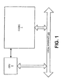
- FIG. 1 illustrates a system incorporating the entropy CODEC of the present invention.
- CPU central processing unit
- FIG. 2 an embodiment of the entropy CODEC 1 of the present invention is illustrated.
- the CODEC 1 operates in two modes: encode mode and decode mode.
- a register interface 100 interfaces with CPU 10 to control the input and reading of data to/from the registers of register block 110.
- a counter 170 is provided for counting the level/number of data words stored in FIFO 160 at a given time. Counter 170 provides input to interrupt controller 180 when the level/number of data words stored in FIFO 160 reaches a value corresponding to counter 17.
- Register block 110 includes a putbits length register 110A, a putbits code register 110B, a FIFO level register 110C, a reset register 110D, a control register 110E, a flush first-in first-out (FLUSH FIFO) register 110F, a get bits register 110G, a bit pointer register 110H and a packed output words register 110I.
- controller 130 which controls operation of a multiplexor 140, a bitstream buffer 150, and a first-in-first-out register block (FIFO) 160. Controller 130 operates in accordance with instructions from CPU 10.
- FIFO 160 is, for example, a 32bit x 16 word FIFO register block.
- Multiplexor 140 is connected to local interface 120 via which data is transferred to and from the register block 110.
- Reset register 110D is a write only register used to reset the hardware, including all pointers and FIFO 160, of the present invention 1.
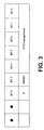
- Control register 110E stores data representing the control bits as illustrated in FIG. 3. With reference to FIG. 3, it can be seen that control register 110E can be configured so that, for example, bits 0-4 represent a pre-defined value, or FIFO interrupt level, which represents a maximum or minimum level/number of data words allowed to be stored in FIFO 160, depending upon the mode of operation.
- Bit 5 of control register 110E is the encode/decode bit (EN/DEC). The value of the EN/DEC bit indicates whether the CODEC 1 is decoding data from the FIFO 160 or encoding data into the FIFO 160.
- control register 110E represents the interrupt enable bit.
- the interrupt enable (IE) bit can be, for example, a 1 (HIGH) that enables the CODEC 1 to interrupt the CPU 10.
- the remaining bits of control register 110E are used to collect variable length code word data. This code word data is subsequently read out from control register 110E and routed to bitstream buffer 150 via multiplexor 140. All bits in the control register 110E will, preferably, default to a 0 upon a reset.
- bitpointer register 110H is provided.
- the bit pointer register 110H is preferably a read only register which, during encode mode, stores data reflecting a pointer value indicating the next available most significant bit (MSB) in bitstream register 150 that can be loaded with data.
- MSB most significant bit
- bitstream buffer 150 is, for example, 32-bits in length
- the bitstream pointer register can point to one of 32 bits, bit 0 through bit 31.
- bitstream pointer will point to bit 0, which indicates that the bitstream buffer 150 is full. If the bitstream pointer register indicates a value between 1 and 31, then bitstream buffer 150 has bits available to accept data input.
- bit pointer register 110H indicates a value of 28
- the value in bit pointer 110H specifies the MSB bit in bitstream buffer 150 in which data can be loaded.
- Flush FIFO register 110F can be addressed to cause data stored in the bitstream buffer 150 to be written into the FIFO 160.
- the contents of bit pointer register 110H should be read out before writing to the flush FIFO register 110F.
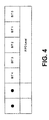
- FIFO level register 110C is illustrated in FIG. 4. Here, it can be seen that bits 0-4 are used to store the FIFO level.
- the FIFO level is a value representative of the number of data words that can be loaded into FIFO 160 before the contents of FIFO 160 will be read out to make room for additional data words.
- the FIFO level register 110C can be read from during both encode and decode modes.
- a putbits code register 110B is provided for storing data representing the next variable bit-length code word to be output or written to the output data string. Data written to the putbits code register 110B is preferably right-justified.
- putbits length register 110A which stores data indicating the number of bits of the putbits code register 110B to be written to the output data string.
- Data written into the putbits length register 110A causes the CODEC 1 to actually write the code data stored in putbits code register 110B.
- data is first written into the putbits code register 110B followed by writing data into the putbits length register 110A.
- Get bits register 10G is used during decode mode to extract variable bit-length codes from the input data stream. For example, where it is desired that the next five bits from the data input stream are to be read, a value of 5 will be written into the get bits register 110G. The five least significant bits of get bits register 110G will then contain the code word.
- a packed output word register 110I is provided.
- Packed output word register 110I can, for example, be accessed/addressed via a controller or central processor (CPU) block read instruction. By reading the data contained in the addressed spaces of packed output word register 110I, the next compressed data word will be output from FIFO 160 to CPU 10.
- CPU central processor
- encode mode data flow is generally flowing from multiplexor 140 to bitstream buffer 150 to FIFO 160.
- decode mode data flow is generally flowing from FIFO 160 to bitstream buffer 150 to multiplexor 140.
- control register 110E In encode mode, data will be written to control register 110E to set the FIFO interrupt level and the interrupt enable bit.
- the encode/decode bit will be set to encode.
- Data to be encoded is loaded into put-bits code register 110B. This data is composed of variable length data words.
- Controller 130 causes multiplexor 140 to select the valid bits from putbits code register 110B for reading the valid bits from the fixed length data word into bitstream buffer 150.
- FIFO register block 160 is associated with a counter 170 which counts the number of 32 bit words contained at any particular time in the FIFO register 160.
- the count value of counter 170 is stored into FIFO level register 110C as FIFO level data.
- This data can be used by the CPU 10 to determine whether or not to read or write data into the FIFO 160. For example, the CPU 10 could poll the FIFO level register and when the FIFO level data stored in FIFO level register 160 corresponds to the FIFO interrupt level data stored in control register 110E, depending upon the mode of operation, the CPU could cause data to be read from or written into the FIFO 160.
- Data can also be read from or written into FIFO 160 where the value of counter 170 corresponds to the contents of the FIFO interrupt level data stored in control register 110E.
- the interrupt controller 180 causes an interrupt signal to be directed to CPU 10 to indicate that it is time for the CPU 10 to read (during encode mode) or write (during decode mode) the contents from/to the FIFO register 160.
- FIG. 5 shows a flowchart illustrating the encode method of the present invention.
- put-bits length register 110A is addressed to cause a code word to be loaded from, for example, the put-bits code register 110B (500).
- the code word is of variable length and may be the result of an entropy coding process.
- Put-bits code register 110B is of a fixed number of bits (length). The length of the variable length code word is stored into putbits length register 110A.
- the variable length code word data loaded into put-bits code register 110B may not require all available storage bits of put-bits code register 110B.
- variable length code word data is loaded into put-bits code register 110B, it may or may not occupy all available bits of the put-bits length register 110B.
- Put-bits code register 110A is, for example, 16 bits in length and a variable length code word of 4 bits is loaded into put-bits code register 110B.
- the 4 bits of put-bits code register 110B that actually store the variable length code word data are said to be valid bits.
- the number of valid bits of put-bits code register 110B is then determined (501) by referring to the data values previously stored in the get bits register 110G. This determination is made via controller 130. However, it is possible for such determination to be carried out by CPU 10. It is then determined whether all of the valid bits will fit into remaining open bits of bitstream buffer 150 (502). If so, these valid bits are loaded into remaining open bits of bitstream buffer 150 (503) and subsequently read out as fixed length data words (511).
- bitstream buffer 150 if the valid bits will not fit into bitstream buffer 150, it will be determined if any of the valid bits will fit into the bitstream buffer 150 (504). Where some of the valid bits will fit into bitstream buffer 150, they (first set of partial valid bits) will be loaded into the bitstream buffer 150 (505) to fill all available bits of bitstream buffer 150. The bitstream buffer contents will then be read out to a first-in/first-out (FIFO) register 160 (506). The bitstream buffer 150 is then clear of any data and the second set of partial valid bits is loaded into the bitstream buffer 150 (507). This process is illustrated in FIG. 7, which is further discussed below.
- the contents of the bitstream buffer 150 will be loaded into FIFO 160 (508). If the FIFO 160 is full (509) the contents thereof will be emptied (510).
- the FIFO 160 is associated with a counter 170.
- Counter 170 maintains a count of, for example, the number of 32-bit words actually loaded into the FIFO 160.
- interrupt controller 180 will cause an interrupt to be generated and directed to CPU 10.
- CPU 10 will read out a predetermined number of words from FIFO 160. This makes room available within FIFO 160 to receive additional code word data from bitstream buffer 150.
- FIG. 6 shows a flowchart illustrating the decode method of the present invention.
- decode mode data will be written to control register 110E to set the FIFO interrupt level and the interrupt enable bit.
- the encode/decode bit will be set to decode.
- Get-bits register 110G is addressed to cause a fixed length data word to be loaded into, for example, FIFO 160.
- Bitstream buffer 150 receives a fixed length data word from FIFO 160.
- the fixed length data word is composed of multiple variable length code words.
- a variable length code word is read out from the bitstream buffer 150 in accordance with data length information stored in get bits register 10G.
- Multiplexor 140 then routes the variable length code word to get bits register 110G from where it is then read out as a fixed length code word.
- bitstream buffer 150 and FIFO 160 Operations of multiplexor 140, bitstream buffer 150 and FIFO 160 are controlled by controller 130 in accordance with data stored in register block 110. Once all variable length code words have been read out from the fixed length code word loaded into bitstream buffer 150, another fixed length code word is retrieved from FIFO 160 and loaded into bitstream buffer 150.
- FIFO 160 is, for example, a 32 bit by 16-word FIFO register.
- Counter 170 maintains a count of the number of data words stored in FIFO 160 at a given time and storing this value into FIFO level register 110C.
- interrupt controller 180 When the value stored in FIFO level register 110C corresponds to a FIFO Interrupt level value stored in control register 110E, interrupt controller 180 generates an interrupt signal. This interrupt signal is directed to the CPU 10, which responds by causing additional fixed length data to be loaded into FIFO 160.
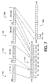
- FIG. 7 illustrates how valid bits of variable length code words are read out of put-bits code register 110B and loaded into bitstream buffer 150 during the encode mode operations of the present invention.
- FIG. 7 also shows how fixed length code words are read out of bitstream buffer 150 and loaded into put-bits code register 110B during the decode mode operations of the present invention.
- Bitstream buffer 150A depicts the status of bitstream buffer 150 after valid bits of variable length of code words, including a first partial set of data, have completely filled the available bits of bitstream register 150.
- Bitstream 150B depicts the status of bitstream buffer 150 after a second partial set of variable length code words have been loaded into the bitstream buffer 150.
- bitstream buffer 150 The initial state of bitstream buffer 150 is clear and all bits are available to receive data. It will be noted that the illustration in FIG. 7 shows bitstream buffer 150 as a 16-bit register. However, in a preferred embodiment, bitstream buffer 150 is 32-bits in length. It will be recognized that bitstream buffer 150 can be any length.
- bitstream buffer 150A With regard to encode mode operations, it can be seen that the valid bits 701-704 of a first code word 700 are loaded into the most significant four (4) bits of bitstream buffer 150 that are available. Subsequently, the valid bits 801-806 of code word 800 are loaded into the next most significant bits of bitstream buffer 150A that are available. Next the valid bits 901-903 of code word 900 are loaded into the next most significant bits of bitstream buffer 150A which are available. In the case of code word 1000, there are six valid bits of data 1001-1007. However, bitstream buffer 150A only has three (3) available bits remaining for receiving data. In this case, bits 1001-1003 are loaded into the remaining available bits of bitstream buffer 150.
- bitstream buffer 150A the contents of bitstream buffer 150A are read out and stored into FIFO 160.
- Bitstream buffer 150 is then clear (150B) and open to receive additional data bits.
- the remaining bits 1004-1006 are then written into the most significant bits of bitstream buffer 150B. This continues until all available bits of bitstream buffer 150 are loaded with valid code word data or, there is no more code word data to be loaded.
- variable length code words 701-704 are read out of bitstream buffer 150A and loaded into put-bits code register 110B.
- Putbits code register 110B is then read out and cleared.
- Variable length code words 801-806 are then read out of bitstream buffer 150A and loaded into putbits code register 110B. This continues until all variable length code words are read out of bitstream buffer 150A.
- variable length code words 1001-1003 are read out and loaded into putbits code register 110B, it is recognized that these bits are only a partial segment of the full code word. In this case, putbits code register 110B is not immediately read out and cleared. However another variable length word is written into bitstream buffer 150B. The second segment of the variable length code word, bits 1004-1006 are then read out of bitstream buffer 150B and loaded into putbits register 110B, which is then read out and cleared of data.
- bitstream register 150 is illustrated herein as a 16-bit register, it can be implemented as any size register as may be suitable for the specific purposes at hand, including but not limited to, for example, an 8-bit register, a 32-bit register or a 64-bit register.
- multiplexor 140 and FIFO 160 can be implemented in whatever bit length desired or determined to be most suitable for the application at hand.
- the method of the present invention can be implemented in hardware, software, firmware, or a combination thereof.
- the method is implemented in software or firmware that is stored in a memory and that is executed by a suitable instruction execution system.
- the method can be implemented with any or a combination of the following technologies, which are all well known in the art: a discrete logic circuit(s) having logic gates for implementing logic functions upon data signals, an application specific integrated circuit (ASIC) having appropriate combinational logic gates, a programmable gate array(s) (PGA), a field programmable gate array (FPGA ), etc.
- each block represents a module, segment, or portion of code, which comprises one or more executable instructions for implementing the specified logical function(s).
- the functions noted in the blocks may occur out of the order noted in FIG. 5 or FIG. 6.
- two blocks shown in succession in FIG. 5 or FIG. 6 may in fact be executed substantially concurrently or the blocks may sometimes be executed in the reverse order, depending upon the functionality involved, as discussed above.
Landscapes
- Engineering & Computer Science (AREA)
- Theoretical Computer Science (AREA)
- Compression, Expansion, Code Conversion, And Decoders (AREA)
- Compression Or Coding Systems Of Tv Signals (AREA)
Claims (4)
- Ein Codierer/Decodierer, der konfiguriert ist, um abwechselnd in einem ersten Betriebsmodus und einem zweiten Betriebsmodus zu arbeiten, wobei der Codierer/Decodierer folgende Merkmale aufweist:wobei das Datenregister (110) konfiguriert ist, um während dem ersten Betriebsmodus ein Codewort variabler Länge zu empfangen und zu speichern, das gültige Datenbits umfasst, die durch einen Entropiecodierungsalgorithmus komprimiert werden, und um während dem zweiten Betriebsmodus Daten, die ein Codewort variabler Länge umfassen, das durch einen Entropiedecodierungsalgorithmus dekomprimiert werden soll, zu empfangen und zu speichern;ein Datenregister (110), das eine vorbestimmte Anzahl von Bits umfasst;ein Bitstromregister (150), das eine vorbestimmte Anzahl von Bits umfasst;einen Multiplexer (140);ein Zuerst-Hinein-Zuerst-Hinaus- (FIFO-) Register (160), das eine Mehrzahl von verfügbaren Mehrbitregistern umfasst;eine Unterbrechungssteuerung (180) zum Erzeugen eines Unterbrechungssignals;
wobei das Bitstromregister (150) konfiguriert ist, um während dem ersten Betriebsmodus Daten zu empfangen und während dem zweiten Betriebsmodus ein codiertes Datenwort fester Länge von dem FIFO-Register (160) zu empfangen;
wobei der Multiplexer konfiguriert ist, um während dem ersten Betriebsmodus zumindest einen Teil der gültigen Bits von dem Datenregister (110) in die höchstwertigsten nichtverwendeten Bits in dem Bitstromregister (150) zu laden, und während dem zweiten Betriebsmodus ein Codewort variabler Länge gemäß einem ausgewählten Wert, der in den Codierer/Decodierer geschrieben ist, von dem Bitstromregister (150) in das Datenregister (110) zu laden;
wobei das FIFO-Register (160) während dem ersten Betriebsmodus konfiguriert ist, um den Inhalt des Bitstromregisters (150) zu empfangen, wenn die vorbestimmte Anzahl von Bits des Bitstromregisters (150) mit einem Teil der gültigen Bits von Daten geladen sind und der Rest der gültigen Bits geladen werden muss;
wobei das FIFO-Register (160) während dem zweiten Betriebsmodus konfiguriert ist, um Daten zu empfangen, die aus dem codierten Datenwort fester Länge bestehen, wobei das Datenwort das Codewort variabler Länge umfasst;
wobei die Unterbrechungssteuerung (180) konfiguriert ist, um während dem ersten Betriebsmodus ein Auslesen von Daten von dem FIFO-Register (160) auszulösen; und
wobei die Unterbrechungssteuerung (180) ferner konfiguriert ist, um während dem zweiten Betriebsmodus das Schreiben des codierten Datenworts fester Länge in das FIFO-Register (160) auszulösen. - Ein Codierer/Decodierer gemäß Anspruch 1, bei dem der Multiplexer (140) ein Barrel-Schieberegister umfasst.
- Ein Codierer/Decodierer gemäß Anspruch 1, der ferner einen Zähler (170) zum Zählen der Anzahl von Mehrbitwörtern umfasst, die in dem FIFO-Register (160) gespeichert sind.
- Ein Codierer/Decodierer gemäß Anspruch 3, bei dem die Unterbrechungssteuerung (180) das Unterbrechungssignal erzeugt, wenn der Zähler (170) einen vorbestimmten Unterbrechungswert erreicht.
Applications Claiming Priority (2)
| Application Number | Priority Date | Filing Date | Title |
|---|---|---|---|
| US565015 | 2000-05-04 | ||
| US09/565,015 US6621428B1 (en) | 2000-05-04 | 2000-05-04 | Entropy codec for fast data compression and decompression |
Publications (2)
| Publication Number | Publication Date |
|---|---|
| EP1154575A1 EP1154575A1 (de) | 2001-11-14 |
| EP1154575B1 true EP1154575B1 (de) | 2005-05-04 |
Family
ID=24256852
Family Applications (1)
| Application Number | Title | Priority Date | Filing Date |
|---|---|---|---|
| EP01102700A Expired - Lifetime EP1154575B1 (de) | 2000-05-04 | 2001-02-07 | Entropie Kodierer/Dekodierer zur schnellen Datenkompression und -dekompression |
Country Status (4)
| Country | Link |
|---|---|
| US (1) | US6621428B1 (de) |
| EP (1) | EP1154575B1 (de) |
| JP (1) | JP2002009625A (de) |
| DE (1) | DE60110493T2 (de) |
Families Citing this family (11)
| Publication number | Priority date | Publication date | Assignee | Title |
|---|---|---|---|---|
| US6781589B2 (en) * | 2001-09-06 | 2004-08-24 | Intel Corporation | Apparatus and method for extracting and loading data to/from a buffer |
| WO2004036433A1 (ja) * | 2002-10-21 | 2004-04-29 | Renesas Thchnology Corp. | 半導体集積回路装置 |
| JP4336678B2 (ja) * | 2003-09-04 | 2009-09-30 | 株式会社日立超エル・エス・アイ・システムズ | 半導体装置 |
| US7161507B2 (en) * | 2004-08-20 | 2007-01-09 | 1St Works Corporation | Fast, practically optimal entropy coding |
| US7265691B2 (en) * | 2005-06-23 | 2007-09-04 | 1Stworks Corporation | Modeling for enumerative encoding |
| US7728742B2 (en) * | 2008-09-30 | 2010-06-01 | Apple Inc. | Method and apparatus for compressing and decompressing data |
| US7800519B2 (en) * | 2008-09-30 | 2010-09-21 | Apple Inc. | Method and apparatus for compressing and decompressing data |
| US8194755B2 (en) * | 2009-03-06 | 2012-06-05 | Himax Media Solutions, Inc. | Bit stream buffer controller and its method |
| CN104011660B (zh) * | 2011-12-22 | 2017-03-01 | 英特尔公司 | 用于处理位流的基于处理器的装置和方法 |
| US9606961B2 (en) * | 2012-10-30 | 2017-03-28 | Intel Corporation | Instruction and logic to provide vector compress and rotate functionality |
| EP2940575B1 (de) * | 2014-05-02 | 2018-05-09 | Nxp B.V. | Steuerungsschaltungen, Datenschnittstellenblöcke und Verfahren zur Übertragung von Daten |
Family Cites Families (7)
| Publication number | Priority date | Publication date | Assignee | Title |
|---|---|---|---|---|
| US4376933A (en) | 1979-02-22 | 1983-03-15 | Xerox Corporation | Circuit for compacting data |
| US4360840A (en) | 1980-05-13 | 1982-11-23 | Am International, Inc. | Real time data compression/decompression scheme for facsimile transmission system |
| US5237701A (en) * | 1989-03-31 | 1993-08-17 | Ampex Systems Corporation | Data unpacker using a pack ratio control signal for unpacked parallel fixed m-bit width into parallel variable n-bit width word |
| US4963867A (en) * | 1989-03-31 | 1990-10-16 | Ampex Corporation | Apparatus for packing parallel data words having a variable width into parallel data words having a fixed width |
| JPH03106127A (ja) | 1989-09-20 | 1991-05-02 | Fujitsu Ltd | 可変長符号化回路 |
| US5499382A (en) | 1993-09-20 | 1996-03-12 | Nusinov; Eugene B. | Circuit and method of bit-packing and bit-unpacking using a barrel shifter |
| JP2715871B2 (ja) * | 1993-12-20 | 1998-02-18 | 日本電気株式会社 | 可変長符号化方法 |
-
2000
- 2000-05-04 US US09/565,015 patent/US6621428B1/en not_active Expired - Fee Related
-
2001
- 2001-02-07 DE DE60110493T patent/DE60110493T2/de not_active Expired - Lifetime
- 2001-02-07 EP EP01102700A patent/EP1154575B1/de not_active Expired - Lifetime
- 2001-04-23 JP JP2001124175A patent/JP2002009625A/ja active Pending
Also Published As
| Publication number | Publication date |
|---|---|
| US6621428B1 (en) | 2003-09-16 |
| DE60110493D1 (de) | 2005-06-09 |
| EP1154575A1 (de) | 2001-11-14 |
| JP2002009625A (ja) | 2002-01-11 |
| DE60110493T2 (de) | 2006-01-05 |
Similar Documents
| Publication | Publication Date | Title |
|---|---|---|
| KR100227275B1 (ko) | 단위 처리 시스템에서의 가변길이코드 검출장치 및 방법 | |
| US5710562A (en) | Method and apparatus for compressing arbitrary data | |
| US6798833B2 (en) | Video frame compression/decompression hardware system | |
| US7936938B2 (en) | Methods and devices for encoding a digital image signal and associated decoding methods and devices | |
| EP0313191B1 (de) | Datenkomprimierungssystem mit Expandierungsschutz | |
| EP1410509B1 (de) | Nicht auf zweierpotenz basierendes gray-code zählersystem mit einem binären incrementierer mit zweiseitig symmetrisch verteilten zahlen | |
| EP1154575B1 (de) | Entropie Kodierer/Dekodierer zur schnellen Datenkompression und -dekompression | |
| JP3294026B2 (ja) | 高速可変長復号化装置 | |
| WO1995019662A1 (en) | Data compression apparatus and method | |
| US20050152609A1 (en) | Video decoder | |
| EP0587324B1 (de) | Vorrichtung zur Datenformatierung | |
| US6809665B2 (en) | Apparatus and method for decoding variable length code | |
| US6285789B1 (en) | Variable length code decoder for MPEG | |
| EP0742646B1 (de) | Datenkompressionsverfahren und Vorrichtung mit Expansionsschutz | |
| US6408102B1 (en) | Encoding/decoding device | |
| US5781135A (en) | High speed variable length code decoder | |
| US5488366A (en) | Segmented variable length decoding apparatus for sequentially decoding single code-word within a fixed number of decoding cycles | |
| CN100433560C (zh) | 包含cpu处理器接口的可编程变长解码器 | |
| US6320521B1 (en) | System and method for efficiently merging compressed data | |
| JP3450553B2 (ja) | 可変長符号復号装置 | |
| US5686914A (en) | Information processing system | |
| US5822552A (en) | Method and circuit for rearranging output data in variable-length decoder | |
| US6496602B2 (en) | Sorting device of variable-length code | |
| US5822770A (en) | Memory interfacing method and circuit of variable length decoder for accessing external memory when empty portion of internal memory exceeds a predetermined level | |
| GB2311704A (en) | Compression of arbitrary data using context modelling and entropy coding |
Legal Events
| Date | Code | Title | Description |
|---|---|---|---|
| PUAI | Public reference made under article 153(3) epc to a published international application that has entered the european phase |
Free format text: ORIGINAL CODE: 0009012 |
|
| 17P | Request for examination filed |
Effective date: 20010823 |
|
| AK | Designated contracting states |
Kind code of ref document: A1 Designated state(s): AT BE CH CY DE DK ES FI FR GB GR IE IT LI LU MC NL PT SE TR Kind code of ref document: A1 Designated state(s): DE FR GB |
|
| AX | Request for extension of the european patent |
Free format text: AL;LT;LV;MK;RO;SI |
|
| 17Q | First examination report despatched |
Effective date: 20020131 |
|
| AKX | Designation fees paid |
Free format text: DE FR GB |
|
| GRAP | Despatch of communication of intention to grant a patent |
Free format text: ORIGINAL CODE: EPIDOSNIGR1 |
|
| GRAS | Grant fee paid |
Free format text: ORIGINAL CODE: EPIDOSNIGR3 |
|
| GRAA | (expected) grant |
Free format text: ORIGINAL CODE: 0009210 |
|
| AK | Designated contracting states |
Kind code of ref document: B1 Designated state(s): DE FR GB |
|
| REG | Reference to a national code |
Ref country code: GB Ref legal event code: FG4D |
|
| REF | Corresponds to: |
Ref document number: 60110493 Country of ref document: DE Date of ref document: 20050609 Kind code of ref document: P |
|
| PLBE | No opposition filed within time limit |
Free format text: ORIGINAL CODE: 0009261 |
|
| STAA | Information on the status of an ep patent application or granted ep patent |
Free format text: STATUS: NO OPPOSITION FILED WITHIN TIME LIMIT |
|
| ET | Fr: translation filed | ||
| 26N | No opposition filed |
Effective date: 20060207 |
|
| PGFP | Annual fee paid to national office [announced via postgrant information from national office to epo] |
Ref country code: FR Payment date: 20070221 Year of fee payment: 7 |
|
| REG | Reference to a national code |
Ref country code: FR Ref legal event code: ST Effective date: 20081031 |
|
| PG25 | Lapsed in a contracting state [announced via postgrant information from national office to epo] |
Ref country code: FR Free format text: LAPSE BECAUSE OF NON-PAYMENT OF DUE FEES Effective date: 20080229 |
|
| PGFP | Annual fee paid to national office [announced via postgrant information from national office to epo] |
Ref country code: DE Payment date: 20100226 Year of fee payment: 10 Ref country code: GB Payment date: 20100224 Year of fee payment: 10 |
|
| GBPC | Gb: european patent ceased through non-payment of renewal fee |
Effective date: 20110207 |
|
| REG | Reference to a national code |
Ref country code: DE Ref legal event code: R119 Ref document number: 60110493 Country of ref document: DE Effective date: 20110901 |
|
| PG25 | Lapsed in a contracting state [announced via postgrant information from national office to epo] |
Ref country code: GB Free format text: LAPSE BECAUSE OF NON-PAYMENT OF DUE FEES Effective date: 20110207 |
|
| PG25 | Lapsed in a contracting state [announced via postgrant information from national office to epo] |
Ref country code: DE Free format text: LAPSE BECAUSE OF NON-PAYMENT OF DUE FEES Effective date: 20110901 |