EP1152340A2 - System and method for observing information transmitted between two integrated circuits - Google Patents
System and method for observing information transmitted between two integrated circuits Download PDFInfo
- Publication number
- EP1152340A2 EP1152340A2 EP01106703A EP01106703A EP1152340A2 EP 1152340 A2 EP1152340 A2 EP 1152340A2 EP 01106703 A EP01106703 A EP 01106703A EP 01106703 A EP01106703 A EP 01106703A EP 1152340 A2 EP1152340 A2 EP 1152340A2
- Authority
- EP
- European Patent Office
- Prior art keywords
- integrated circuit
- data port
- data
- port
- communication link
- Prior art date
- Legal status (The legal status is an assumption and is not a legal conclusion. Google has not performed a legal analysis and makes no representation as to the accuracy of the status listed.)
- Withdrawn
Links
Images


Classifications
-
- G—PHYSICS
- G06—COMPUTING OR CALCULATING; COUNTING
- G06F—ELECTRIC DIGITAL DATA PROCESSING
- G06F11/00—Error detection; Error correction; Monitoring
- G06F11/36—Prevention of errors by analysis, debugging or testing of software
- G06F11/362—Debugging of software
- G06F11/3636—Debugging of software by tracing the execution of the program
Definitions
- computers are capable of operating at frequencies in the high megahertz to gigahertz range.
- the technology relating to analyzing devices such as logic analyzers or oscilloscopes, has not increased in such magnitude. Rather, most analyzing devices are not capable of operating at frequencies in the mid megahertz to low gigahertz range.
- interconnecting an analyzer device directly to communication lines within a present day electronics system will disrupt and disturb the normal operation of the system, perhaps rendering the system inoperable.
- the present invention provides a system and method for observing bi-directional information transmitted on a first and a second communication link between a first and a second integrated circuit to determine proper operation of the communication links and integrated circuits such that the performance of the overall system is not inhibited.
- the second data ports of the second and third integrated circuits are dedicated debugging ports, solely for facilitating an analyzing function.
- the debugging ports of the second and third integrated circuits may be standard data ports capable of facilitating the communication of data between the second and third integrated circuits, respectfully, and other electrical components or integrated circuits of the overall system.
- the second ports of the second and third integrated circuits may each include in the range of approximately 50-250 data pins.
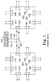
- Figure 1 illustrates a standard technique used to directly observe data within bi-directional communication links of a data bus between two integrated circuits to verify the integrity of the system.
- Integrated circuit 100 includes data ports 102, 104, 106, 108, 110, 112, 114, and 116.
- Integrated circuit 120 includes data ports 122, 124, 126, 128, 130, 132, 134, and 136.
- Each data port of data ports 102-116 and 122-136 include bi-directional capabilities such that a first communication link connected to each port facilitates data communication out of the data port while a second communication link connected to the data port facilitates communication of data into the data port.
- communication links can be associated with one or more data ports, such as data ports 102-116 and 122-136. However, these communication links are not labeled for clarity purposes. It is also understood that each communication link may be electrically coupled tc other communication links within a particular integrated circuit, or may be electrically coupled to various electrical components or subsystems within a given integrated circuit. It is further understood that numerous integrated circuits may be electrically coupled to one another through use of one or more printed circuit boards electrically coupling the integrated circuits.
- debugging port 164 and 168 each include in the range of approximately 50-250 data pins. Therefore, a maximum number of output pins of an integrated circuit can be used for operational purposes, rather than analyzation purposes.
- debugging port 168 of integrated circuit 156 can not be simultaneously used for debugging purposes of integrated circuit 156.
- a debugging port of an integrated circuit such as integrated circuit 156, is not used. Perhaps due to the nature of the integrated circuit and its interconnections, there is not reason to debug any aspect of the integrated circuit.
- debugging port 168 of integrated circuit 156 may alternatively provide debugging information for integrated circuits 152 and 156 via additional electrical connections within integrated circuit 156 to debugging port 168 not shown for clarity purposes.
- FIG. 3 is an electrical diagram illustrating another embodiment of the present invention.
- System 200 shown in Figure 3, includes integrated circuits 202, 204, 206, and 208, and microprocessors 210, 212, 214, 216, 218, 220, 222, and 224.
- System 200 shown in Figure 3, is similar to system 150, shown in Figure 2, in that data information on a communication link between two integrated circuits is provided to a third integrated circuit for electrically coupling the data to analyzation equipment.
- the debugging ports of all integrated circuits are electrically coupled to other communication links or that the debugging ports cannot facilitate the transfer of data information due to quantity and speed constraints. Therefore, the communication links to be analyzed are electrically coupled to other data ports of integrated circuits which are either not used at all or not used within specific time intervals.
- communication links 226 and 228 are interconnected between ports 230 and 232 of integrated circuits 202 and 204, respectively.
- debugging port 234 of integrated circuit 202 is dedicated to electrically coupling data from communication link 236 to an external source.
- debugging port 234 of integrated circuit 202 is not available.
- a portion of the data from communication link 228 is electrically coupled to debugging port 238 of integrated circuit 204 via link 240.
- some integrated circuit chips, such as integrated circuit 204 are designed such that their debugging ports include a minimal number output pins, for reasons previously discussed. Therefore, all information from communication link 228 cannot be forwarded out of debugging port 238 at the frequency of the system.
- integrated circuit 204 can be electrically coupled to numerous integrated circuits or microprocessors, such as up to 16 or 32 microprocessors.
- microprocessors such as up to 16 or 32 microprocessors.
- some communication links or data buses, such as communication link 250 is not utilized. Therefore, analyzation equipment, such as analyzation equipment 144, can be electrically coupled to communication link 250 as previously discussed.
- data buses or communication links 242, 244, 246, and 248 analyzation equipment can be connected to these communication links at times in which microprocessors 210, 212, 214, and 216 are not operating. Thus, during non-operational time intervals, debugging information can be transmitted on these lines.
- communication links 226 and 228 can be electrically coupled to any data port of integrated circuit 204 not currently being used, such as the data ports associated with links 242, 244, 246, 248, and 250.
- An analyzation device can be coupled to the specific port and diagnostic functions can be completed.
Landscapes
- Engineering & Computer Science (AREA)
- Theoretical Computer Science (AREA)
- Computer Hardware Design (AREA)
- Quality & Reliability (AREA)
- Physics & Mathematics (AREA)
- General Engineering & Computer Science (AREA)
- General Physics & Mathematics (AREA)
- Tests Of Electronic Circuits (AREA)
- Semiconductor Integrated Circuits (AREA)
- Test And Diagnosis Of Digital Computers (AREA)
Abstract
Description
Claims (15)
- A system for observing bi-directional information transmitted on a first and a second communication link electrically connected to a first integrated circuit, the system comprising:a second integrated circuit electrically coupled to the first and second communication links, the second integrated circuit further comprising:a first data port electrically coupled to the first and second communication links;a second data port electrically coupled to the first communication link of the first data port;a third data port electrically coupled to the second communication link of the first data port, the third data port capable of electrical connection with an analyzing device;a third integrated circuit further comprising:a first data port;a second data port electrically coupled to the first data port, the second data port capable of electrical connection with the analyzing device; anda third communication link electrically coupling the second data port of the second integrated circuit to the second data port of the third integrated circuit.
- The system of claim 1, wherein the third data port of the second integrated circuit is a dedicated debugging port.
- The system of claim 1 or 2, wherein the second data port of the third integrated circuit is a dedicated debugging port.
- The system of one of the preceding claims, wherein the first communication link is a dedicated input link and the second communication link is a dedicated output link.
- The system of one of the preceding claims, wherein the third data port of the second integrated circuit includes in the range of approximately 50-250 data pins.
- The system of one of the preceding claims, wherein t integrated circuit includes in the range of approximately 50-250 data pins.
- A system for observing bi-directional information transmitted on a first and a second communication link between a first data port of a first integrated circuit and a first data port of a second integrated circuit, the system comprising:a second data port of the second integrated circuit, the second data port electrically coupled to the first data port of the second integrated circuit for receiving information from the first communication link, the second data port capable of electrical connection with an analyzing device;a third data port of the second integrated circuit, the third data port electrically coupled to the first data port of the second integrated circuit for receiving information from the second communication link;a third communication link electrically coupling the third data port of the second integrated circuit to a first data port of a third integrated circuit; anda second data port of the third integrated circuit, the second data port electrically coupled to the first data port of the third integrated circuit for receiving information from the second communication link, the second data port capable of electrical connection with the analyzing device.
- The system of claim 7, wherein the second data port of the second integrated circuit is a dedicated debugging port.
- The system of claim 7 or 8, wherein the second data port of the third integrated circuit is a dedicated debugging port.
- The system of one of claims 7 to 9, wherein the first communication link is a dedicated input link and the second communication link is a dedicated output link.
- The system of one of claims 7 to 10, wherein the second data port of the second integrated circuit includes in the range of approximately 50-250 data pins.
- The system of one of claims 7 to 11, wherein the second data port of the third integrated circuit includes in the range of approximately 50-250 data pins.
- A method of observing bi-directional information transmitted on a first and a second communication link electrically connected between a first data port of a first integrated circuit and a first data port of a second integrated circuit, the method comprising:electrically coupling the first communication link from the first data port of the second integrated circuit to a second data port of the second integrated circuit;electrically coupling the second communication link from the first data port of the second integrated circuit to a third data port of the second integrated circuit;electrically coupling the second communication link from the third data port to a first data port of a third integrated circuit;electrically coupling the second communication link from the first data port of the third integrated circuit to a second data port of the third integrated circuit; andwherein observation of the first communication link at the second port of the second integrated circuit and the second communication at the second data port of the third integrated circuit is achieved by an analyzing device electrically coupled to the second data ports of the second and third integration circuits.
- The method of claim 13, wherein the step of electrically coupling the first communication link from the first data port of the second integrated circuit to the second data port of the second integrated circuit further comprises:
electrically coupling either one of a dedicated input link or a dedicated output link from the first data port of the second integrated circuit to a dedicated debugging port of the second integrated circuit. - The method of claim 13 or 14, wherein the step of electrically coupling the second communication link from the first data port of the third integrated circuit to a second data port of the third integrated circuit further comprises:
electrically coupling either one of a dedicated input link or a dedicated output link from the first data port of the third integrated circuit to a dedicated debugging port of the third integrated circuit.
Applications Claiming Priority (2)
| Application Number | Priority Date | Filing Date | Title |
|---|---|---|---|
| US561723 | 1995-11-22 | ||
| US09/561,723 US6300787B1 (en) | 2000-05-01 | 2000-05-01 | System and method for observing information transmitted between two integrated circuits |
Publications (2)
| Publication Number | Publication Date |
|---|---|
| EP1152340A2 true EP1152340A2 (en) | 2001-11-07 |
| EP1152340A3 EP1152340A3 (en) | 2004-08-18 |
Family
ID=24243153
Family Applications (1)
| Application Number | Title | Priority Date | Filing Date |
|---|---|---|---|
| EP01106703A Withdrawn EP1152340A3 (en) | 2000-05-01 | 2001-03-15 | System and method for observing information transmitted between two integrated circuits |
Country Status (2)
| Country | Link |
|---|---|
| US (1) | US6300787B1 (en) |
| EP (1) | EP1152340A3 (en) |
Families Citing this family (5)
| Publication number | Priority date | Publication date | Assignee | Title |
|---|---|---|---|---|
| US7200671B1 (en) * | 2000-08-23 | 2007-04-03 | Mks Instruments, Inc. | Method and apparatus for monitoring host to tool communications |
| US6862647B1 (en) | 2002-01-29 | 2005-03-01 | Advanced Micro Devices, Inc. | System and method for analyzing bus transactions |
| US7328375B2 (en) * | 2003-12-30 | 2008-02-05 | Intel Corporation | Pass through debug port on a high speed asynchronous link |
| US7146237B2 (en) * | 2004-04-07 | 2006-12-05 | Mks Instruments, Inc. | Controller and method to mediate data collection from smart sensors for fab applications |
| US7787477B2 (en) * | 2005-07-11 | 2010-08-31 | Mks Instruments, Inc. | Address-transparent device and method |
Family Cites Families (4)
| Publication number | Priority date | Publication date | Assignee | Title |
|---|---|---|---|---|
| US5905738A (en) * | 1991-05-19 | 1999-05-18 | Texas Instruments Incorporated | Digital bus monitor integrated circuits |
| US5390191A (en) * | 1992-01-31 | 1995-02-14 | Sony Corporation | Apparatus and method for testing the interconnection between integrated circuits |
| US5600790A (en) * | 1995-02-10 | 1997-02-04 | Research In Motion Limited | Method and system for loading and confirming correct operation of an application program in a target system |
| US6233613B1 (en) * | 1997-08-18 | 2001-05-15 | 3Com Corporation | High impedance probe for monitoring fast ethernet LAN links |
-
2000
- 2000-05-01 US US09/561,723 patent/US6300787B1/en not_active Expired - Fee Related
-
2001
- 2001-03-15 EP EP01106703A patent/EP1152340A3/en not_active Withdrawn
Also Published As
| Publication number | Publication date |
|---|---|
| EP1152340A3 (en) | 2004-08-18 |
| US6300787B1 (en) | 2001-10-09 |
Similar Documents
| Publication | Publication Date | Title |
|---|---|---|
| EP0808461B1 (en) | Jtag testing of buses using plug-in cards with jtag logic mounted thereon | |
| US7589548B2 (en) | Design-for-test micro probe | |
| EP1308736B1 (en) | Test circuit and semiconductor integrated circuit effectively carrying out verification of connection of nodes | |
| JP2010519548A5 (en) | ||
| US8020058B2 (en) | Multi-chip digital system having a plurality of controllers with self-identifying signal | |
| US6300787B1 (en) | System and method for observing information transmitted between two integrated circuits | |
| US6260163B1 (en) | Testing high I/O integrated circuits on a low I/O tester | |
| US7478298B2 (en) | Method and system for backplane testing using generic boundary-scan units | |
| US11293979B2 (en) | Method of and an arrangement for analyzing manufacturing defects of multi-chip modules made without known good die | |
| EP0682259A1 (en) | Circuit-test fixture that includes shorted-together probes | |
| US6624625B2 (en) | Test equipment | |
| TWI676040B (en) | Semiconductor integrated circuit test system and semiconductor integrated circuit test device thereof | |
| US6433628B1 (en) | Wafer testable integrated circuit | |
| JP4278360B2 (en) | Multi-chip package LSI test circuit | |
| CN110824330A (en) | Semiconductor integrated circuit test system and semiconductor integrated circuit test device thereof | |
| US20040064763A1 (en) | Apparatus and method for a trace system on a chip having multiple processing units | |
| JP3640671B2 (en) | Apparatus and method for checking the connection between the output of a means for outputting a fixed logic value and the input of a circuit | |
| US7478005B2 (en) | Technique for testing interconnections between electronic components | |
| JP3616306B2 (en) | Semiconductor integrated circuit | |
| CN221650409U (en) | Adapter card, OAM card test system and OAM card working system | |
| JPS6235644A (en) | Semiconductor device | |
| KR200296468Y1 (en) | multi-port socket of the target board | |
| JPH09159728A (en) | Printed circuit board test method | |
| JPH1038977A (en) | Incorporated integrated circuit | |
| JP2002090425A (en) | Failure diagnosis apparatus and method |
Legal Events
| Date | Code | Title | Description |
|---|---|---|---|
| PUAI | Public reference made under article 153(3) epc to a published international application that has entered the european phase |
Free format text: ORIGINAL CODE: 0009012 |
|
| AK | Designated contracting states |
Kind code of ref document: A2 Designated state(s): AT BE CH CY DE DK ES FI FR GB GR IE IT LI LU MC NL PT SE TR |
|
| AX | Request for extension of the european patent |
Free format text: AL;LT;LV;MK;RO;SI |
|
| PUAL | Search report despatched |
Free format text: ORIGINAL CODE: 0009013 |
|
| AK | Designated contracting states |
Kind code of ref document: A3 Designated state(s): AT BE CH CY DE DK ES FI FR GB GR IE IT LI LU MC NL PT SE TR |
|
| AX | Request for extension of the european patent |
Extension state: AL LT LV MK RO SI |
|
| RIC1 | Information provided on ipc code assigned before grant |
Ipc: 7G 06F 11/36 B Ipc: 7G 06F 11/267 B Ipc: 7G 06F 11/22 A |
|
| 17P | Request for examination filed |
Effective date: 20050119 |
|
| AKX | Designation fees paid |
Designated state(s): DE FR GB |
|
| RBV | Designated contracting states (corrected) |
Designated state(s): DE FR GB |
|
| STAA | Information on the status of an ep patent application or granted ep patent |
Free format text: STATUS: THE APPLICATION IS DEEMED TO BE WITHDRAWN |
|
| 18D | Application deemed to be withdrawn |
Effective date: 20060721 |