EP1150402A2 - Laserbearbeitungsvorrichtung - Google Patents
Laserbearbeitungsvorrichtung Download PDFInfo
- Publication number
- EP1150402A2 EP1150402A2 EP01303664A EP01303664A EP1150402A2 EP 1150402 A2 EP1150402 A2 EP 1150402A2 EP 01303664 A EP01303664 A EP 01303664A EP 01303664 A EP01303664 A EP 01303664A EP 1150402 A2 EP1150402 A2 EP 1150402A2
- Authority
- EP
- European Patent Office
- Prior art keywords
- laser
- output
- signal
- power
- excitation light
- Prior art date
- Legal status (The legal status is an assumption and is not a legal conclusion. Google has not performed a legal analysis and makes no representation as to the accuracy of the status listed.)
- Withdrawn
Links
Images


Classifications
-
- H—ELECTRICITY
- H01—ELECTRIC ELEMENTS
- H01S—DEVICES USING THE PROCESS OF LIGHT AMPLIFICATION BY STIMULATED EMISSION OF RADIATION [LASER] TO AMPLIFY OR GENERATE LIGHT; DEVICES USING STIMULATED EMISSION OF ELECTROMAGNETIC RADIATION IN WAVE RANGES OTHER THAN OPTICAL
- H01S3/00—Lasers, i.e. devices using stimulated emission of electromagnetic radiation in the infrared, visible or ultraviolet wave range
- H01S3/10—Controlling the intensity, frequency, phase, polarisation or direction of the emitted radiation, e.g. switching, gating, modulating or demodulating
- H01S3/13—Stabilisation of laser output parameters, e.g. frequency or amplitude
- H01S3/131—Stabilisation of laser output parameters, e.g. frequency or amplitude by controlling the active medium, e.g. by controlling the processes or apparatus for excitation
- H01S3/1312—Stabilisation of laser output parameters, e.g. frequency or amplitude by controlling the active medium, e.g. by controlling the processes or apparatus for excitation by controlling the optical pumping
-
- H—ELECTRICITY
- H01—ELECTRIC ELEMENTS
- H01S—DEVICES USING THE PROCESS OF LIGHT AMPLIFICATION BY STIMULATED EMISSION OF RADIATION [LASER] TO AMPLIFY OR GENERATE LIGHT; DEVICES USING STIMULATED EMISSION OF ELECTROMAGNETIC RADIATION IN WAVE RANGES OTHER THAN OPTICAL
- H01S3/00—Lasers, i.e. devices using stimulated emission of electromagnetic radiation in the infrared, visible or ultraviolet wave range
- H01S3/09—Processes or apparatus for excitation, e.g. pumping
- H01S3/091—Processes or apparatus for excitation, e.g. pumping using optical pumping
- H01S3/0912—Electronics or drivers for the pump source, i.e. details of drivers or circuitry specific for laser pumping
Definitions
- the present invention relates to a waveform-controlled laser processing apparatus.
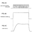
- Fig. 6 shows a major configuration of a conventional waveform-controlled laser processing apparatus.
- the laser processing apparatus comprises a laser oscillation unit 100, a laser power supply unit 102 and a control unit 104.
- the laser power supply unit 102 is electrically connected via a switching element 106 typically formed of a transistor to an excitation light source not shown of a laser oscillation unit 100 so that a DC power or current supplied from the laser power supply unit 102 to the excitation light source is waveform controlled by providing a feedback switching control of the switching element 106 by the control unit 104.
- the laser oscillation unit 100 excites a solid-state laser medium not shown by energy of a light emitted from the excitation light source, to thereby oscillatorily output a laser beam LB having a controlled laser output (light intensity) waveform.
- the control unit 104 includes a laser output measurement unit 108 for measuring an output of the laser beam LB, and a switching control unit 112 for providing a switching control of the switching element 106 on the basis of an error between a feedback signal which is a measured-value-of-laser-output signal ML from the laser output measurement unit 108 and a reference signal M ref from a reference signal generation unit 110.
- an error amplifier 122 consisting of an operational amplifier 114, input resistors 116 and 118 and a feedback resistor 120 compares levels of the two signals ML and M ref with each other to generate an error signal er indicative of the error or difference therebetween, and a PWM (pulse-width modulation) circuit 124 generates a PWM signal MW of a predetermined frequency having a pulse width in conformity with the error signal.
- the PWM signal MW is fed as a switching control signal via a drive circuit 126 to the switching element 106.
- the output of the laser beam LB may have a phase lag to a large extent, e.g., as much as about 180 degrees relative to the switching control signal MW fed for waveform control from the PWM circuit 124 to the switching element 106.
- a phase compensation circuit consisting of a capacitor 128 and a resistor 130 in series, is disposed in parallel with the resistor 120 in a feedback circuit of the operational amplifier 114 so as to strengthen the negative feedback of, esp., high frequency components to thereby compensate a large phase lag almost likely to reverse the phase as described above.
- both the measured-value-of-laser-output signal ML and the reference signal M ref tend to contain a plenty of high frequency components, so that the gain or sensitivity of the error signal er for the error (difference) between the respective high frequency components may become lower with a reduced response speed of the PWM circuit 124.
- This may often bring about a slow rise of the laser output as shown in Figs. 7A to 7C and an overshoot as its reaction with impaired accuracy and reliability in the waveform control. Also from the viewpoint of laser processing quality, it was undesirable.
- the present invention was conceived in view of such problems involved in the prior art. It is therefore an object of the present invention to provide a laser processing apparatus having enhanced accuracy or reliability in the laser output waveform control.
- a laser processing apparatus having a laser oscillation unit exciting a solid-state laser medium by energy of an excitation light emitted from an excitation light source to thereby oscillatorily output a laser beam, a laser power supply unit supplying a power to the excitation light source, and laser output measurement means measuring an output of the laser light, the output of the laser light being controlled on the basis of an error between a feedback signal and a preset reference value, the feedback signal being a laser power measured value from the laser output measurement means, the laser processing apparatus comprising power measuring means arranged to measure a power supplied to the excitation light source, wherein the feedback signal is corrected by an AC component of a signal indicative of a power measured value from the power measuring means so as to control the output of the laser light.
- the measured-value-of-laser-output signal or the feedback signal whose phase significantly lags relative to the control signal is corrected by the AC component of the measured-value-of-power signal substantially in phase with the control signal whereby the feedback signal can have a compensated phase to stabilize the power feedback loop.
- the reference value may be corrected by an AC component of the measured-value-of-power signal to control the output of the laser light.
- arrangement may be such that in place of the power measuring means there are provided current measuring means for measuring a current supplied to the excitation light source so that the feedback signal can be corrected by an AC component of a signal indicative of a power measured value from the power measuring means to thereby control the laser light output.
- the reference value may be corrected by the AC component of the measured-value-of-power signal to thereby control the laser light output.
- the laser processing apparatus of the present invention further comprises switching means connected between the laser power supply unit and the excitation light source; and switching control means arranged to provide a switching control of the switching means at a predetermined frequency by pulse-width modulation.
- the switching means include an adder which adds an AC component of the measured value signal to the feedback signal; an operational amplifier which compares an output signal from the adder with the reference value to amplify an error therebetween; and a capacitor for phase compensation disposed in a feedback circuit of the operational amplifier.
- the switching means may include a subtractor which subtracts an AC component of the measured value signal from the reference value; an operational amplifier which compares an output signal from the subtractor with the feedback signal to amplify an error therebetween; and a capacitor for phase compensation disposed in a feedback circuit of the operational amplifier.
- the phase of the feedback signal is compensated by the AC component of the measured-value-of-power signal or the measured-value-of-current signal so as to stabilize the power feedback loop, with the result that it is possible to render rapidly responsive the frequency characteristics of the operational amplifier constituting the error amplifier to thereby provide a stable and rapid-response laser output waveform control.
- Figs. 1 to 5 illustrate a presently preferred embodiment thereof in a non-limitative manner.
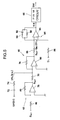
- Fig. 1 depicts the configuration of a principal part of a laser processing apparatus in accordance with the embodiment of the present invention.
- the laser processing apparatus comprises a laser oscillation unit 10, a laser power supply unit 12, a laser cooling unit 14 and a control unit 16.
- the laser oscillation unit 10 includes an excitation lamp 20 acting as an excitation light source and an YAG rod 22 acting as a laser medium which are both arranged within a chamber 18, and a pair of mirrors 24 and 26 disposed in an optical axis of the YAG rod 22 outside the chamber 18.
- the YAG rod 22 When the excitation lamp 20 lights and emits an excitation light, the YAG rod 22 is excited by energy of the excitation light. The light emanating onto the optical axis from the opposite ends of the YAG rod 22 is iteratively reflected for amplification between the optical resonator mirrors 24 and 26 and then passes through the output mirror 24 in the form of a pulsed laser beam LB. After passing through the output mirror 24, the pulsed laser beam LB is sent via an optical transmission system not shown consisting of e.g., a reflection mirror and an optical fiber to a laser output unit not shown at a site to be laser processed and is irradiated from the laser output unit onto a workpiece not shown.
- an optical transmission system not shown consisting of e.g., a reflection mirror and an optical fiber to a laser output unit not shown at a site to be laser processed and is irradiated from the laser output unit onto a workpiece not shown.
- the laser power supply unit 12 includes a capacitor 28 for storing laser oscillation powers to be supplied to the laser oscillation unit 10, and a charging circuit 30 for converting a commercial AC, e.g., three-phase AC power supply voltage (U, V, W) into a direct current to thereby charge the capacitor 28 up to a predetermined DC voltage.
- An output terminal of the laser power supply unit 12, i.e., one terminal of the capacitor 28 is electrically connected via a switching element, e.g., an IGBT (insulated gate bipolar transistor) 32 to the excitation lamp 20.
- a switching element e.g., an IGBT (insulated gate bipolar transistor) 32 to the excitation lamp 20.
- the laser cooling unit 14 serves to discharge heat generated by the excitation lamp 20 and the YAG rod 22 of the laser oscillation unit 10 to the exterior and is arranged to supply a coolant, e.g., a cooling water CW having a controlled temperature to the laser oscillation unit 10.
- a coolant e.g., a cooling water CW having a controlled temperature
- the control unit 16 includes a CPU (microprocessor) 34 for providing a control of operations of the entire apparatus and of each unit, a memory 36 for storing various programs, various set values and other data required to cause the CPU 34 to effect predetermined processings, and various measuring means 38 to 48 and a switching control unit 50 for waveform control.
- a CPU microprocessor
- a laser output measurement unit 38 has a photosensor receiving a laser beam LB' leaking backward from the optical resonator mirror 26, and a measuring circuit determining the laser output of the pulsed laser beam LB on the basis of an electric signal output from the photosensor.
- the laser output measurement unit 38 feeds a measured-value-of-laser-output signal SL acquired from the measuring circuit to both the switching control unit 50 and the CPU 34.
- a voltage measuring circuit 40 is electrically connected via voltage sensing leads 42 to opposite ends of the excitation lamp 20 and measures, e.g., an RMS voltage (lamp voltage) applied from the power supply unit 12 to the excitation lamp 20 to feed a signal SV indicative of a measured value of lamp voltage to a power computing circuit 44.
- RMS voltage lamp voltage
- a current measuring circuit 46 receives a current detection signal from, e.g., a Hall CT 48 which is a current sensor fitted to a lamp-current-supplying circuit of the power supply unit 12 and measures an RMS current (lamp current) I supplied to the excitation lamp 20 to feed a signal SI indicative of a measured value of lamp current to both the power computing circuit 44 and the switching control unit 50.
- a Hall CT 48 which is a current sensor fitted to a lamp-current-supplying circuit of the power supply unit 12 and measures an RMS current (lamp current) I supplied to the excitation lamp 20 to feed a signal SI indicative of a measured value of lamp current to both the power computing circuit 44 and the switching control unit 50.
- the power computing circuit 44 finds a measured value of lamp power SP by computation on the basis of both the measured-value-of-lamp-voltage signal SV from the voltage measuring circuit 40 and the measured-value-of-lamp-current signal SI from the current measuring circuit 46, to feed a signal SP indicative of a measured value of lamp power to the switching control unit 50.
- the switching control unit 50 feeds a switching control signal SW for waveform control via a drive circuit 52 to the IGBT 32.
- the switching control unit 50 uses as a main feedback signal the measured-value-of-laser-output signal SL from the laser output measurement unit 38 and as a sub-feedback signal for correction an AC component SPc of the measured-value-of-lamp-power signal SP from the power computing circuit 44 or of the measured-value-of-lamp-current signal SI from the current measuring circuit 46.
- the switching control unit 50 compares the feedback signals SL, SPc (SIc) with a reference signal S ref having a desired pulse waveform from the CPU 34 to obtain a comparison error, and generates a switching control signal SW for e.g., PWM so as to nullify the comparison error.
- the IGBT 32 is thus switching controlled via the drive circuit 52 by the switching control signal SW.
- Such a feedback control system provides a control so that the output waveform of the pulsed laser beam LB oscillatorily output from the laser oscillation unit 10 follows the waveform of the reference signal S ref .
- the CPU 34 is further associated with a communication interface unit 54, an input unit 56, a display unit 58, etc.
- the communication interface unit 54 is used for interchanging data or signals with an external device not shown.
- the input unit 56 includes e.g., key switches arranged on a console panel of the apparatus and is used for e.g., entries of various set values.
- the display unit 58 includes a display fitted to the console panel and displays various entered set values, various measured values, etc. In Fig. 1, only the measured-value-of-laser-output signal SL from the laser output measurement unit 38 is entered as a measured value into the CPU 34 and is displayable. However, measured value signals obtained by the other measurement units 40, 44 and 46 may be entered into the CPU 34 for display or desired data processing.
- Fig. 2 depicts by way of example the configuration of the switching control unit 50 included in this embodiment.
- This switching control unit 50 is formed from an analog circuit and includes an adder 60, an inverting circuit 62, and an error amplifier 64 and a PWM circuit 66.
- the measured-value-of-laser-output signal SL from the laser output measurement unit 38 (Fig. 1) is fed as the main feedback signal via an input resistor 70 to an inverting input terminal (-) of an operational amplifier 68.
- a capacitor 72 accepts the measured-value-of-power signal SP from the power computing circuit 44 (Fig. 1) or the measured-value-of-current signal SI from the current measuring circuit 46 (Fig. 1).
- the AC component SPc (SIc) of signal SP (SI) passing through the capacitor 72 is fed as the sub-feedback signal via an input resistor 74 to the inverting input terminal (-) of the operational amplifier 68.
- a non-inverting input terminal (+) of the operational amplifier 68 is connected to the ground potential, with a feedback resistor 76 intervening between the output terminal and the non-inverting input terminal (-).
- the thus constituted adder 60 adds the AC component SPc of the measured-value-of-power signal SP or the AC component Sic of the measured-value-of-current signal SI to the measured-value-of-laser-power signal SL and provides a polarity-inverted signal as its output in the form of a corrected feedback signal -SF having an inverted polarity.
- the inverting circuit 62 includes an operational amplifier 78, an input resistor 80 and a feedback resistor 82.
- the inverted polarity corrected feedback signal -SF is polarity inverted by this inverting circuit 62 to obtain a positive polarity corrected feedback signal SF.
- the error amplifier 64 includes an operational amplifier 84, a pair of input resistors 86 and 88, and a feedback resistor 90.
- the operational amplifier 84 has a non-inverting input terminal (+) which receives the corrected feedback signal SF from the inverting circuit 62 through the input resistor 86 and has an inverting input terminal (-) which receives the reference signal S ref from the CPU 34 through the input resistor 88. It is to be noted that the reference signal S ref from the CPU 34 is fed thereto after the conversion into an analog signal by a digital-to-analog converting circuit not shown.
- the operational amplifier 84 has an output terminal which outputs an error signal ER indicative of a difference or error (SF - S ref ) between the two input signals SF and S ref .
- the signal amplification factor is determined by the ratio of the resistance value of the input resistors 86, 88 to the resistance value of the feedback resistor 90.
- the feedback circuit of the operational amplifier 84 is provided with a phase compensation circuit consisting of a resistor 90, and a capacitor 92 and a resistor 94 in series which are connected in parallel with the resistor 90. It is to be noted however in this apparatus that a weak negative feedback of, esp., a high frequency component may be provided to the phase compensation circuit due to a small phase shifting (lag) of the corrected feedback signal SF relative to the switching control signal SW output from the PWM circuit 66 as will be described later.
- the capacitor 128 has had a capacitance of 47,000 picofarads with the resistance value of the resistor 130 set to 500 ohms in the phase compensation circuit of the conventional apparatus (Fig. 6) whereas the capacitor 92 can have a capacitance of 4,700 picofarads with the resistance value of the resistor 130 set to 20 kiloohms in the phase compensation circuit of this apparatus.
- the error amplifier 64 can have remarkably improved frequency characteristics.
- Fig. 3 depicts an example of the frequency characteristics of the error amplifier 64 of this embodiment in comparison with the conventional example (Fig. 1).
- the resistance values of the input resistors 86, 88 (116, 118) and of the feedback resistor 90 (120) were set to 2 kiloohms and 100 kiloohms, respectively.
- the PWM circuit 66 includes a circuit for generating a comparison reference signal e.g., a sawtooth signal of a constant frequency, and a comparator for comparing the error signal ER from the error amplifier 64 with the sawtooth signal to generate a PWM signal, i.e., the switching control signal SW.
- the pulse width of the switching control signal SW in each switching cycle defines ON time of the IGBT 32 and can increase accordingly as the comparison error ER becomes larger but decrease accordingly as the comparison error ER becomes smaller.
- the switching control unit 50 operates as follows in the laser output waveform control of this embodiment.
- a direct current I is supplied from the laser power supply unit 12 via the switching element 32 to the excitation lamp 20 of the laser oscillation unit 10, to light the excitation lamp 20.
- the YAG rod 22 is excited by an excitation light from the excitation lamp 20 to generate a light for laser, the light being subjected to an optical resonance or amplification by the optical resonator mirrors 24 and 26 and resulting in a laser beam LB.
- the variation i.e., the AC component of the current or power supplied from the laser power supply unit 12 to the excitation lamp 20 is in synchronism with the switching control signal SW or the ON time (pulse duration) which is a control variable of the IGBT 32.
- the variation in the output of the laser beam LB is not in synchronism therewith, with a possible substantial lag, e.g., of the order of 180 degrees.
- the switching control unit 50 of this embodiment uses as the main feedback signal the measured-value-of-laser-power signal SL from the laser output measurement unit 38 and uses as the sub-feedback signal the AC component SPc (SIc) of the measured-value-of-power signal SP from the power computing circuit 44 or of the measured-value-of-current signal SI from the current measuring circuit 46.
- the adder 60 adds the two feedback signals SL and SPc (SIc) together and the error amplifier 64 compares the corrected feedback signal SF obtained as a result of the addition with the reference signal S ref to obtain an comparison error (SF - S ref ).
- the PWM circuit 66 determines the ON time of the IGBT 32 in the next switching cycle depending on the comparison error (SF - S ref ).
- the corrected feedback signal SF fed to the error amplifier 64 herein is one obtained by correcting (phase compensating) the main feedback signal SL by the sub-feedback signal SPc (SIc) nearly in phase with the switching control signal SW, the main feedback signal SL lagging to a larger extent accordingly as it becomes reversed in phase relative to the switching control signal SW.
- SIc sub-feedback signal
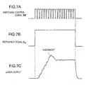
- this embodiment is capable of effecting a stable and rapid rise in the output of the pulsed laser beam LB and eliminating any overshoot.
- Such enhanced accuracy and stability of the laser output waveform control can lead to improved laser processing quality.
- Fig. 5 depicts a variant of the switching control unit 50 included in this embodiment.
- identical reference numerals are given to elements having similar configurations to those of Fig. 2.
- the reference signal S ref is passed through the inverting circuit 62 and thereafter added to sub-feedback signal SPc (SIc) by the adder 60 to obtain a first comparison error ⁇ S ref - SPc (SIc) ⁇ . That is, the inverting circuit 62 and the adder 60 make up a subtractor for subtracting the sub-feedback signal SPc (SIc) from the reference signal S ref .
- the first comparison error ⁇ S ref - SPc (SIc) ⁇ is fed to the inverting input terminal (-) of the operational amplifier 84 whilst the main feedback signal SL is fed to the non-inverting input terminal (+) to obtain a second comparison error ⁇ SL + SPc (SIc) - S ref ⁇ .
- the second comparison error is the same result as in the above embodiment, allowing the same error signal ER to be fed to the PWM circuit 66.
- the present invention may variously be changed or modified based on the technical idea thereof.
- the configurations and operative functions of the laser oscillation unit 10, laser power supply unit 12 and control unit 16 are not limited to those in the above embodiments, but instead may variously be altered.
- the above embodiment has employed the PWM as the switching control system, any other switching control system suited to the feedback loop is also available.
- the feedback signal (laser output measured value) or the reference value is corrected by the AC component of the power or the current supplied from the laser power supply unit to the excitation light source of the laser oscillation unit to provide a power feedback control, whereby it is possible to effect a stable and rapid-response laser power waveform control and especially to improve the rise characteristics of the laser output.
Landscapes
- Physics & Mathematics (AREA)
- Electromagnetism (AREA)
- Engineering & Computer Science (AREA)
- Plasma & Fusion (AREA)
- Optics & Photonics (AREA)
- Lasers (AREA)
- Laser Beam Processing (AREA)
Applications Claiming Priority (2)
| Application Number | Priority Date | Filing Date | Title |
|---|---|---|---|
| JP2000123591 | 2000-04-25 | ||
| JP2000123591A JP4520582B2 (ja) | 2000-04-25 | 2000-04-25 | レーザ加工装置 |
Publications (2)
| Publication Number | Publication Date |
|---|---|
| EP1150402A2 true EP1150402A2 (de) | 2001-10-31 |
| EP1150402A3 EP1150402A3 (de) | 2002-09-18 |
Family
ID=18633872
Family Applications (1)
| Application Number | Title | Priority Date | Filing Date |
|---|---|---|---|
| EP01303664A Withdrawn EP1150402A3 (de) | 2000-04-25 | 2001-04-20 | Laserbearbeitungsvorrichtung |
Country Status (5)
| Country | Link |
|---|---|
| US (1) | US20020012367A1 (de) |
| EP (1) | EP1150402A3 (de) |
| JP (1) | JP4520582B2 (de) |
| KR (1) | KR100774922B1 (de) |
| CN (1) | CN1320503A (de) |
Cited By (2)
| Publication number | Priority date | Publication date | Assignee | Title |
|---|---|---|---|---|
| US7250618B2 (en) | 2005-02-02 | 2007-07-31 | Nikon Corporation | Radiantly heated cathode for an electron gun and heating assembly |
| CN101966618A (zh) * | 2010-11-12 | 2011-02-09 | 深圳市华意隆实业发展有限公司 | 一种无电抗器无分流器电流型pwm逆变式焊割电源 |
Families Citing this family (19)
| Publication number | Priority date | Publication date | Assignee | Title |
|---|---|---|---|---|
| KR20030084408A (ko) * | 2002-04-26 | 2003-11-01 | 주식회사 이오테크닉스 | 레이저 마킹시스템의 파워보상방법 및 레이저 마킹시스템 |
| US7085296B2 (en) * | 2003-12-05 | 2006-08-01 | Branson Ultrasonics Corporation | Dual parameter laser optical feedback |
| US7363180B2 (en) * | 2005-02-15 | 2008-04-22 | Electro Scientific Industries, Inc. | Method for correcting systematic errors in a laser processing system |
| JP4846282B2 (ja) * | 2005-06-29 | 2011-12-28 | ミヤチテクノス株式会社 | 電子部品パッケージ封止方法及び装置 |
| JP5203573B2 (ja) * | 2006-03-23 | 2013-06-05 | ミヤチテクノス株式会社 | レーザ加工装置 |
| CN101242069B (zh) * | 2007-02-06 | 2011-08-03 | 深圳市大族激光科技股份有限公司 | 用于固体激光器的功率反馈控制系统及固体激光器 |
| CN100592376C (zh) * | 2007-04-06 | 2010-02-24 | 鸿富锦精密工业(深圳)有限公司 | 光源驱动装置 |
| KR100949152B1 (ko) * | 2007-11-23 | 2010-03-25 | 삼성코닝정밀유리 주식회사 | 유리 기판 레이저 절단 장치 |
| CN101582220B (zh) * | 2008-05-13 | 2013-04-17 | 北京中视中科光电技术有限公司 | 用于具有多个激光器的显示系统的控制装置和控制方法 |
| JP5354969B2 (ja) * | 2008-06-17 | 2013-11-27 | ミヤチテクノス株式会社 | ファイバレーザ加工方法及びファイバレーザ加工装置 |
| JP5303305B2 (ja) * | 2009-02-16 | 2013-10-02 | 東芝Itコントロールシステム株式会社 | レーザ制御装置 |
| CN102107332B (zh) * | 2009-12-23 | 2013-11-06 | 深圳市大族激光科技股份有限公司 | 一种激光打孔方法及系统 |
| CN102724789B (zh) * | 2011-03-30 | 2014-05-28 | 英飞特电子(杭州)股份有限公司 | 一种控制led光输出量恒定的电路和方法 |
| CN102790350A (zh) * | 2011-05-17 | 2012-11-21 | 深圳市通发激光设备有限公司 | 一种灯泵浦脉冲yag激光启动过程中能量补偿方法 |
| JP6362130B2 (ja) * | 2013-04-26 | 2018-07-25 | ビアメカニクス株式会社 | レーザ加工方法及びレーザ加工装置 |
| CN104360642B (zh) * | 2014-11-17 | 2018-04-27 | 大族激光科技产业集团股份有限公司 | 一种激光切割机数控系统 |
| JP6382901B2 (ja) * | 2016-09-29 | 2018-08-29 | ファナック株式会社 | レーザー加工システム |
| CN106502212B (zh) * | 2016-10-20 | 2020-05-19 | 大族激光科技产业集团股份有限公司 | 一种激光数控机床的集成数控系统 |
| CN107733409B (zh) * | 2017-10-27 | 2020-11-10 | 南京轨道交通系统工程有限公司 | 一种高压大功率igbt驱动电路 |
Citations (3)
| Publication number | Priority date | Publication date | Assignee | Title |
|---|---|---|---|---|
| EP0866529A2 (de) * | 1997-03-19 | 1998-09-23 | Miyachi Technos Corporation | Eine Lasermonitorvorrichtung und eine Laservorrichtung |
| EP0937534A2 (de) * | 1998-02-24 | 1999-08-25 | Miyachi Technos Corporation | Laserbearbeitungsvorrichtung |
| EP0958883A2 (de) * | 1998-05-18 | 1999-11-24 | Miyachi Technos Corporation | Laserbehandlungsvorrichtung |
Family Cites Families (5)
| Publication number | Priority date | Publication date | Assignee | Title |
|---|---|---|---|---|
| JPS6373681A (ja) * | 1986-09-17 | 1988-04-04 | Toshiba Corp | レ−ザ発振装置 |
| US4812641A (en) * | 1987-02-03 | 1989-03-14 | General Electric Company | High power optical fiber failure detection system |
| JP3373531B2 (ja) * | 1989-12-21 | 2003-02-04 | 株式会社東芝 | 半導体装置及び半導体レーザ装置 |
| JPH04345078A (ja) * | 1991-05-22 | 1992-12-01 | Sony Corp | レーザ光発生装置 |
| US5999549A (en) * | 1998-02-09 | 1999-12-07 | International Business Machines Corporation | Method and apparatus for laser safety |
-
2000
- 2000-04-25 JP JP2000123591A patent/JP4520582B2/ja not_active Expired - Lifetime
-
2001
- 2001-04-18 KR KR1020010020795A patent/KR100774922B1/ko active IP Right Grant
- 2001-04-20 EP EP01303664A patent/EP1150402A3/de not_active Withdrawn
- 2001-04-24 US US09/840,087 patent/US20020012367A1/en not_active Abandoned
- 2001-04-25 CN CN01117201A patent/CN1320503A/zh active Pending
Patent Citations (3)
| Publication number | Priority date | Publication date | Assignee | Title |
|---|---|---|---|---|
| EP0866529A2 (de) * | 1997-03-19 | 1998-09-23 | Miyachi Technos Corporation | Eine Lasermonitorvorrichtung und eine Laservorrichtung |
| EP0937534A2 (de) * | 1998-02-24 | 1999-08-25 | Miyachi Technos Corporation | Laserbearbeitungsvorrichtung |
| EP0958883A2 (de) * | 1998-05-18 | 1999-11-24 | Miyachi Technos Corporation | Laserbehandlungsvorrichtung |
Cited By (2)
| Publication number | Priority date | Publication date | Assignee | Title |
|---|---|---|---|---|
| US7250618B2 (en) | 2005-02-02 | 2007-07-31 | Nikon Corporation | Radiantly heated cathode for an electron gun and heating assembly |
| CN101966618A (zh) * | 2010-11-12 | 2011-02-09 | 深圳市华意隆实业发展有限公司 | 一种无电抗器无分流器电流型pwm逆变式焊割电源 |
Also Published As
| Publication number | Publication date |
|---|---|
| JP2001308428A (ja) | 2001-11-02 |
| KR100774922B1 (ko) | 2007-11-09 |
| EP1150402A3 (de) | 2002-09-18 |
| US20020012367A1 (en) | 2002-01-31 |
| KR20010098705A (ko) | 2001-11-08 |
| CN1320503A (zh) | 2001-11-07 |
| JP4520582B2 (ja) | 2010-08-04 |
Similar Documents
| Publication | Publication Date | Title |
|---|---|---|
| EP1150402A2 (de) | Laserbearbeitungsvorrichtung | |
| JPH0211272A (ja) | 負荷電圧検出システムと該検出システムを用いたパルスアーク溶接装置並びにパルスレーザ装置及び表面処理装置 | |
| US20020009105A1 (en) | Light emitting device | |
| JP4107532B2 (ja) | レーザ装置 | |
| US9203214B2 (en) | Laser system | |
| US4856012A (en) | Apparatus for controlling light output of a pulse-excited laser oscillator | |
| EP0705058A1 (de) | Gerät zur elektrische Stromversorgung einer Blitzlampe und geeignetes Verfahren | |
| KR102615048B1 (ko) | 레이저가공기 및 그 전원장치 | |
| JPS6244438B2 (de) | ||
| JP2009158344A (ja) | 重水素放電管用電源装置とその制御方法並びに分析装置 | |
| JP3496434B2 (ja) | レーザ用定電流電源装置及びレーザ加工装置 | |
| JP5303305B2 (ja) | レーザ制御装置 | |
| JPH07154013A (ja) | パルスレーザ装置 | |
| JPS62224485A (ja) | レ−ザ加工装置 | |
| JPH052316A (ja) | 半導体レーザの出力調整方法 | |
| JP2000340873A (ja) | 固体レーザ装置の光出力制御方法、固体レーザ装置及びレーザ電源装置 | |
| JPS60223180A (ja) | レ−ザ出力制御装置 | |
| JP2000349376A (ja) | レーザ発振器用電源装置 | |
| JP2989112B2 (ja) | レーザ溶接方法 | |
| JP3736117B2 (ja) | インバータ溶接機 | |
| JPS6398174A (ja) | 高周波放電励起レ−ザ装置 | |
| SU1445882A1 (ru) | Устройство питани дл дуговой сварки | |
| JPS63153875A (ja) | レーザ電源装置 | |
| SU1172097A1 (ru) | Рентгеновский аппарат | |
| JPH0738190A (ja) | 炭酸ガスレーザ発振装置の制御方法 |
Legal Events
| Date | Code | Title | Description |
|---|---|---|---|
| PUAI | Public reference made under article 153(3) epc to a published international application that has entered the european phase |
Free format text: ORIGINAL CODE: 0009012 |
|
| AK | Designated contracting states |
Kind code of ref document: A2 Designated state(s): AT BE CH CY DE DK ES FI FR GB GR IE IT LI LU MC NL PT SE TR |
|
| AX | Request for extension of the european patent |
Free format text: AL;LT;LV;MK;RO;SI |
|
| PUAL | Search report despatched |
Free format text: ORIGINAL CODE: 0009013 |
|
| AK | Designated contracting states |
Kind code of ref document: A3 Designated state(s): AT BE CH CY DE DK ES FI FR GB GR IE IT LI LU MC NL PT SE TR |
|
| AX | Request for extension of the european patent |
Free format text: AL;LT;LV;MK;RO;SI |
|
| AKX | Designation fees paid |
Designated state(s): DE FR GB IT NL |
|
| STAA | Information on the status of an ep patent application or granted ep patent |
Free format text: STATUS: THE APPLICATION IS DEEMED TO BE WITHDRAWN |
|
| 18D | Application deemed to be withdrawn |
Effective date: 20030319 |