EP1148634A2 - Verstärkerschaltung - Google Patents
Verstärkerschaltung Download PDFInfo
- Publication number
- EP1148634A2 EP1148634A2 EP01100365A EP01100365A EP1148634A2 EP 1148634 A2 EP1148634 A2 EP 1148634A2 EP 01100365 A EP01100365 A EP 01100365A EP 01100365 A EP01100365 A EP 01100365A EP 1148634 A2 EP1148634 A2 EP 1148634A2
- Authority
- EP
- European Patent Office
- Prior art keywords
- transistor
- amplifier
- amplifier circuit
- circuit according
- input
- Prior art date
- Legal status (The legal status is an assumption and is not a legal conclusion. Google has not performed a legal analysis and makes no representation as to the accuracy of the status listed.)
- Granted
Links
Images
Classifications
-
- H—ELECTRICITY
- H03—ELECTRONIC CIRCUITRY
- H03F—AMPLIFIERS
- H03F1/00—Details of amplifiers with only discharge tubes, only semiconductor devices or only unspecified devices as amplifying elements
- H03F1/30—Modifications of amplifiers to reduce influence of variations of temperature or supply voltage or other physical parameters
- H03F1/301—Modifications of amplifiers to reduce influence of variations of temperature or supply voltage or other physical parameters in MOSFET amplifiers
Definitions
- the invention relates to a high-frequency amplifier circuit with regulation by working point setting.
- the characteristic curve of a power amplifier depends on the characteristic curve of the internal transistors.
- the positioning characteristic of the power amplifier depends, for example, on the threshold voltage U TO of the field-effect transistors.
- the threshold voltage U TO of the field effect transistors like their steepness, is dependent on manufacturing tolerances. In the case of small dimensions, the threshold voltage depends, for example, on the channel length and channel width of the field effect transistor.
- High frequency power amplifiers are found, for example, as Transmitter amplifiers in systems using the time slot method (Time Division Multiple Access, TDMA procedure) work.
- An example of such a time slot method is the cellular standard GSM.
- the procedure is the sending of data in so-called time slices disassembled. So in a state of rest of the high frequency amplifier the output power of the same is zero, one must amplifier controlling the amplifier at the control input of the High frequency amplifier a voltage below the threshold voltage of the amplifier transistor. Hereby but is the characteristic of the high frequency amplifier in adversely affected. From the resting tension of the Regulator, which is present at the input of the amplifier, up to Power input of the amplifier at the beginning of a transmission time slot there is a dead zone, which the control properties of the system worsened.
- control properties of the system become too bad, it must a comparison can be made.
- This comparison is known individually, for example with a potentiometer, or to modify the target voltage of the regulator, for example by overlaying an offset. Realizations however, these individual comparison options are very good complex.
- a need for adjustment when controlling a power amplifier can also be caused by changing environmental conditions, for example temperature, or by changing the supply voltage be given.
- the object of the present invention is an amplifier circuit to be stated with compensation for manufacturing-related tolerances.
- an amplifier circuit comprising a power amplifier with a first transistor to which a supply voltage can be supplied is an input signal can be fed to its control input and an output signal can be derived at its first load connection is a control amplifier with an operational amplifier, its output with the control input of the first Transistor is connected, and its first input to the first load terminal of the first transistor is connected, and a reference stage with a second transistor, to which the supply voltage can be fed, and that to the operational amplifier is connected so that this is a reference voltage is feedable.
- a first transistor is specified as the power amplifier, which can be connected to a supply voltage.
- This amplifier becomes an input signal to be amplified on the input side fed, and on the output side is as an output signal the amplified input signal can be tapped.
- This power amplifier is controlled by a control amplifier.
- the control amplifier has an operational amplifier, the Output is connected to the input of the first transistor.
- the output signal that can be tapped at the amplifier is on fed back a first input of the operational amplifier.
- the power amplifier provides information on this regulator arrangement represents the actuator.
- To form a reference voltage a second transistor is provided in a reference stage, which with the operational amplifier to transmit a Reference voltage value is connected. This second transistor is a physical image of the first transistor, so that it can be used for tolerance compensation.
- First one and second transistor are of the same transistor type, however, the second transistor is opposite the first transistor scaled.
- the first and the second transistor have in particular the same electrical conditions.
- On one second input of the operational amplifier is through a filter a target signal of the controller can be supplied, which the desired Output power of the power amplifier indicates.
- the Indian Reference stage arranged second transistor forms with the Control amplifier a compensation circuit for the high-frequency power amplifier, so that the scheme is adjustment-free can work.
- the present circuit the additional advantage that the Temperature and operating voltage dependency of the amplifier circuit co-recorded by the reference level and automatically is compensated. Such a change in temperature can, for example be operational or due to external influences arise.
- the circuit when using the circuit as a transmitter amplifier in the mobile radio area, for example, the operating voltage depends of the state of charge of an accumulator of the mobile radio device from.
- the power amplifier and the reference stage are the power amplifier and the reference stage arranged on the same semiconductor device.
- a good pairing of the transistors during production ensures that the first and the second transistor Have characteristic values that differ as little as possible and on the other hand the arrangement is based on the same chip enables close thermal coupling.
- Threshold voltage of the first transistor thereby from the control amplifier that the second transistor, which is arranged in the reference stage, at its source connection has a high resistance to ground, above which the threshold voltage practically drops.
- This Reference voltage is via a connection between reference level and operational amplifier to compensate for the tolerances the threshold voltage of the first transistor is used.
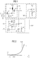
- FIG. 1 shows a basic circuit arrangement with a high-frequency amplifier PA, such as is used, for example, as a transmitter amplifier in the mobile radio sector.
- the signal-amplifying transistor T1 is designed as a field-effect transistor. This can be connected to a voltage source V CC via a coil L1 for high-frequency decoupling.
- An input signal E to be amplified can be fed to the gate of the transistor, decoupled via a first capacitor C1.
- the amplified signal can be tapped at the output of the transistor as output signal A, again decoupled via a capacitor C2, and fed to a consumer, for example a transmitting antenna.
- a control signal can also be fed to the control input of the field-effect transistor T1 via a resistor R1, which control signal serves for the power specification of the high-frequency amplifier by the controller CU.
- This power specification is carried out essentially by setting the operating point of the field effect transistor T1.
- the control amplifier CU has an operational amplifier OP, at the output of which the control signal for the high-frequency amplifier PA can be tapped.
- a setpoint signal can be fed to the operational amplifier OP, which contains the power specification for the high-frequency amplifier PA. In the present example, this setpoint signal can be fed to the minus input OP2 of the operational amplifier OP, to which a feedback branch, which can have an integrating capacitor C3, can also be connected.
- the output signal A of the high-frequency amplifier PA is connected to the plus input OP1 of the operational amplifier OP via a diode D1.
- a capacitor C4 and, in parallel, a resistor R2 for realizing a low pass to ground are also connected between diode D1 and operational amplifier input OP1.
- the power signal which can be tapped at the output of the high-frequency amplifier is converted into a voltage value to be processed by the operational amplifier.
- a reference stage is arranged, which has a second transistor T2. With its transistor T2, this reference stage has a physical image of the transistor T1.
- Transistor T2 is of the same type as transistor T1, but is scaled. In particular, the transistor T2 has the same electrical DC ratios as the transistor T1.
- the present exemplary embodiment serves to compensate for tolerances with regard to the threshold voltage of field-effect transistor T1.
- the source connection of the reference transistor T2 has a resistor R3 connected to ground, via which, when the resistor R3 is chosen to have a high resistance, the threshold voltage U TO almost drops.
- This reference voltage UREF is fed to the operational amplifier OP via a line and is used there to adjust the tolerances.
- the controller CU is made of silicon realized, and power amplifier PA and reference stage REF both in either GaAs technology or in HBT (hetero bipolar transistor) technology.
- FIG. 2 shows the transfer characteristic of a field effect transistor T2, namely the drain current I D as a function of the gate-source voltage U GS .
- the resistance characteristic of the reference resistor R3 is also shown. The intersection of both characteristics leads to the tapped reference voltage UREF. It can be seen that the reference voltage UREF that can be derived from the circuit corresponds more precisely to the threshold voltage U TO of the field-effect transistor T2, the higher the resistance R3 is chosen.
- Arranging transistor provides particular advantages T1 and transistor T2 on the same chip because of a good pairing and good thermal coupling can be achieved. This is with the dashed line in Figure 1 around power amplifier PA and reference level REF indicated.
- the reference voltage UREF could also be in a reference circuit generated with the resistor R3 is replaced by a constant current source. Besides, could the current, instead of on the source side also on the drain side using additional control amplifiers.
- the current flowing in the reference stage does not necessarily have to be very small, because even with higher currents a good correlation of the reference voltage UREF with the Threshold voltage exists.
- a voltage signal UREF for referencing too a current can be used as a reference in which, for example the reference resistor R3 itself part of the inverting Part of the operational amplifier OP for generation of a quiet signal.
- the transistors T1, T2 could also be bipolar transistors his.
- the compensation could manufacturing-related tolerances on the direct current gain B or the small signal gain ß Respectively.
Landscapes
- Engineering & Computer Science (AREA)
- Power Engineering (AREA)
- Amplifiers (AREA)
Abstract
Description
- Figur 1
- Ein Ausführungsbeispiel der vorliegenden Erfindung anhand eines vereinfachten Schaltbilds,
- Figur 2
- Die Arbeitspunkt-Einstellung der Referenzstufe.
Claims (9)
- Verstärkerschaltung, welche umfaßt:einen Leistungsverstärker (PA) mit einem ersten Transistor (T1), dem eine Versorgungsspannung (VCC) zuführbar ist, dem an seinem Steuereingang ein Eingangssignal (E) zuführbar ist, und an dessen erstem Lastanschluß ein Ausgangssignal (A) ableitbar ist,einen Regelverstärker (CU) mit einem Operationsverstärker (OP), dessen Ausgang mit dem Steuereingang des ersten Transistors (T1) verbunden ist, und dessen erster Eingang (OP1) mit dem ersten Lastanschluß des ersten Transistors (T1) verbunden ist, undeine Referenzstufe (REF) mit einem zweiten Transistor (T2), dem die Versorgungsspannung (VCC) zuführbar ist, und der an den Operationsverstärker (OP) angeschlossen ist, so daß diesem eine Referenzspannung (UREF) zuführbar ist.
- Verstärkerschaltung nach Anspruch 1,
dadurch gekennzeichnet, daß
erster und zweiter Transistor (T1, T2) auf dem gleichen Chip angeordnet sind. - Verstärkerschaltung nach Anspruch 1 oder 2,
dadurch gekennzeichnet, daß
das Eingangssignal (E) mittels eines an den Steuereingang des ersten Transistors (T1) angeschlossenen Kondensators (C1) zuführbar und das Ausgangssignal (A) mittels eines an den ersten Lastanschluß des ersten Transistors (T1) angeschlossenen Kondensators (C2) ableitbar ist. - Verstärkerschaltung nach einem der Ansprüche 1 bis 3,
dadurch gekennzeichnet, daß
ein Kondensator (C3) zwischen Ausgang und zweitem Eingang (OP2) des Operationsverstärkers (OP) geschaltet ist. - Verstärkerschaltung nach einem der Ansprüche 1 bis 4,
dadurch gekennzeichnet, daß
der erste und zweite Transistor (T1, T2) Feldeffekt-Transistoren gleichen Typs sind. - Verstärkerschaltung nach Anspruch 5,
dadurch gekennzeichnet, daß
der erste und der zweite Transistor (T1, T2) gleiche Steilheit und gleiche Schwellenspannung UTO aufweisen. - Verstärkerschaltung nach Anspruch 6,
dadurch gekennzeichnet, daß
der Referenz-Widerstand (R3) hochohmig ist. - Verstärkerschaltung nach einem der Ansprüche 1 bis 4,
dadurch gekennzeichnet, daß
der erste und der zweite Transistor (T1, T2) Bipolar-Transistoren gleichen Typs sind. - Verstärkerschaltung nach Anspruch 8,
dadurch gekennzeichnet, daß
der erste und zweite Transistor (T1, T2) gleiche statische Stromverstärkung und gleiche differentielle Stromverstärkung haben.
Applications Claiming Priority (2)
| Application Number | Priority Date | Filing Date | Title |
|---|---|---|---|
| DE10002371A DE10002371A1 (de) | 2000-01-20 | 2000-01-20 | Verstärkerschaltung |
| DE10002371 | 2000-01-20 |
Publications (3)
| Publication Number | Publication Date |
|---|---|
| EP1148634A2 true EP1148634A2 (de) | 2001-10-24 |
| EP1148634A3 EP1148634A3 (de) | 2004-01-14 |
| EP1148634B1 EP1148634B1 (de) | 2006-10-04 |
Family
ID=7628178
Family Applications (1)
| Application Number | Title | Priority Date | Filing Date |
|---|---|---|---|
| EP01100365A Expired - Lifetime EP1148634B1 (de) | 2000-01-20 | 2001-01-05 | Verstärkerschaltung |
Country Status (3)
| Country | Link |
|---|---|
| US (1) | US6535059B2 (de) |
| EP (1) | EP1148634B1 (de) |
| DE (2) | DE10002371A1 (de) |
Families Citing this family (3)
| Publication number | Priority date | Publication date | Assignee | Title |
|---|---|---|---|---|
| US7088175B2 (en) * | 2001-02-13 | 2006-08-08 | Quantum Applied Science & Research, Inc. | Low noise, electric field sensor |
| US6768369B1 (en) * | 2003-05-30 | 2004-07-27 | Intel Corporation | Threshold voltage compensation |
| US7728671B2 (en) * | 2008-01-17 | 2010-06-01 | Infineon Technologies Ag | Semiconductor power device with bias circuit |
Family Cites Families (10)
| Publication number | Priority date | Publication date | Assignee | Title |
|---|---|---|---|---|
| DE3141790A1 (de) * | 1981-10-21 | 1983-04-28 | Siemens AG, 1000 Berlin und 8000 München | Integrierbare frequenzteilerschaltung |
| JP3113401B2 (ja) * | 1992-07-31 | 2000-11-27 | リーダー電子株式会社 | 広帯域増幅器 |
| US5394113A (en) * | 1992-08-28 | 1995-02-28 | Harris Corporation | High impedance low-distortion linear amplifier |
| US5986508A (en) * | 1996-08-26 | 1999-11-16 | Nevin; Larry J. | Bias concept for intrinsic gain stabilization over temperature |
| DE19732437C1 (de) * | 1997-07-28 | 1998-12-24 | Siemens Ag | Transistor-Verstärkerstufe |
| US5854578A (en) * | 1997-09-15 | 1998-12-29 | Motorola, Inc. | Active circuit having a temperature stable bias |
| DE19742954C1 (de) * | 1997-09-29 | 1999-02-25 | Fraunhofer Ges Forschung | Temperaturkompensationsschaltung für Feldeffekttransistor-Verstärkerschaltungen |
| DE19811839A1 (de) * | 1998-03-18 | 1999-09-23 | Siemens Ag | Schaltungsanordnung zur Steuerung der Ausgangsleistung einer Verstärkereinrichtung |
| DE19827702C2 (de) * | 1998-06-22 | 2000-06-08 | Siemens Ag | Verstärkerschaltung mit aktiver Arbeitspunkteinstellung |
| US6323730B1 (en) * | 1999-04-30 | 2001-11-27 | Pcb Piezotronics, Inc. | High resolution zero input current charge sensitive preamplifier |
-
2000
- 2000-01-20 DE DE10002371A patent/DE10002371A1/de not_active Withdrawn
-
2001
- 2001-01-05 EP EP01100365A patent/EP1148634B1/de not_active Expired - Lifetime
- 2001-01-05 DE DE50111123T patent/DE50111123D1/de not_active Expired - Lifetime
- 2001-01-22 US US09/767,802 patent/US6535059B2/en not_active Expired - Lifetime
Also Published As
| Publication number | Publication date |
|---|---|
| US6535059B2 (en) | 2003-03-18 |
| US20010009388A1 (en) | 2001-07-26 |
| DE50111123D1 (de) | 2006-11-16 |
| EP1148634A3 (de) | 2004-01-14 |
| EP1148634B1 (de) | 2006-10-04 |
| DE10002371A1 (de) | 2001-08-09 |
Similar Documents
| Publication | Publication Date | Title |
|---|---|---|
| DE69427311T2 (de) | Vorspannungsstabilisierungsschaltung | |
| DE10000224B4 (de) | Leistungsverstärker mit einer Schutzschaltung | |
| DE102013109363B4 (de) | Chipkarte | |
| DE69718301T2 (de) | Linearer hochfrequenzverstärker mit hoher eingangsimpedanz und hohem leistungswirkungsgrad | |
| EP1004165B1 (de) | Aktive arbeitspunkteeinstellung für leistungsverstärker | |
| DE102008022950B4 (de) | Verstärkeranordnung mit mehreren Betriebsarten und Verfahren zum Steuern einer Verstärkeranordnung | |
| DE10393755T5 (de) | Schaltung zur aktiven Self-Bias-Kompensation für einen Hochfrequenzleistungsverstärker | |
| EP1264396B1 (de) | Schaltungsanordnung zur arbeitspunkteinstellung eines hochfrequenztransistors und verstärkerschaltung | |
| DE2250625B2 (de) | Schaltungsanordnung zur Konstanthaltung eines an eine Last gelieferten Stromes | |
| DE102005007876A1 (de) | Verstärkerschaltung mit reduzierter Temperaturabhängingkeit der Verstärkung | |
| EP1101279B1 (de) | Verstärkerausgangsstufe | |
| EP1148634B1 (de) | Verstärkerschaltung | |
| DE69117032T2 (de) | Endstufe mit dem Verstärkungsfaktor Eins insbesondere für monolithisch integrierbare Leistungsverstärker | |
| EP0499657A1 (de) | Integrierbarer Shunt-Regler | |
| DE19521663A1 (de) | Integrierter Schaltkreis mit Spannungsregelschaltung | |
| EP1402328B1 (de) | Stromquellenschaltung | |
| DE102010032574A1 (de) | Schaltungsanordnung zur Erzeugung von Mikrowellen-Schwingungen | |
| EP0289807B1 (de) | Verfahren zur Temperaturkompensation von elektrischen Netzwerken sowie Anordnungen hierzu | |
| EP0277377A1 (de) | Schaltungsanordnung zur Bildung eines begrenzten Stromes | |
| EP0990199B1 (de) | Reglervorrichtung | |
| EP0792014A2 (de) | Anordnung zur Regelung der Ausgangsamplitude eines Hochfrequenz-Leistungsverstärkers | |
| DE102007026297A1 (de) | Dämpfungsglied | |
| DE2657729C2 (de) | Gegengekoppelter Breitbandverstärker | |
| DE10231156B4 (de) | Schaltung zum Liefern einer Basis-Betriebsspannung für einen Bipolartransistor und Verstärkerschaltung | |
| DE3224475A1 (de) | Elektronischer verstaerker |
Legal Events
| Date | Code | Title | Description |
|---|---|---|---|
| PUAI | Public reference made under article 153(3) epc to a published international application that has entered the european phase |
Free format text: ORIGINAL CODE: 0009012 |
|
| AK | Designated contracting states |
Kind code of ref document: A2 Designated state(s): AT BE CH CY DE DK ES FI FR GB GR IE IT LI LU MC NL PT SE TR |
|
| AX | Request for extension of the european patent |
Free format text: AL;LT;LV;MK;RO;SI |
|
| PUAL | Search report despatched |
Free format text: ORIGINAL CODE: 0009013 |
|
| AK | Designated contracting states |
Kind code of ref document: A3 Designated state(s): AT BE CH CY DE DK ES FI FR GB GR IE IT LI LU MC NL PT SE TR |
|
| AX | Request for extension of the european patent |
Extension state: AL LT LV MK RO SI |
|
| 17P | Request for examination filed |
Effective date: 20040630 |
|
| AKX | Designation fees paid |
Designated state(s): DE FR GB |
|
| GRAP | Despatch of communication of intention to grant a patent |
Free format text: ORIGINAL CODE: EPIDOSNIGR1 |
|
| GRAS | Grant fee paid |
Free format text: ORIGINAL CODE: EPIDOSNIGR3 |
|
| GRAA | (expected) grant |
Free format text: ORIGINAL CODE: 0009210 |
|
| AK | Designated contracting states |
Kind code of ref document: B1 Designated state(s): DE FR GB |
|
| REG | Reference to a national code |
Ref country code: GB Ref legal event code: FG4D Free format text: NOT ENGLISH |
|
| REF | Corresponds to: |
Ref document number: 50111123 Country of ref document: DE Date of ref document: 20061116 Kind code of ref document: P |
|
| GBT | Gb: translation of ep patent filed (gb section 77(6)(a)/1977) |
Effective date: 20070103 |
|
| ET | Fr: translation filed | ||
| PLBE | No opposition filed within time limit |
Free format text: ORIGINAL CODE: 0009261 |
|
| STAA | Information on the status of an ep patent application or granted ep patent |
Free format text: STATUS: NO OPPOSITION FILED WITHIN TIME LIMIT |
|
| 26N | No opposition filed |
Effective date: 20070705 |
|
| REG | Reference to a national code |
Ref country code: FR Ref legal event code: TP Owner name: INTEL MOBILE COMMUNICATIONS GMBH, DE Effective date: 20120404 Ref country code: FR Ref legal event code: CA Effective date: 20120404 |
|
| REG | Reference to a national code |
Ref country code: GB Ref legal event code: 732E Free format text: REGISTERED BETWEEN 20120607 AND 20120613 |
|
| REG | Reference to a national code |
Ref country code: GB Ref legal event code: 732E Free format text: REGISTERED BETWEEN 20121213 AND 20121219 |
|
| REG | Reference to a national code |
Ref country code: DE Ref legal event code: R081 Ref document number: 50111123 Country of ref document: DE Owner name: INTEL MOBILE COMMUNICATIONS GMBH, DE Free format text: FORMER OWNER: INTEL MOBILE COMMUNICATIONS GMBH, 85579 NEUBIBERG, DE Effective date: 20130315 Ref country code: DE Ref legal event code: R081 Ref document number: 50111123 Country of ref document: DE Owner name: INTEL MOBILE COMMUNICATIONS GMBH, DE Free format text: FORMER OWNER: INTEL MOBILE COMMUNICATIONS TECHNOLOGY GMBH, 85579 NEUBIBERG, DE Effective date: 20130326 Ref country code: DE Ref legal event code: R081 Ref document number: 50111123 Country of ref document: DE Owner name: INTEL MOBILE COMMUNICATIONS GMBH, DE Free format text: FORMER OWNER: INFINEON TECHNOLOGIES AG, 81669 MUENCHEN, DE Effective date: 20130314 Ref country code: DE Ref legal event code: R081 Ref document number: 50111123 Country of ref document: DE Owner name: INTEL MOBILE COMMUNICATIONS GMBH, DE Free format text: FORMER OWNER: INFINEON TECHNOLOGIES AG, 85579 NEUBIBERG, DE Effective date: 20130315 |
|
| REG | Reference to a national code |
Ref country code: FR Ref legal event code: PLFP Year of fee payment: 15 |
|
| PGFP | Annual fee paid to national office [announced via postgrant information from national office to epo] |
Ref country code: GB Payment date: 20141231 Year of fee payment: 15 |
|
| PGFP | Annual fee paid to national office [announced via postgrant information from national office to epo] |
Ref country code: FR Payment date: 20150108 Year of fee payment: 15 |
|
| REG | Reference to a national code |
Ref country code: FR Ref legal event code: CD Owner name: INTEL DEUTSCHLAND GMBH, DE Effective date: 20160126 |
|
| PGFP | Annual fee paid to national office [announced via postgrant information from national office to epo] |
Ref country code: DE Payment date: 20151229 Year of fee payment: 16 |
|
| GBPC | Gb: european patent ceased through non-payment of renewal fee |
Effective date: 20160105 |
|
| REG | Reference to a national code |
Ref country code: FR Ref legal event code: ST Effective date: 20160930 |
|
| PG25 | Lapsed in a contracting state [announced via postgrant information from national office to epo] |
Ref country code: GB Free format text: LAPSE BECAUSE OF NON-PAYMENT OF DUE FEES Effective date: 20160105 |
|
| PG25 | Lapsed in a contracting state [announced via postgrant information from national office to epo] |
Ref country code: FR Free format text: LAPSE BECAUSE OF NON-PAYMENT OF DUE FEES Effective date: 20160201 |
|
| REG | Reference to a national code |
Ref country code: DE Ref legal event code: R119 Ref document number: 50111123 Country of ref document: DE |
|
| PG25 | Lapsed in a contracting state [announced via postgrant information from national office to epo] |
Ref country code: DE Free format text: LAPSE BECAUSE OF NON-PAYMENT OF DUE FEES Effective date: 20170801 |