EP1146574A2 - Organic luminescence device and process for production thereof - Google Patents
Organic luminescence device and process for production thereof Download PDFInfo
- Publication number
- EP1146574A2 EP1146574A2 EP01109143A EP01109143A EP1146574A2 EP 1146574 A2 EP1146574 A2 EP 1146574A2 EP 01109143 A EP01109143 A EP 01109143A EP 01109143 A EP01109143 A EP 01109143A EP 1146574 A2 EP1146574 A2 EP 1146574A2
- Authority
- EP
- European Patent Office
- Prior art keywords
- organic
- film
- luminescence device
- double bonds
- polymerizable double
- Prior art date
- Legal status (The legal status is an assumption and is not a legal conclusion. Google has not performed a legal analysis and makes no representation as to the accuracy of the status listed.)
- Granted
Links
- 0 CC1*=*(C)C=C1 Chemical compound CC1*=*(C)C=C1 0.000 description 4
Images

Classifications
-
- H—ELECTRICITY
- H10—SEMICONDUCTOR DEVICES; ELECTRIC SOLID-STATE DEVICES NOT OTHERWISE PROVIDED FOR
- H10K—ORGANIC ELECTRIC SOLID-STATE DEVICES
- H10K85/00—Organic materials used in the body or electrodes of devices covered by this subclass
- H10K85/10—Organic polymers or oligomers
- H10K85/111—Organic polymers or oligomers comprising aromatic, heteroaromatic, or aryl chains, e.g. polyaniline, polyphenylene or polyphenylene vinylene
-
- C—CHEMISTRY; METALLURGY
- C09—DYES; PAINTS; POLISHES; NATURAL RESINS; ADHESIVES; COMPOSITIONS NOT OTHERWISE PROVIDED FOR; APPLICATIONS OF MATERIALS NOT OTHERWISE PROVIDED FOR
- C09K—MATERIALS FOR MISCELLANEOUS APPLICATIONS, NOT PROVIDED FOR ELSEWHERE
- C09K11/00—Luminescent materials, e.g. electroluminescent or chemiluminescent
- C09K11/06—Luminescent materials, e.g. electroluminescent or chemiluminescent containing organic luminescent materials
-
- H—ELECTRICITY
- H10—SEMICONDUCTOR DEVICES; ELECTRIC SOLID-STATE DEVICES NOT OTHERWISE PROVIDED FOR
- H10K—ORGANIC ELECTRIC SOLID-STATE DEVICES
- H10K85/00—Organic materials used in the body or electrodes of devices covered by this subclass
- H10K85/10—Organic polymers or oligomers
- H10K85/141—Organic polymers or oligomers comprising aliphatic or olefinic chains, e.g. poly N-vinylcarbazol, PVC or PTFE
-
- H—ELECTRICITY
- H10—SEMICONDUCTOR DEVICES; ELECTRIC SOLID-STATE DEVICES NOT OTHERWISE PROVIDED FOR
- H10K—ORGANIC ELECTRIC SOLID-STATE DEVICES
- H10K2102/00—Constructional details relating to the organic devices covered by this subclass
- H10K2102/10—Transparent electrodes, e.g. using graphene
- H10K2102/101—Transparent electrodes, e.g. using graphene comprising transparent conductive oxides [TCO]
- H10K2102/103—Transparent electrodes, e.g. using graphene comprising transparent conductive oxides [TCO] comprising indium oxides, e.g. ITO
-
- H—ELECTRICITY
- H10—SEMICONDUCTOR DEVICES; ELECTRIC SOLID-STATE DEVICES NOT OTHERWISE PROVIDED FOR
- H10K—ORGANIC ELECTRIC SOLID-STATE DEVICES
- H10K85/00—Organic materials used in the body or electrodes of devices covered by this subclass
- H10K85/10—Organic polymers or oligomers
- H10K85/111—Organic polymers or oligomers comprising aromatic, heteroaromatic, or aryl chains, e.g. polyaniline, polyphenylene or polyphenylene vinylene
- H10K85/114—Poly-phenylenevinylene; Derivatives thereof
-
- H—ELECTRICITY
- H10—SEMICONDUCTOR DEVICES; ELECTRIC SOLID-STATE DEVICES NOT OTHERWISE PROVIDED FOR
- H10K—ORGANIC ELECTRIC SOLID-STATE DEVICES
- H10K85/00—Organic materials used in the body or electrodes of devices covered by this subclass
- H10K85/10—Organic polymers or oligomers
- H10K85/151—Copolymers
-
- H—ELECTRICITY
- H10—SEMICONDUCTOR DEVICES; ELECTRIC SOLID-STATE DEVICES NOT OTHERWISE PROVIDED FOR
- H10K—ORGANIC ELECTRIC SOLID-STATE DEVICES
- H10K85/00—Organic materials used in the body or electrodes of devices covered by this subclass
- H10K85/30—Coordination compounds
- H10K85/321—Metal complexes comprising a group IIIA element, e.g. Tris (8-hydroxyquinoline) gallium [Gaq3]
- H10K85/324—Metal complexes comprising a group IIIA element, e.g. Tris (8-hydroxyquinoline) gallium [Gaq3] comprising aluminium, e.g. Alq3
-
- H—ELECTRICITY
- H10—SEMICONDUCTOR DEVICES; ELECTRIC SOLID-STATE DEVICES NOT OTHERWISE PROVIDED FOR
- H10K—ORGANIC ELECTRIC SOLID-STATE DEVICES
- H10K85/00—Organic materials used in the body or electrodes of devices covered by this subclass
- H10K85/60—Organic compounds having low molecular weight
- H10K85/615—Polycyclic condensed aromatic hydrocarbons, e.g. anthracene
- H10K85/621—Aromatic anhydride or imide compounds, e.g. perylene tetra-carboxylic dianhydride or perylene tetracarboxylic di-imide
-
- H—ELECTRICITY
- H10—SEMICONDUCTOR DEVICES; ELECTRIC SOLID-STATE DEVICES NOT OTHERWISE PROVIDED FOR
- H10K—ORGANIC ELECTRIC SOLID-STATE DEVICES
- H10K85/00—Organic materials used in the body or electrodes of devices covered by this subclass
- H10K85/60—Organic compounds having low molecular weight
- H10K85/615—Polycyclic condensed aromatic hydrocarbons, e.g. anthracene
- H10K85/622—Polycyclic condensed aromatic hydrocarbons, e.g. anthracene containing four rings, e.g. pyrene
-
- H—ELECTRICITY
- H10—SEMICONDUCTOR DEVICES; ELECTRIC SOLID-STATE DEVICES NOT OTHERWISE PROVIDED FOR
- H10K—ORGANIC ELECTRIC SOLID-STATE DEVICES
- H10K85/00—Organic materials used in the body or electrodes of devices covered by this subclass
- H10K85/60—Organic compounds having low molecular weight
- H10K85/631—Amine compounds having at least two aryl rest on at least one amine-nitrogen atom, e.g. triphenylamine
-
- H—ELECTRICITY
- H10—SEMICONDUCTOR DEVICES; ELECTRIC SOLID-STATE DEVICES NOT OTHERWISE PROVIDED FOR
- H10K—ORGANIC ELECTRIC SOLID-STATE DEVICES
- H10K85/00—Organic materials used in the body or electrodes of devices covered by this subclass
- H10K85/60—Organic compounds having low molecular weight
- H10K85/649—Aromatic compounds comprising a hetero atom
- H10K85/656—Aromatic compounds comprising a hetero atom comprising two or more different heteroatoms per ring
- H10K85/6565—Oxadiazole compounds
-
- H—ELECTRICITY
- H10—SEMICONDUCTOR DEVICES; ELECTRIC SOLID-STATE DEVICES NOT OTHERWISE PROVIDED FOR
- H10K—ORGANIC ELECTRIC SOLID-STATE DEVICES
- H10K85/00—Organic materials used in the body or electrodes of devices covered by this subclass
- H10K85/60—Organic compounds having low molecular weight
- H10K85/649—Aromatic compounds comprising a hetero atom
- H10K85/657—Polycyclic condensed heteroaromatic hydrocarbons
-
- Y—GENERAL TAGGING OF NEW TECHNOLOGICAL DEVELOPMENTS; GENERAL TAGGING OF CROSS-SECTIONAL TECHNOLOGIES SPANNING OVER SEVERAL SECTIONS OF THE IPC; TECHNICAL SUBJECTS COVERED BY FORMER USPC CROSS-REFERENCE ART COLLECTIONS [XRACs] AND DIGESTS
- Y10—TECHNICAL SUBJECTS COVERED BY FORMER USPC
- Y10T—TECHNICAL SUBJECTS COVERED BY FORMER US CLASSIFICATION
- Y10T428/00—Stock material or miscellaneous articles
- Y10T428/31504—Composite [nonstructural laminate]
- Y10T428/31855—Of addition polymer from unsaturated monomers
-
- Y—GENERAL TAGGING OF NEW TECHNOLOGICAL DEVELOPMENTS; GENERAL TAGGING OF CROSS-SECTIONAL TECHNOLOGIES SPANNING OVER SEVERAL SECTIONS OF THE IPC; TECHNICAL SUBJECTS COVERED BY FORMER USPC CROSS-REFERENCE ART COLLECTIONS [XRACs] AND DIGESTS
- Y10—TECHNICAL SUBJECTS COVERED BY FORMER USPC
- Y10T—TECHNICAL SUBJECTS COVERED BY FORMER US CLASSIFICATION
- Y10T428/00—Stock material or miscellaneous articles
- Y10T428/31504—Composite [nonstructural laminate]
- Y10T428/31855—Of addition polymer from unsaturated monomers
- Y10T428/31909—Next to second addition polymer from unsaturated monomers
-
- Y—GENERAL TAGGING OF NEW TECHNOLOGICAL DEVELOPMENTS; GENERAL TAGGING OF CROSS-SECTIONAL TECHNOLOGIES SPANNING OVER SEVERAL SECTIONS OF THE IPC; TECHNICAL SUBJECTS COVERED BY FORMER USPC CROSS-REFERENCE ART COLLECTIONS [XRACs] AND DIGESTS
- Y10—TECHNICAL SUBJECTS COVERED BY FORMER USPC
- Y10T—TECHNICAL SUBJECTS COVERED BY FORMER US CLASSIFICATION
- Y10T428/00—Stock material or miscellaneous articles
- Y10T428/31504—Composite [nonstructural laminate]
- Y10T428/31855—Of addition polymer from unsaturated monomers
- Y10T428/31931—Polyene monomer-containing
Definitions
- the present invention relates to an organic (electro-)luminescence device having a film of organic compound capable of light emission under application of an electric field, and a process for production thereof.
- An organic luminescence device generally comprises a pair of electrodes (comprising an anode and a cathode) and a film comprising a fluorescent organic compound disposed between the electrodes.
- a pair of electrodes comprising an anode and a cathode
- a film comprising a fluorescent organic compound disposed between the electrodes.
- holes and electrons are injected from the anode and the cathode, respectively, thus forming excitons of the fluorescent organic compound.
- the organic luminescence device emits light or causes luminescence.
- an organic luminescence device using a conjugated polymer has been reported by a research group of Cambridge University ("Nature", vol. 347, pp. 539- (1990)). According to this report, a single layer of polyphenylenevinylene (PPV) is formed through a wet-coating process and luminescence from the single layer is confirmed.
- PSV polyphenylenevinylene
- Such an organic luminescence device using a conjugated polymer has also been proposed by, e.g., U.S. Patent Nos. 5,247,190, 5,514,878 and 5,672,678, JP-A 4-145192, and JP-A 5-247460.
- organic luminescence devices are characterized by high luminance (brightness) under application of a low voltage, various (light-)emission wavelengths, high-speed responsiveness, small thickness and light weight, thus suggesting possibility of wide applications.
- organic luminescence devices are still required to effect light output (emission) at a higher luminance and/or a higher conversion efficiency in the present state.
- These organic luminescence devices are also still insufficient in terms of durability such that the devices are liable to be changed in their properties with time when used for a long period or liable to be deteriorated by the influence of ambient air containing oxygen or of humidity.
- organic films have been formed of molecules of organic compounds and are liable to cause agglomeration or crystallization of the molecules, thus resulting in a substantial number of local spots of luminescence failure in some cases.
- an object of the present invention is to provide an organic luminescence device capable of high-luminance light emission at a high efficiency while exhibiting a long life.
- Another object of the present invention is to provide an organic luminescence device capable of providing luminescence of various hues and also exhibiting excellent durability.
- a further object of the present invention is to provide a process for producing such an organic luminescence device easily and relatively inexpensively.
- an organic luminescence device comprising: a pair of electrodes comprising an anode and a cathode, and at least one organic layer disposed between the electrodes, wherein said at least one organic layer includes at least one layer comprising a polymerized film of organic compound having at least two polymerizable double bonds.
- an organic luminescence device of the type comprising a pair of electrodes comprising an anode and a cathode, and at least one organic layer disposed between the electrodes, said process comprising:
- the organic luminescence device of the present invention including a polymerized film of organic compound having at least two polymerizable double bonds exhibits luminescence of a high luminance at a low applied voltage and also excellent durability.
- the polymerized film can be formed through a wet coating process, thus allowing easy production of a large-area device relatively inexpensively.
- Figures 1 to 3 are schematic sectional views each illustrating a basic structure of an organic luminescence device according to an embodiment of the present invention.
- the organic luminescence device of the present invention comprises a pair of electrodes comprising an anode and a cathode, and at least one organic layer disposed between the electrodes, wherein said at least one organic layer includes at least one layer comprising a polymerized film of organic compound having at least two polymerizable double bonds.
- the polymerizable double bond may preferably be a carbon-to-carbon double bond, preferred examples of which may include: optionally substituted (i.e., substituted or unsubstituted) vinyl group, and optionally substituted (i.e., substituted or unsubstituted) (meth)acrylate ester groups (i.e., acrylate ester group and methacrylate ester group).
- the organic compound having at least to polymerizable double bonds can be embodied as any of a hole-transporting compound, an electron-transporting compound and a luminescent compound.
- Each functional compound can additionally have another function.
- such at least two polymerizable double bonds may be introduced to a hole-transporting compound examples of which may include: triarylamine derivatives, tetraarylbiphenyldiamine derivatives, stilbene-based arylamine derivatives and oligo-thiophene derivatives.
- such at least two polymerizable double bonds may be introduced to an electron-transporting compound, examples of which may include: phenylenevinylene derivatives, benzoxazole derivatives, oxadiazole derivatives, thiadiazole derivatives, polyphenylene derivatives, pyridine derivatives, pyrazone derivatives, azomethin derivatives, fluorenone derivatives, fluorenylidene derivatives and perylene derivatives.
- a luminescent compound having at least two polymerizable double bonds such at least two polymerizable double bonds may be introduced to a luminescent compound, examples of which may include: phenylenevinylene derivatives, condensed polycyclic aromatic derivatives, oligo-arylene derivatives, silole derivatives, quinacridone derivatives, stilbene derivatives, coumarin derivatives, pyran derivatives, benzopyran derivatives, oxazoline derivatives, porphyrin derivatives, pyrazine derivatives, organometallic complexes and perylene derivatives.
- the polymerized film of such an organic compound having at least two polymerizable double bonds may be formed by once forming a film of the organic compound through a dry film-forming process or a wet film-forming process and then curing the film by polymerizing the organic compound.
- Examples of the dry film-forming process may include: physical vapor deposition processes such as vacuum deposition, ion plating, and molecular beam epitaxial growth; and chemical vapor deposition processes such as plasma polymerization.
- examples of the wet film-forming process may include: coating as by casting and spin coating, dipping, LB (Langmuir-Blodgett) technique, printing, and ink-jetting.
- the wet film-forming process is preferred, and particularly the coating, printing and ink jetting are preferred.
- the curing of the organic compound film by polymerization may be accelerated by irradiation with actinic light, heat or electron ray (or beam).
- actinic light heat or electron ray (or beam).
- electron ray or beam
- the organic compound layer may be formed in a thickness of at most 10 ⁇ m, preferably at most 0.5 ⁇ m, more preferably 0.01 - 0.5 ⁇ m.
- the organic layer constituting the organic luminescence device of the present invention may have a single-layer structure as shown in Figure 1 or a laminate structure of two or more layers as shown in Figures 2 and 3.
- Figure 1 is a schematic sectional view illustrating an embodiment of the organic luminescence device of the present invention.
- the organic luminescence device includes a substrate 1, and an anode 2, a luminescence layer 3 and a cathode disposed in this order on the substrate 1 so as to form a laminate structure.
- the luminescence layer 3 may comprise a single species of luminescent material exhibiting a hole-transporting function, an electron-transporting function and a luminescence function in combination or a mixture of plural compounds exhibiting these functions, respectively.
- Figure 2 is a sectional view showing a laminate structure of another embodiment of the organic luminescence device.
- the organic luminescence device includes a substrate 1, and an anode 2, a hole-transporting layer 5, an electron-transporting layer 6 and a cathode 4 disposed successively in this order on the substrate 1 so as to form a laminate structure, either one or both of the hole-transporting layer 5 and the electron-transporting layer 6 may contain a luminescent material also having a hole-transporting function and/or an electron-transporting function, respectively, for constituting a luminescence layer 3 in combination.
- One of the layers 6 and 5 may contain a material having no luminescent function but having a good electron-transporting or hole-transporting function.
- FIG. 3 is a sectional view showing still another embodiment of the organic luminescence device of the present invention.
- the organic luminescence device includes a substrate 1, and an anode 2, a hole-transporting layer 5, a luminescence layer 3, an electron-transporting layer 6 and a cathode 4 disposed successively in this order on the substrate 1 to form a laminate structure.
- the carrier transporting functions and the luminescent function of the organic compound layer are separated and assigned to the respective layers.
- Each of the hole-transporting layer 5, the luminescence layer 3 and the electron-transporting layer 6 may contain a single species or plural species of compounds showing respectively expected functions so as to exhibit desired performances.
- each of the hole-transporting layer 5, the luminescence layer 3 and the electron-transporting layer 6 may have a thickness of 5 nm - 1 ⁇ m, preferably 10 - 500 nm.
- Figures 1 - 3 described above merely show basic structures of the organic luminescence device according to the present invention, and various modifications thereof are possible.
- an electron injection layer on the cathode side
- a hole injection layer on the anode side
- an insulating layer on the anode side
- an adhesive layer on the adhesive layer
- an interference layer on the hole-transporting layer 5
- the hole-transporting layer 5 can be divided into two layers with different ionization potentials.
- the layer comprising the polymerized film of the organic compound having at least two polymerizable double bonds can be used to constitute any of the hole-injecting and transporting layer, the electron-transporting layer and the luminescence layer.
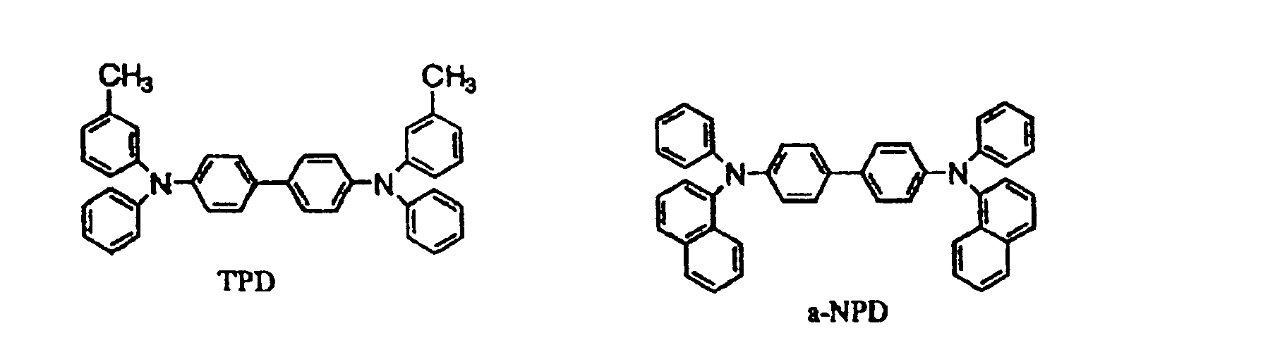
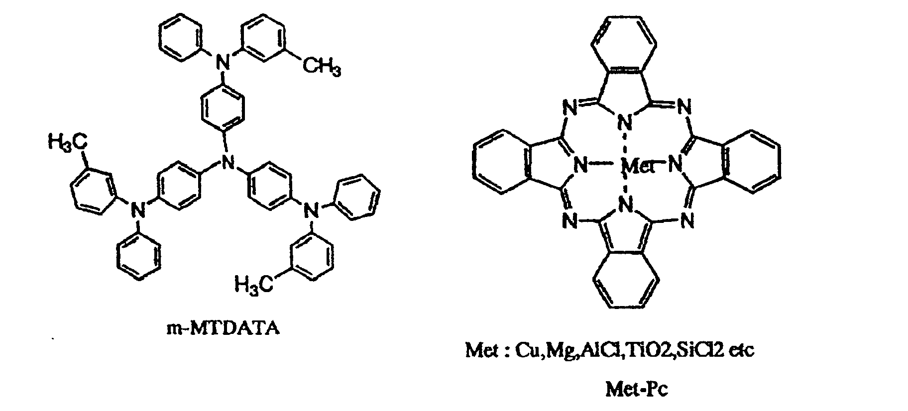
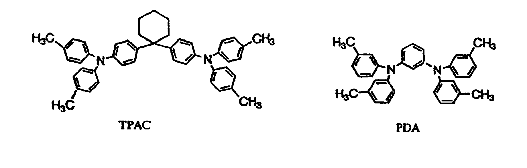
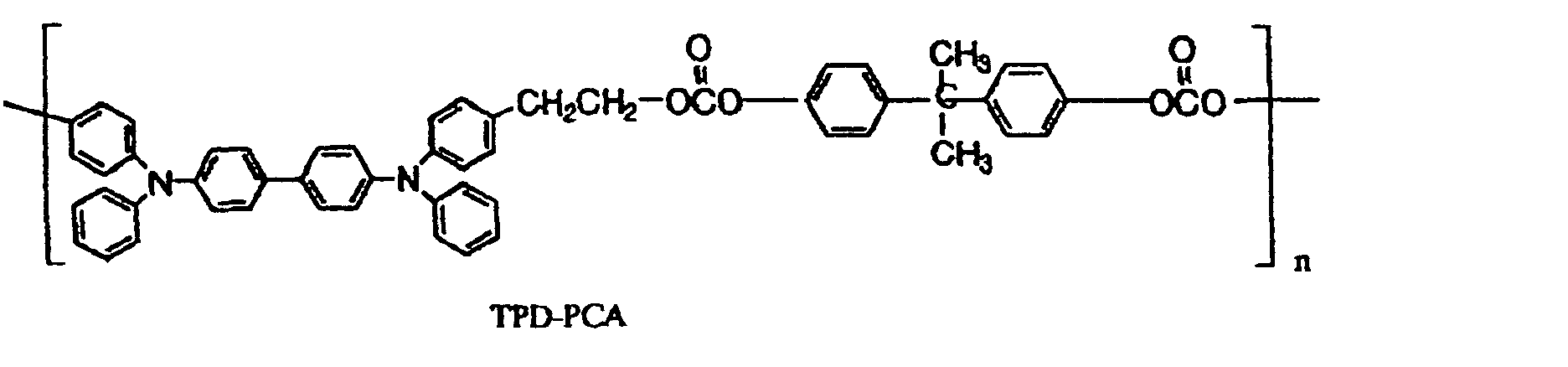
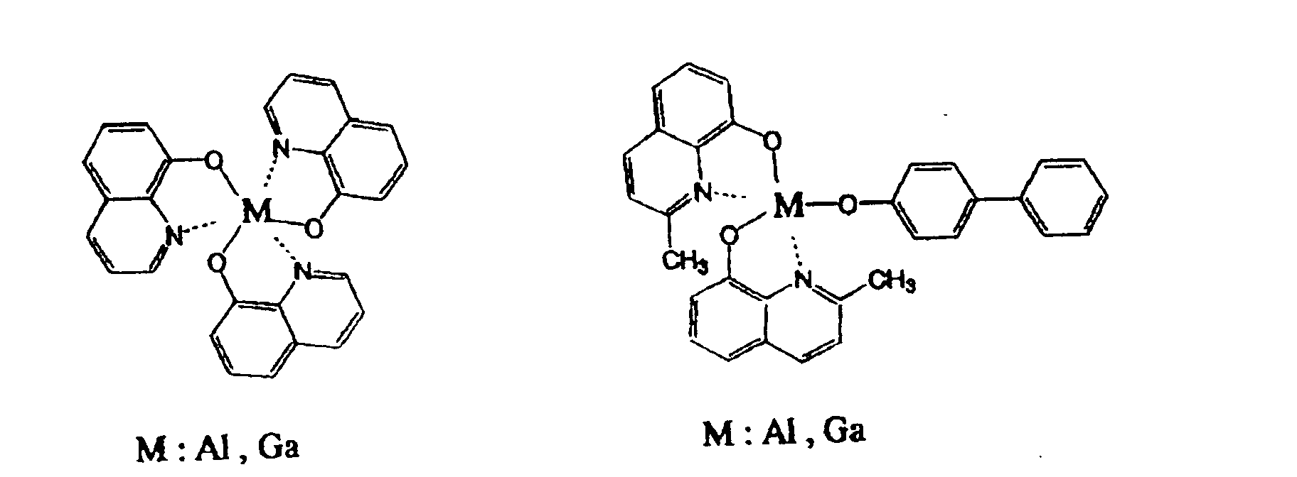
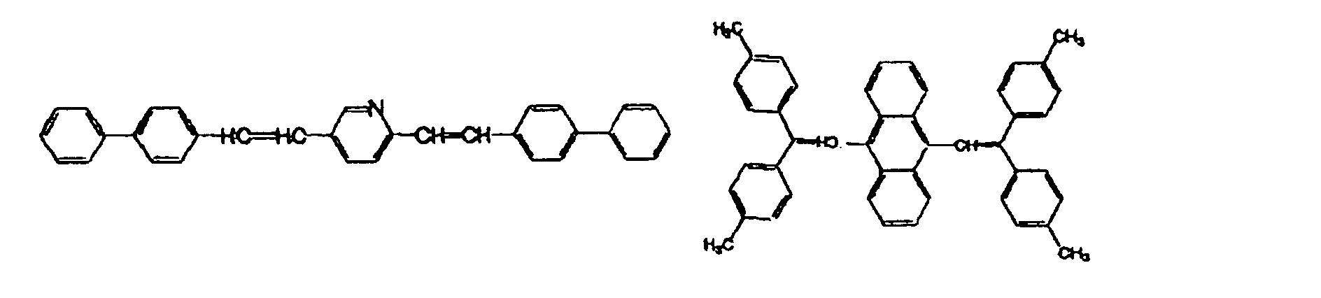
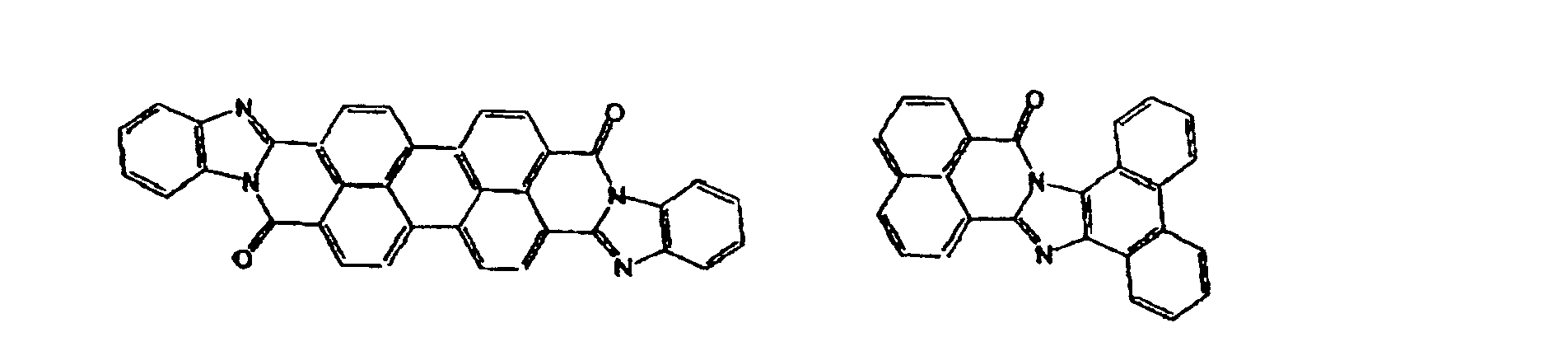
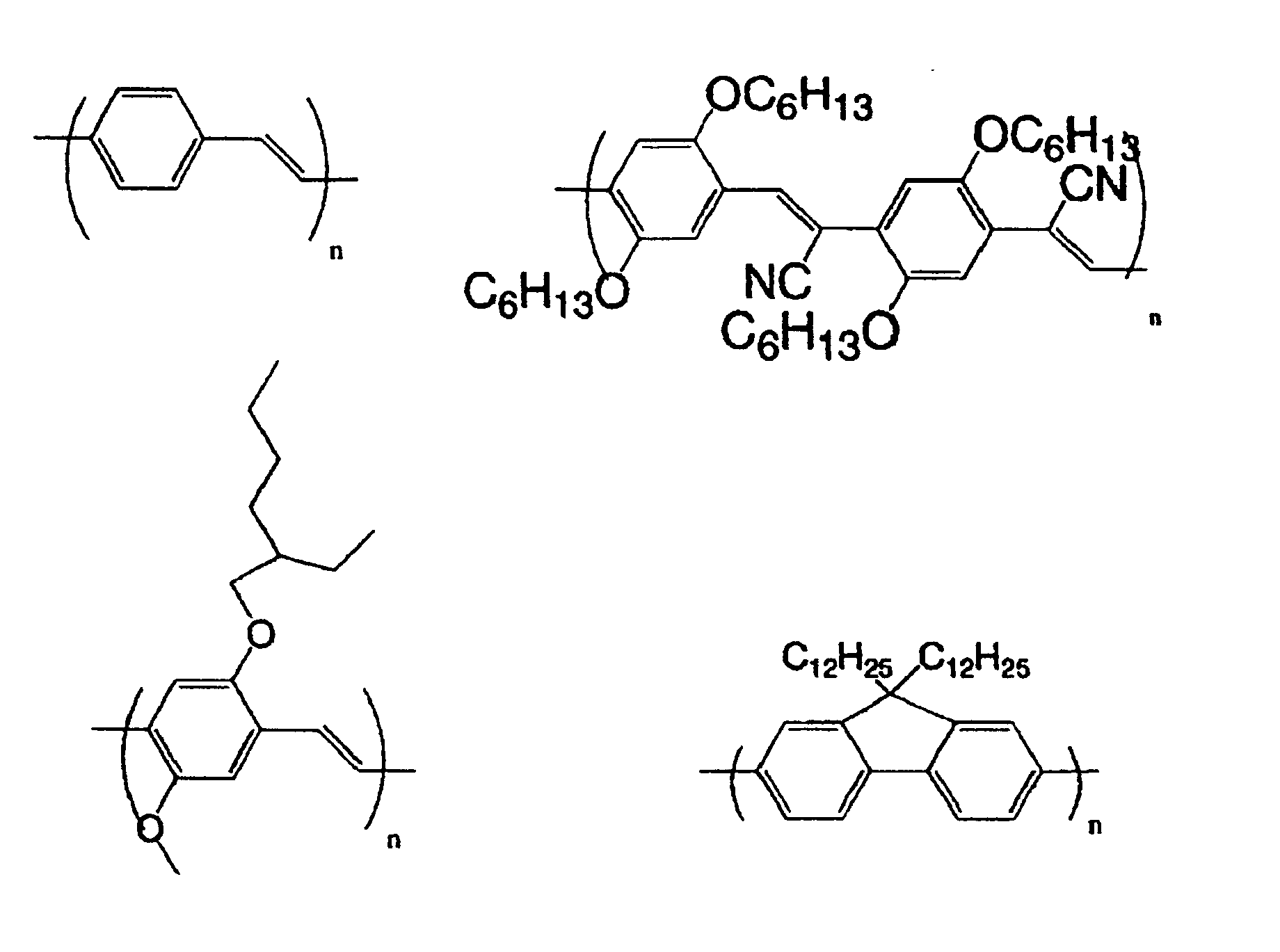
- the polymerized film of the organic compound having at least two polymerizable double bonds can also be used to constitute such a functional layer, as desired, in combination with a known hole-transporting compound, electron-transporting compound or luminescent compound, examples of which are enumerated hereinbelow.
- the polymerized film of organic compound having at least two polymerizable double bonds constitutes the first formed organic layer (i.e., the hole-transporting layer 5 in Figures 2 and 3), more preferably the first formed organic layer and the second formed organic layer (i.e., the hole-transporting layer 5 and the electron-transporting layer 6 in Figure 2; and the hole-transporting layer 5 and the luminescence layer 3 in Figure 3).
- the first formed organic layer comprises a polymerized film of organic compound having at least three polymerizable double bonds.
- the polymerized film of organic compound having at least two polymerizable double bonds constitutes at least three organic layers.
- an organic layer other than the organic layer(s) comprising the polymerized film of organic compound having at least two polymerizable double bonds may generally be formed into film by vacuum deposition or coating of a solution of the relevant compound in an appropriate solvent.
- the functional organic compound can be used in mixture with an appropriate binder resin to form a film.
- the organic compound may for example be used in 0.01 - 20 wt. parts, preferably, 0.1 - 10 wt. parts, per 1 wt. part of the binder resin.
- the binder resin used for the above purpose may be selected from a wide variety of scope. Examples thereof may include: polyvinyl carbazole resin, polycarbonate resin, polyester resin, polyarylate resin, polystyrene resin, acrylic resin, methacrylic resin, butyral resin, polyvinyl acetal resin, diallyl phthalate resin, phenolic resin, epoxy resin, silicone resin, polysulfone resin, and urea resin. These resins may be used singly or in combination of two or more species or in the form of copolymers.
- the anode As a material for the anode (2 shown in Figures 1 - 3), it is preferred to use one having as large a work function as possible, examples of which may include: metals, such as gold, platinum, nickel, palladium, cobalt, selenium and vanadium, and their alloys; metal oxides, such as tin oxide, zinc oxide, indium tin oxide (ITO), and indium zinc oxide; and electroconductive polymers, such as polyaniline, polypyrrole, polythiophene, and polyphenylene sulfide. These compounds may be used singly or in combination of two or more species.
- metals such as gold, platinum, nickel, palladium, cobalt, selenium and vanadium, and their alloys
- metal oxides such as tin oxide, zinc oxide, indium tin oxide (ITO), and indium zinc oxide
- electroconductive polymers such as polyaniline, polypyrrole, polythiophene, and polyphenylene sulfide.
- the cathode 4 shown in Figures 1 - 3 it is preferred to use one having a small work function, examples of which may include: metals, such as lithium, sodium, potassium, calcium, magnesium, aluminum, indium, silver, lead, tin and chromium, and their alloys. It is also possible to use metal oxide, such as indium tin oxide (ITO).
- ITO indium tin oxide
- the cathode may be formed in a single layer or a lamination of plural layers.
- the substrate 1 shown in Figures 1 - 3 for the organic luminescence device of the present invention may include an opaque substrate of metal, ceramics, etc., and a transparent substrate of glass, quartz, plastics, etc. It is possible to form the substrate with a color filter film, a fluorescent color conversion film, a dielectric reflection film, etc., thus controlling emitted luminescent light.
- the organic luminescence device of the present invention may further include a protective layer or a sealing layer.
- the protective layer may include: an inorganic film of diamond, metal oxide, metal nitride, etc.; a polymer film of fluorine-containing resin, polyparaxylene, polyethylene, silicone resin, polystyrene, etc., and a film of light-curable resin. It is also possible to effect packaging of the organic luminescence device per se with a sealing resin while covering the organic luminescence device with glass, gas-impermeable film, metal, etc.
- the organic layer in the luminescence device of the present invention can be effectively formed through two steps of film formation and curing by polymerization, and the resultant organic layer is little liable to cause agglomeration or crystallization resulting in defects, so that the luminescence device of the present invention can exhibit a much higher durability than the conventional device.
- the product solid was purified by silica gel column chromatography with ethyl-acetate and toluene as developing solvents, followed by condensation and crystallization by addition of hexane. The crystal was filtered out and dried to obtain 3.5 g (yield: 65.8 %) of yellow crystal of N,N'-diphenyl-N,N'-bis(4-formylphenyl)-4,4'-diamino-1,1-biphenyl.
- reaction liquid was poured into water and extracted with toluene.
- the resultant organic phase was washed three times with water and then purified by silica gel column chromatography with toluene and hexane as developing solvents, followed by condensation and crystallization by addition of hexane, to obtain 2.33 g (yield: 67.0 %) of N,N'-diphenyl-N,N'-bis(4-vinylphenyl)-4,4'-diamino-1,1-biphenyl.
- An organic luminescence device of a structure as shown in Figure 2 was prepared in the following manner.
- a 1.1 mm-thick glass substrate coated with a 120 nm-thick film of ITO (indium tin oxide) formed by sputtering was successively washed with acetone and isopropyl alcohol (IPA) under application of ultrasonic wave and then washed with IPA under boiling, followed by drying and cleaning by UV/ozone (i.e., irradiation with ultraviolet rays in the ozone-containing atmosphere), to obtain a transparent conductive substrate (including a substrate 1 and an ITO anode 2 formed thereon).
- ITO indium tin oxide
- N,N'-diphenyl-N,N'-bis(4-vinylphenyl)-4,4'-diamino-l,l'-biphenyl (DPDVDAB) as an organic layer having two polymerizable double bonds was dissolved at a concentration of 1.0 wt. % in toluene to form a coating liquid.
- the coating liquid was applied by spin coating (at 2000 rpm) on the above-treated ITO-coated transparent conductive substrate, followed by drying at 80 °C for 10 min. to form a film which was then heat-treated at 120 °C for 10 hours in a nitrogen atmosphere to form a 50 nm-thick polymerized film as a hole-transporting layer (layer 5).
- the vacuum deposition was respectively performed at a vacuum of 1.0x10 -4 Pa.
- An ITO-coated transparent conductive substrate identical to the one used in Example 1 was coated with DPDVDAB used in Example 1 by vacuum deposition at a film growth rate of 0.3 nm/sec in a vacuum of 1.0x10 -4 Pa to form a film thereof, which was then irradiated with ultraviolet rays for 5 min. and then heat-treated at 120 °C for 2 hours to form a 50 nm-thick polymerized film (as a hole-transporting layer 5).
- the polymerized film was coated by vacuum deposition successively with a 50 nm-thick film of Alq 3 (electron-transporting luminescent layer 6) and a 150 nm-thick Al-Li alloy (cathode film 4) similarly as in Example 1 to form an organic luminescence device having a structure as shown in Figure 2.
- An organic luminescence device having a structure as shown in Figure 2 was prepared in a similar manner as in Example 1 except for using N,N'-diphenyl-N,N'-bis(3-methylphenyl)-4,4'-diamino-1,1'-biphenyl instead of DPDVDAB and omitting the polymerization heating treatment for forming a hole-transporting layer 5.
- Example Applied voltage (V) Luminance (cd/m 2 ) Initial After 100 hours 1 5.0 755 730 2 5.0 740 710 Comp. 1 5.0 130 25
- the device was driven by applying a DC voltage of 10 volts between the ITO electrode 2 and the Al-Li cathode 4, whereby a current of 160 mA/cm 2 was flowed to exhibit orange luminescence at a luminance of 2700 cd/m 2 .
- N,N,N',N'-tetrakis[3-methacryloyloxyphenyl]-4,4'-diamino-1,1'-biphenyl (TMDAB) and benzoyl peroxide (in 2 wt. % of TMDAB) were dissolved in toluene to form a 1.0 wt. %-coating liquid.
- the coating liquid was applied by spin coating (2000 rpm) on an ITO-coated transparent conductive substrate identical to the one used in Example 1, followed by drying at 80 °C for 10 min. and heat-treatment at 120 °C for 8 hours, respectively in a nitrogen atmosphere, to form a 65 nm-thick polymerized film (hole-transporting layer 5).
- the polymerized film was coated with a 200 nm-thick cathode film of Mg/Ag alloy (9/1 by weight) by co-vacuum deposition at a film growth rate of 1.0 - 1.2 nm/sec in a vacuum of 1.0x10 -4 Pa to form an organic luminescence device having a structure as shown in Figure 2.
- the device was driven by applying a DC voltage of 10 volts between the ITO electrode 2 and the Mg/Ag-cathode, whereby a current of 230 mA/cm 2 was flowed to exhibit blue luminescence at a luminance of 3590 cd/m 2 .
- Example 4 The process of Example 4 was repeated up to the formation of the 65 nm-thick hole-transporting layer.
- BSOXD 2,5-bis(4-styrylphenyl)-1,3,4-oxadiazole
- coumarin 6 in 1 wt. % of BSOXD
- the coating liquid was applied by spin coating (2000 rpm) on the above-formed hole-transporting layer, followed by drying at 80 °C for 3 hours and heat-treatment at 120 °C for 8 hours respectively in a nitrogen atmosphere, to form a 50 nm-thick polymerized film (electron-transporting luminescent layer 6).
- the polymerized film was coated with a 200 nm-thick cathode film of Mg/Ag alloy (9/1 by weight) by co-vacuum deposition at a film growth rate of 1.0 - 1.2 nm/sec in a vacuum of 1.0x10 -4 Pa to form an organic luminescence device having a structure as shown in Figure 2.
- the device was driven by applying a DC voltage of 10 volts between the ITO electrode 2 and the Mg/Ag-cathode, whereby a current of 280 mA/cm 2 was flowed to exhibit green luminescence at a luminance of 39000 cd/m 2 .
- Example 4 The process of Example 4 was repeated up to the formation of the 65 nm-thick hole-transporting layer.
- BSOXD 2,5-bis(4-styrylphenyl)-1,3,4-oxadiazole
- 5,11-diphenyl-6,12-bis(4-vinylphenyl)naphthacene in 1 wt. % of BSOXD
- the coating liquid was applied by spin coating (2000 rpm) on the above-formed hole-transporting layer, followed by drying at 80 °C for 3 hours and heat-treatment at 120 °C for 8 hours respectively in a nitrogen atmosphere, to form a 50 nm-thick polymerized film (electron-transporting luminescent layer 6).
- the polymerized film was coated with a 200 nm-thick cathode film of Mg/Ag alloy (9/1 by weight) by co-vacuum deposition at a film growth rate of 1.0 - 1.2 nm/sec in a vacuum of 1.0x10 -4 Pa to form an organic luminescence device having a structure as shown in Figure 2.
- the device was driven by applying a DC voltage of 10 volts between the ITO electrode 2 and the Mg/Ag-cathode, whereby a current of 310 mA/cm 2 was flowed to exhibit yellow luminescence at a luminance of 42500 cd/m 2 .
- N,N,N',N'-tetrakis[3-vinylphenyl]-4,4'-diamino-1,1'-biphenyl (TBDAB) and benzoyl peroxide (in 2 wt. % of TBDAB) were dissolved in toluene to form a 1.0 wt. %-coating liquid.
- the coating liquid was applied by spin coating (2000 rpm) on an ITO-coated transparent conductive substrate identical to the one used in Example 1, followed by drying at 80 °C for 10 min. and heat-treatment at 120 °C for 8 hours, respectively in a nitrogen atmosphere, to form a 55 nm-thick polymerized film (hole-transporting layer 5).
- DPDMVB 4,4'-bis[2-phenyl-2-(4-methacryloyloxyphenyl)]vinyl-1,1'-biphenyl
- DPDMVB 5,11-diphenyl-6,12-bis(4-vinylphenyl)naphthacene
- the coating liquid was applied by spin coating (2000 rpm) on the above-formed hole-transporting layer, followed by drying at 80 °C for 3 hours and heat-treatment at 120 °C for 8 hours to form a 15 nm-thick polymerized film (luminescent layer 3).
- 1,3,5-tris(4-vinylphenyl-1,3,4-oxadiazoyl)benzene was dissolved in toluene to form a 0.3 wt. %-coating liquid.
- the coating liquid was applied by spin coating (1500 rpm) on the above-formed luminescent layer, followed by drying at 80 °C for 3 hours and heat-treatment at 120 °C for 8 hours to form a 35 nm-thick polymerized film (electron-transporting layer 6).
- the polymerized film was coated with a 0.3 nm-thick lithium fluoride film and then with a 200 nm-thick Al cathode film by vacuum deposition at a film growth rate of 1.0 - 1.2 nm/sec in a vacuum of 1.0x10 -4 Pa to form an organic luminescence device having a structure as shown in Figure 3.
- the device was driven by applying a DC voltage of 13 volts between the ITO electrode 2 and the Al-cathode, whereby a current of 530 mA/cm 2 was flowed to exhibit red luminescence at a luminance of 26000 cd/m 2 . Further, the device was continuously driven at a constant current of 50 mA/cm 2 whereby an initial luminance of 2500 cd/m 2 was only changed to 2450 cd/m 2 after 500 hours, thus showing a very small luminance lowering.
- Example 7 The process of Example 7 was repeated up to the formation of the 55 nm-thick hole-transporting layer.
- DPDMVB used in Example 7 and Nile Red (in 1 wt. % of DPDMVB) were dissolved in toluene to form a 0.2 wt. %-coating liquid.
- the coating liquid was applied by spin coating (2000 rpm) on the above-formed hole-transporting layer, followed by drying at 80 °C for 3 hours and heat-treatment at 120 °C for 8 hours respectively in a nitrogen atmosphere, to form a 15 nm-thick polymerized film (luminescent layer 3).
- the polymerized film was coated with a 40 nm-thick layer of aluminum quinolinol (Alq 3 ) (electron-transporting layer 6).
- the electron-transporting layer 6 was coated with a 0.3 nm-thick lithium fluoride layer and a 200 nm-thick Al cathode film 4 similarly as in Example 7 to form an organic luminescence device having a structure as shown in Figure 3.
- the device was driven by applying a DC voltage of 13 volts between the ITO electrode 2 and the Al-cathode, whereby a current of 930 mA/cm 2 was flowed to exhibit yellow luminescence at a luminance of 139000 cd/m 2 . Further, the device was continuously driven at a constant current of 50 mA/cm 2 whereby an initial luminance of 3100 cd/m 2 was only changed to 2950 cd/m 2 after 500 hours, thus showing a very small luminance lowering.
- An organic luminescence device capable of luminescence at a high efficiency, a high luminance and high durability is formed by a pair of electrodes comprising an anode and a cathode, and at least one organic layer disposed between the electrodes.
- the at least one organic layer includes at least one layer comprising a polymerized film of organic layer having at least two polymerizable double bonds.
Landscapes
- Chemical & Material Sciences (AREA)
- Engineering & Computer Science (AREA)
- Materials Engineering (AREA)
- Organic Chemistry (AREA)
- Electroluminescent Light Sources (AREA)
Abstract
Description










| Example | Applied voltage (V) | Luminance (cd/m2) | |
| Initial | After 100 hours | ||
| 1 | 5.0 | 755 | 730 |
| 2 | 5.0 | 740 | 710 |
| Comp. 1 | 5.0 | 130 | 25 |
Claims (12)
- An organic luminescence device, comprising: a pair of electrodes comprising an anode and a cathode, and at least one organic layer disposed between the electrodes, wherein said at least one organic layer includes at least one layer comprising a polymerized film of organic compound having at least two polymerizable double bonds.
- A luminescence device according to Claim 1, wherein said polymerizable double bonds comprise a carbon-to-carbon double bond.
- A luminescence device according to Claim 2, wherein said carbon-to-carbon double bond is an optionally substituted vinyl group, or an optionally substituted (meth)acrylate ester group.
- A luminescence device according to Claim 1, wherein said organic compound having at least two polymerizable double bonds is a hole-transporting compound, an electron-transporting compound or a luminescent compound.
- A luminescence device according to Claim 1, wherein said organic compound having at least two polymerizable double bonds is a hole-transporting luminescent compound or an electron-transporting luminescent compound.
- A luminescence device according to Claim 1, wherein said organic compound having at least two polymerizable double bonds is a luminescent compound having also hole-transporting and electron-transporting functions.
- A luminescence device according to Claim 1, wherein said polymerized film has been obtained by curing a film of said organic compound having at least two polymerizable double bonds formed by solution coating thereon by irradiation with actitinic light, heat or electron ray.
- A luminescence device according to Claim 1, wherein said at least one organic layer comprises at least two successively formed organic layers, to which a first formed organic layer comprises said polymerized film of organic compound having at least two polymerizable double bonds.
- A luminescence device according to Claim 8, wherein said at least two successively formed organic layers include a first formed organic layer and a second formed organic layer both comprising said polymerized film of organic compound having at least two polymerizable double bonds.
- A luminescence device according to Claim 8 or 9, wherein said first formed organic layer comprises a polymerized film of organic compound having at least three polymerizable double bonds.
- A luminescence device according to Claim 1, wherein said at least one organic layer comprises at least three organic layers each comprising said polymerized film of organic compound having at least two polymerizable double bonds.
- A process for producing an organic luminescence device of the type comprising a pair of electrodes comprising an anode and a cathode, and at least one organic layer disposed between the electrodes, said process comprising:a step of forming a film of organic compound having at least two polymerizable double bonds by application of a solution of the organic compound having at least two polymerizable double bonds, anda step of curing the film by irradiating the film with actinic light, heat or electron ray to polymerize the organic compound, thereby providing at least one of said at least one organic layer.
Applications Claiming Priority (2)
| Application Number | Priority Date | Filing Date | Title |
|---|---|---|---|
| JP2000112866 | 2000-04-14 | ||
| JP2000112866A JP4040235B2 (en) | 2000-04-14 | 2000-04-14 | Organic light emitting device |
Publications (3)
| Publication Number | Publication Date |
|---|---|
| EP1146574A2 true EP1146574A2 (en) | 2001-10-17 |
| EP1146574A3 EP1146574A3 (en) | 2003-02-19 |
| EP1146574B1 EP1146574B1 (en) | 2007-08-08 |
Family
ID=18624940
Family Applications (1)
| Application Number | Title | Priority Date | Filing Date |
|---|---|---|---|
| EP01109143A Expired - Lifetime EP1146574B1 (en) | 2000-04-14 | 2001-04-12 | Process for production of an organic luminescence device |
Country Status (6)
| Country | Link |
|---|---|
| US (2) | US20020045062A1 (en) |
| EP (1) | EP1146574B1 (en) |
| JP (1) | JP4040235B2 (en) |
| KR (1) | KR100416714B1 (en) |
| DE (1) | DE60129763T2 (en) |
| TW (1) | TW504943B (en) |
Cited By (6)
| Publication number | Priority date | Publication date | Assignee | Title |
|---|---|---|---|---|
| US6699597B2 (en) | 2001-08-16 | 2004-03-02 | 3M Innovative Properties Company | Method and materials for patterning of an amorphous, non-polymeric, organic matrix with electrically active material disposed therein |
| WO2004033583A3 (en) * | 2002-10-10 | 2004-07-08 | Enea Ente Nuove Tec | Method of preparing organic luminescent materials stabilized by heat treatment and materials obtained therefrom |
| US6855384B1 (en) * | 2000-09-15 | 2005-02-15 | 3M Innovative Properties Company | Selective thermal transfer of light emitting polymer blends |
| US7241512B2 (en) | 2002-04-19 | 2007-07-10 | 3M Innovative Properties Company | Electroluminescent materials and methods of manufacture and use |
| US7829203B2 (en) | 2002-03-09 | 2010-11-09 | Cdt Oxford Limited | Polymerisable compositions and organic light-emitting devices containing them |
| WO2013036043A2 (en) | 2011-09-09 | 2013-03-14 | 주식회사 엘지화학 | Material for organic light-emitting device, and organic light-emitting device using same |
Families Citing this family (20)
| Publication number | Priority date | Publication date | Assignee | Title |
|---|---|---|---|---|
| JP4678983B2 (en) * | 2001-05-14 | 2011-04-27 | 三井化学株式会社 | Organic electroluminescence device |
| JP5342420B2 (en) * | 2001-06-21 | 2013-11-13 | 昭和電工株式会社 | Organic light emitting device and light emitting material |
| JP2004103401A (en) * | 2002-09-10 | 2004-04-02 | Konica Minolta Holdings Inc | Device and method for manufacturing the device |
| US7014925B2 (en) | 2003-04-29 | 2006-03-21 | Canon Kabushiki Kaisha | Heterogeneous spiro compounds in organic light emitting device elements |
| CN100513514C (en) * | 2003-04-30 | 2009-07-15 | 昭和电工株式会社 | Organic polymer light-emitting element material having gold complex structure and organic polymer light-emitting element |
| EP1506991A3 (en) * | 2003-07-17 | 2005-08-10 | Fuji Photo Film Co., Ltd. | Liquid crystalline compound, liquid crystalline composition and retardation film |
| GB0418019D0 (en) * | 2004-08-12 | 2004-09-15 | Cdt Oxford Ltd | Method of making an optical device |
| US7285501B2 (en) * | 2004-09-17 | 2007-10-23 | Hewlett-Packard Development Company, L.P. | Method of forming a solution processed device |
| JP2007257897A (en) * | 2006-03-20 | 2007-10-04 | Seiko Epson Corp | LIGHT EMITTING DEVICE MANUFACTURING METHOD, LIGHT EMITTING DEVICE MANUFACTURING METHOD, AND ELECTRONIC DEVICE MANUFACTURING METHOD |
| WO2007119473A1 (en) | 2006-03-30 | 2007-10-25 | Konica Minolta Holdings, Inc. | Organic electroluminescence element, method for manufacturing organic electroluminescence element, illuminating device and display device |
| JP5332614B2 (en) | 2006-09-08 | 2013-11-06 | コニカミノルタ株式会社 | Organic electroluminescence element, lighting device and display device |
| WO2008090912A1 (en) * | 2007-01-23 | 2008-07-31 | Konica Minolta Holdings, Inc. | Method for manufacturing organic electroluminescent device, organic electroluminescent device manufactured by the method, display device and illuminating device |
| TWI474759B (en) * | 2007-02-15 | 2015-02-21 | 三菱化學股份有限公司 | Method for producing organic electroluminescence device and organic electroluminescence device |
| JP4946923B2 (en) * | 2007-03-07 | 2012-06-06 | 三菱化学株式会社 | Organic electroluminescence device |
| JP5151201B2 (en) * | 2007-03-26 | 2013-02-27 | セイコーエプソン株式会社 | Method for manufacturing organic electroluminescence element |
| US8242488B2 (en) | 2007-05-30 | 2012-08-14 | Konica Minolta Holdings, Inc. | Organic electroluminescent element, display device, and illuminating device |
| JP5402642B2 (en) * | 2007-11-12 | 2014-01-29 | コニカミノルタ株式会社 | Method for manufacturing organic electronics element |
| JP5287455B2 (en) * | 2008-04-16 | 2013-09-11 | 三菱化学株式会社 | Hole injection transport layer forming composition, method for manufacturing hole injection transport layer forming composition, organic electroluminescence device, organic EL display, and organic EL lighting |
| KR102074031B1 (en) | 2013-09-17 | 2020-02-05 | 가부시키가이샤 큐럭스 | Organic electroluminescence element |
| CN116096198A (en) * | 2021-11-03 | 2023-05-09 | Tcl科技集团股份有限公司 | Preparation method of electroluminescent device, electroluminescent device and display device |
Family Cites Families (11)
| Publication number | Priority date | Publication date | Assignee | Title |
|---|---|---|---|---|
| US4075013A (en) * | 1976-09-13 | 1978-02-21 | Ward Anthony T | Electrophotochemical preparation of selenium photoconductive members |
| JPS6017446A (en) * | 1983-07-11 | 1985-01-29 | Fuji Photo Film Co Ltd | Manufacture of support for photographic printing paper |
| EP0534316A1 (en) * | 1991-09-21 | 1993-03-31 | Hoechst Aktiengesellschaft | Use of alkylated polyethylenimines to concentrate bile acids |
| JPH0696860A (en) * | 1992-09-11 | 1994-04-08 | Toshiba Corp | Organic el element |
| DE4305959A1 (en) * | 1993-02-26 | 1994-09-01 | Bayer Ag | Luminescent copolymers |
| US5503910A (en) * | 1994-03-29 | 1996-04-02 | Idemitsu Kosan Co., Ltd. | Organic electroluminescence device |
| DE69535080T2 (en) * | 1994-12-28 | 2006-12-28 | Cambridge Display Technology Ltd. | Polymers for optical devices |
| DE19643097A1 (en) * | 1996-10-18 | 1998-04-23 | Basf Ag | Novel thermally-crosslinkable tri:aryl:amine(s) |
| US6403237B1 (en) * | 1998-06-10 | 2002-06-11 | Sumitomo Chemical Co., Ltd. | Polymeric fluorescent substance and organic electroluminescence device |
| US6107452A (en) * | 1998-10-09 | 2000-08-22 | International Business Machines Corporation | Thermally and/or photochemically crosslinked electroactive polymers in the manufacture of opto-electronic devices |
| US6399224B1 (en) * | 2000-02-29 | 2002-06-04 | Canon Kabushiki Kaisha | Conjugated polymers with tunable charge injection ability |
-
2000
- 2000-04-14 JP JP2000112866A patent/JP4040235B2/en not_active Expired - Fee Related
-
2001
- 2001-04-11 US US09/829,918 patent/US20020045062A1/en not_active Abandoned
- 2001-04-12 EP EP01109143A patent/EP1146574B1/en not_active Expired - Lifetime
- 2001-04-12 DE DE60129763T patent/DE60129763T2/en not_active Expired - Lifetime
- 2001-04-13 TW TW090108968A patent/TW504943B/en not_active IP Right Cessation
- 2001-04-14 KR KR10-2001-0020006A patent/KR100416714B1/en not_active Expired - Fee Related
-
2002
- 2002-09-23 US US10/252,046 patent/US20030044518A1/en not_active Abandoned
Cited By (17)
| Publication number | Priority date | Publication date | Assignee | Title |
|---|---|---|---|---|
| US6855384B1 (en) * | 2000-09-15 | 2005-02-15 | 3M Innovative Properties Company | Selective thermal transfer of light emitting polymer blends |
| US7445825B2 (en) | 2001-08-16 | 2008-11-04 | 3M Innovative Properties Company | Donor sheet having a polymerizable, amorphous matrix with electrically active material disposed therein |
| US7014978B2 (en) | 2001-08-16 | 2006-03-21 | 3M Innovative Properties Company | Method and materials for patterning of an amorphous, non-polymeric, organic matrix with electrically active material disposed therein |
| US6699597B2 (en) | 2001-08-16 | 2004-03-02 | 3M Innovative Properties Company | Method and materials for patterning of an amorphous, non-polymeric, organic matrix with electrically active material disposed therein |
| US7276322B2 (en) | 2001-08-16 | 2007-10-02 | 3M Innovative Properties Company | Method and materials for patterning of an amorphous, non-polymeric, organic matrix with electrically active material disposed therein |
| US6844128B2 (en) | 2001-08-16 | 2005-01-18 | 3M Innovative Properties Company | Method and materials for patterning of an amorphous, non-polymeric, organic matrix with electrically active material disposed therein |
| US7977864B2 (en) | 2001-08-16 | 2011-07-12 | Samsung Mobile Display Co., Ltd. | Method and materials for patterning of an amorphous, non-polymeric, organic matrix with electrically active material disposed therein |
| US7829203B2 (en) | 2002-03-09 | 2010-11-09 | Cdt Oxford Limited | Polymerisable compositions and organic light-emitting devices containing them |
| US8883321B2 (en) | 2002-03-09 | 2014-11-11 | Cdt Oxford Limited | Polymerizable compositions and organic light-emitting devices containing them |
| US7241512B2 (en) | 2002-04-19 | 2007-07-10 | 3M Innovative Properties Company | Electroluminescent materials and methods of manufacture and use |
| US7442421B2 (en) | 2002-04-19 | 2008-10-28 | 3M Innovative Properties Company | Electroluminescent materials and methods of manufacture and use |
| WO2004033583A3 (en) * | 2002-10-10 | 2004-07-08 | Enea Ente Nuove Tec | Method of preparing organic luminescent materials stabilized by heat treatment and materials obtained therefrom |
| WO2013036043A2 (en) | 2011-09-09 | 2013-03-14 | 주식회사 엘지화학 | Material for organic light-emitting device, and organic light-emitting device using same |
| WO2013036044A2 (en) | 2011-09-09 | 2013-03-14 | 주식회사 엘지화학 | Material for organic light-emitting device, and organic light-emitting device using same |
| WO2013036045A2 (en) | 2011-09-09 | 2013-03-14 | 주식회사 엘지화학 | Material for organic light-emitting device, and organic light-emitting device using same |
| US9553270B2 (en) | 2011-09-09 | 2017-01-24 | Lg Chem, Ltd. | Material for organic light-emitting device, and organic light-emitting device using same |
| US9716232B2 (en) | 2011-09-09 | 2017-07-25 | Lg Chem, Ltd. | Material for organic light-emitting device, and organic light-emitting device using same |
Also Published As
| Publication number | Publication date |
|---|---|
| US20030044518A1 (en) | 2003-03-06 |
| US20020045062A1 (en) | 2002-04-18 |
| KR20010098607A (en) | 2001-11-08 |
| JP4040235B2 (en) | 2008-01-30 |
| EP1146574A3 (en) | 2003-02-19 |
| DE60129763D1 (en) | 2007-09-20 |
| KR100416714B1 (en) | 2004-01-31 |
| JP2001297882A (en) | 2001-10-26 |
| TW504943B (en) | 2002-10-01 |
| EP1146574B1 (en) | 2007-08-08 |
| DE60129763T2 (en) | 2008-04-30 |
Similar Documents
| Publication | Publication Date | Title |
|---|---|---|
| EP1146574B1 (en) | Process for production of an organic luminescence device | |
| US6800379B2 (en) | Compound having pyrrole ring and light-emitting device comprising same | |
| US6652997B2 (en) | Organic luminescence device | |
| Noda et al. | A Blue‐Emitting Organic Electroluminescent Device Using a Novel Emitting Amorphous Molecular Material, 5, 5'‐Bis (dimesitylboryl)‐2, 2'‐bithiophene | |
| US20020177009A1 (en) | Fused polynuclear compound and organic luminescence device | |
| JP2000068065A (en) | Organic EL device | |
| JP2002255934A (en) | New compound, its polymer, light emission element material using these substances and the light emission element | |
| JP2003138251A (en) | Organic light emitting device | |
| JP2000286056A (en) | Electroluminescent element material and electroluminescent element | |
| JP2002293888A (en) | Novel polymer, light emitting device material and light emitting device using the same | |
| JPH07147189A (en) | Organic electroluminescent device | |
| JP4144987B2 (en) | Organic light emitting device materials and organic light emitting devices using them | |
| JP2002208481A (en) | Organic light emitting device and method of manufacturing the same | |
| JP2004103401A (en) | Device and method for manufacturing the device | |
| JP2001284052A (en) | Organic light emitting device | |
| JP2002212150A (en) | Triarylamine compound, polymer film using the triarylamine compound, organic light emitting device, and method of manufacturing the same | |
| WO2003029383A1 (en) | Organic luminescence device | |
| JP2001278889A (en) | New silicon compound, organic luminescent element material and organic luminescent element using the same | |
| CN100334065C (en) | Dibenzoperylene compound, organic electroluminescent device and organic electroluminescent display | |
| JP3646339B2 (en) | Organic thin film EL device | |
| EP1138683B1 (en) | Organic luminescence device using novel organic boron compounds and process for producing these compounds | |
| JP2003123972A (en) | Organic light emitting device | |
| JP2001172285A (en) | Organic light emission element material and organic light emission element using the same | |
| JPH07282977A (en) | Organic electroluminescence device material and organic electroluminescence device using the same | |
| Peng | Organic/Polymer Luminescent Materials and Devices |
Legal Events
| Date | Code | Title | Description |
|---|---|---|---|
| PUAI | Public reference made under article 153(3) epc to a published international application that has entered the european phase |
Free format text: ORIGINAL CODE: 0009012 |
|
| 17P | Request for examination filed |
Effective date: 20010412 |
|
| AK | Designated contracting states |
Kind code of ref document: A2 Designated state(s): AT BE CH CY DE DK ES FI FR GB GR IE IT LI LU MC NL PT SE TR |
|
| AX | Request for extension of the european patent |
Free format text: AL;LT;LV;MK;RO;SI |
|
| PUAL | Search report despatched |
Free format text: ORIGINAL CODE: 0009013 |
|
| RIC1 | Information provided on ipc code assigned before grant |
Ipc: 7C 09K 11/06 B Ipc: 7H 05B 33/14 B Ipc: 7H 01L 51/20 A |
|
| AK | Designated contracting states |
Designated state(s): AT BE CH CY DE DK ES FI FR GB GR IE IT LI LU MC NL PT SE TR |
|
| AX | Request for extension of the european patent |
Extension state: AL LT LV MK RO SI |
|
| 17Q | First examination report despatched |
Effective date: 20030512 |
|
| AKX | Designation fees paid |
Designated state(s): DE FI FR GB IT |
|
| GRAP | Despatch of communication of intention to grant a patent |
Free format text: ORIGINAL CODE: EPIDOSNIGR1 |
|
| RTI1 | Title (correction) |
Free format text: PROCESS FOR PRODUCTION OF AN ORGANIC LUMINESCENCE DEVICE |
|
| RIC1 | Information provided on ipc code assigned before grant |
Ipc: H05B 33/14 20060101ALI20070115BHEP Ipc: C09K 11/06 20060101ALI20070115BHEP Ipc: H01L 51/00 20060101AFI20070115BHEP |
|
| GRAS | Grant fee paid |
Free format text: ORIGINAL CODE: EPIDOSNIGR3 |
|
| GRAA | (expected) grant |
Free format text: ORIGINAL CODE: 0009210 |
|
| RIN1 | Information on inventor provided before grant (corrected) |
Inventor name: TANABE, HIROSHI Inventor name: SENOO, AKIHIRO Inventor name: KAWAI, TATSUNDO Inventor name: UENO, KAZUNORI Inventor name: OSATO, YOICHI Inventor name: MASHIMO, SEIJI Inventor name: SUZUKI, KOICHI Inventor name: HASHIMOTO, YUICHI |
|
| AK | Designated contracting states |
Kind code of ref document: B1 Designated state(s): DE FI FR GB IT |
|
| REG | Reference to a national code |
Ref country code: GB Ref legal event code: FG4D |
|
| REF | Corresponds to: |
Ref document number: 60129763 Country of ref document: DE Date of ref document: 20070920 Kind code of ref document: P |
|
| ET | Fr: translation filed | ||
| PG25 | Lapsed in a contracting state [announced via postgrant information from national office to epo] |
Ref country code: FI Free format text: LAPSE BECAUSE OF FAILURE TO SUBMIT A TRANSLATION OF THE DESCRIPTION OR TO PAY THE FEE WITHIN THE PRESCRIBED TIME-LIMIT Effective date: 20070808 |
|
| PLBE | No opposition filed within time limit |
Free format text: ORIGINAL CODE: 0009261 |
|
| STAA | Information on the status of an ep patent application or granted ep patent |
Free format text: STATUS: NO OPPOSITION FILED WITHIN TIME LIMIT |
|
| 26N | No opposition filed |
Effective date: 20080509 |
|
| PG25 | Lapsed in a contracting state [announced via postgrant information from national office to epo] |
Ref country code: IT Free format text: LAPSE BECAUSE OF NON-PAYMENT OF DUE FEES Effective date: 20080430 |
|
| PGFP | Annual fee paid to national office [announced via postgrant information from national office to epo] |
Ref country code: GB Payment date: 20140414 Year of fee payment: 14 |
|
| PGFP | Annual fee paid to national office [announced via postgrant information from national office to epo] |
Ref country code: FR Payment date: 20140428 Year of fee payment: 14 Ref country code: DE Payment date: 20140430 Year of fee payment: 14 |
|
| REG | Reference to a national code |
Ref country code: DE Ref legal event code: R119 Ref document number: 60129763 Country of ref document: DE |
|
| GBPC | Gb: european patent ceased through non-payment of renewal fee |
Effective date: 20150412 |
|
| PG25 | Lapsed in a contracting state [announced via postgrant information from national office to epo] |
Ref country code: GB Free format text: LAPSE BECAUSE OF NON-PAYMENT OF DUE FEES Effective date: 20150412 Ref country code: DE Free format text: LAPSE BECAUSE OF NON-PAYMENT OF DUE FEES Effective date: 20151103 |
|
| REG | Reference to a national code |
Ref country code: FR Ref legal event code: ST Effective date: 20151231 |
|
| PG25 | Lapsed in a contracting state [announced via postgrant information from national office to epo] |
Ref country code: FR Free format text: LAPSE BECAUSE OF NON-PAYMENT OF DUE FEES Effective date: 20150430 |