EP1139173A2 - Mikrolithographisches Beleuchtungssystem und damit versehene mikrolithographische Projektionsbelichtungsanlage - Google Patents
Mikrolithographisches Beleuchtungssystem und damit versehene mikrolithographische Projektionsbelichtungsanlage Download PDFInfo
- Publication number
- EP1139173A2 EP1139173A2 EP01103182A EP01103182A EP1139173A2 EP 1139173 A2 EP1139173 A2 EP 1139173A2 EP 01103182 A EP01103182 A EP 01103182A EP 01103182 A EP01103182 A EP 01103182A EP 1139173 A2 EP1139173 A2 EP 1139173A2
- Authority
- EP
- European Patent Office
- Prior art keywords
- microlithographic
- optical element
- lighting system
- ill
- asymmetrical
- Prior art date
- Legal status (The legal status is an assumption and is not a legal conclusion. Google has not performed a legal analysis and makes no representation as to the accuracy of the status listed.)
- Withdrawn
Links
Images

Classifications
-
- G—PHYSICS
- G03—PHOTOGRAPHY; CINEMATOGRAPHY; ANALOGOUS TECHNIQUES USING WAVES OTHER THAN OPTICAL WAVES; ELECTROGRAPHY; HOLOGRAPHY
- G03F—PHOTOMECHANICAL PRODUCTION OF TEXTURED OR PATTERNED SURFACES, e.g. FOR PRINTING, FOR PROCESSING OF SEMICONDUCTOR DEVICES; MATERIALS THEREFOR; ORIGINALS THEREFOR; APPARATUS SPECIALLY ADAPTED THEREFOR
- G03F7/00—Photomechanical, e.g. photolithographic, production of textured or patterned surfaces, e.g. printing surfaces; Materials therefor, e.g. comprising photoresists; Apparatus specially adapted therefor
- G03F7/20—Exposure; Apparatus therefor
-
- G—PHYSICS
- G03—PHOTOGRAPHY; CINEMATOGRAPHY; ANALOGOUS TECHNIQUES USING WAVES OTHER THAN OPTICAL WAVES; ELECTROGRAPHY; HOLOGRAPHY
- G03F—PHOTOMECHANICAL PRODUCTION OF TEXTURED OR PATTERNED SURFACES, e.g. FOR PRINTING, FOR PROCESSING OF SEMICONDUCTOR DEVICES; MATERIALS THEREFOR; ORIGINALS THEREFOR; APPARATUS SPECIALLY ADAPTED THEREFOR
- G03F7/00—Photomechanical, e.g. photolithographic, production of textured or patterned surfaces, e.g. printing surfaces; Materials therefor, e.g. comprising photoresists; Apparatus specially adapted therefor
- G03F7/70—Microphotolithographic exposure; Apparatus therefor
- G03F7/70058—Mask illumination systems
- G03F7/70066—Size and form of the illuminated area in the mask plane, e.g. reticle masking blades or blinds
-
- G—PHYSICS
- G02—OPTICS
- G02B—OPTICAL ELEMENTS, SYSTEMS OR APPARATUS
- G02B27/00—Optical systems or apparatus not provided for by any of the groups G02B1/00 - G02B26/00, G02B30/00
- G02B27/0025—Optical systems or apparatus not provided for by any of the groups G02B1/00 - G02B26/00, G02B30/00 for optical correction, e.g. distorsion, aberration
-
- G—PHYSICS
- G03—PHOTOGRAPHY; CINEMATOGRAPHY; ANALOGOUS TECHNIQUES USING WAVES OTHER THAN OPTICAL WAVES; ELECTROGRAPHY; HOLOGRAPHY
- G03F—PHOTOMECHANICAL PRODUCTION OF TEXTURED OR PATTERNED SURFACES, e.g. FOR PRINTING, FOR PROCESSING OF SEMICONDUCTOR DEVICES; MATERIALS THEREFOR; ORIGINALS THEREFOR; APPARATUS SPECIALLY ADAPTED THEREFOR
- G03F7/00—Photomechanical, e.g. photolithographic, production of textured or patterned surfaces, e.g. printing surfaces; Materials therefor, e.g. comprising photoresists; Apparatus specially adapted therefor
- G03F7/70—Microphotolithographic exposure; Apparatus therefor
- G03F7/70058—Mask illumination systems
- G03F7/70091—Illumination settings, i.e. intensity distribution in the pupil plane or angular distribution in the field plane; On-axis or off-axis settings, e.g. annular, dipole or quadrupole settings; Partial coherence control, i.e. sigma or numerical aperture [NA]
- G03F7/70108—Off-axis setting using a light-guiding element, e.g. diffractive optical elements [DOEs] or light guides
-
- G—PHYSICS
- G03—PHOTOGRAPHY; CINEMATOGRAPHY; ANALOGOUS TECHNIQUES USING WAVES OTHER THAN OPTICAL WAVES; ELECTROGRAPHY; HOLOGRAPHY
- G03F—PHOTOMECHANICAL PRODUCTION OF TEXTURED OR PATTERNED SURFACES, e.g. FOR PRINTING, FOR PROCESSING OF SEMICONDUCTOR DEVICES; MATERIALS THEREFOR; ORIGINALS THEREFOR; APPARATUS SPECIALLY ADAPTED THEREFOR
- G03F7/00—Photomechanical, e.g. photolithographic, production of textured or patterned surfaces, e.g. printing surfaces; Materials therefor, e.g. comprising photoresists; Apparatus specially adapted therefor
- G03F7/70—Microphotolithographic exposure; Apparatus therefor
- G03F7/70216—Mask projection systems
- G03F7/70225—Optical aspects of catadioptric systems, i.e. comprising reflective and refractive elements
Definitions
- the invention relates to a microlithographic lighting system with an optical Axis and symmetrically arranged optical elements and with a Image field level according to the preamble of claim 1.
- Such lighting systems and projection exposure systems are, for example, from DE 198 55 106 A of the applicant and the documents cited therein are known.
- EP 0 964 282 A2 also includes such a lighting system in one Projection exposure system known, the projection lens according to the characterizing features of claims 14 and 15 specified here.
- the lighting system and projection lens have a common optical axis (A in Fig. 1).
- Lenses with mirrors cannot be unvignetted at the same time around the optical axis have centered field and pupil planes (except when using a physical Beam splitter). Therefore, e.g. in EP 0 964 282 A the object and image field rectangle lying outside the optical axis.
- the lighting field generated by the axisymmetric lighting system includes how this off-axis rectangle is shown in FIG.
- This circular field is significantly larger than a minimal circular field, which the rectangle encompasses centrally.
- the size of the lenses and mirrors of an optical system increases with the field. In order to the image errors or the correction effort also grow.
- the aberrations of optical systems consisting of axisymmetric elements are axisymmetric. Are the optical axes of the lighting system and Projection lens against each other in favor of the small lighting system offset in parallel, the errors of the two are not of the same symmetry and can therefore not be compared. For microlithography projection exposure systems the telecentricity error is particularly critical here.
- the lighting system and the projection lens are now despite axis offset in the symmetry of their respective image error distribution in the Reticle level adapted to each other.
- an optical element in accordance with the lighting system Claim 1 is arranged close to the field and executed asymmetrically to the optical axis is.
- This element is from an off-axis grid element, as for example in Honeycomb condensers used in lighting systems are distinguished by the element according to the invention the whole light beam from a single steady differentiable cross-sectional area is detected.
- Such elements are special Lenses, prisms, plates and mirrors, all with aspherical surfaces both rotationally symmetrical type as well as free-form surfaces. Equivalents are equivalent Fresnel lenses, binary or step-shaped optical elements and diffractive elements, too in combination.
- Claim 2 specifies the location of the asymmetrically designed element in that it is adjacent to the image plane of the lighting system or to one of them equivalent field level is arranged.
- Preferred embodiments of the invention according to subclaims 7 to 10 see one decentered spherical or rotationally symmetrical aspherical, e.g. toric lens or a wedge plate (prism) in front, and a free-form correction surface (general asphere) in Connection with the forms mentioned or independently.
- the asymmetrical or decentered element is close to the field in one End of the lighting system forming REMA lens arranged, preferably as the first or last lens of this REMA lens.
- REMA lens arranged, preferably as the first or last lens of this REMA lens.
- the lighting system is telecentric with a defined deviation and thus adapted to a corresponding projection lens.
- catadioptric lenses are preferred Projection lenses in question, as specified in claim 14.
- Preferred Embodiments of the catadioptric lenses are such according to claim 15 with exactly one concave mirror and at least two folding mirrors - such as in the EP 0 964 282 A - or those without a folding mirror with a continuous one Axis of symmetry of all optical elements according to claim 16.
- Suitable lenses namely catoptric or catadioptric derived from them Lenses with a plurality of curved mirrors are e.g. also from EP 0 779 528 A or US 4,701,035 are known.
- Claim 19 specifies the object-side telecentricity of the projection lens to which it fits is the telecentricity of the lighting system according to claim 12 and for which the invention should preferably be used.
- a microlithographic structuring method according to the invention is the subject of Claim 20.
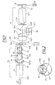
- the schematic lens section of FIG. 1 shows the invention using an example Projection exposure system.
- the light source LS is usually an excimer laser, e.g. with 193 nm or 157 nm Wavelength or another available light source at a UV wavelength.
- the lighting system ILL is centered on the optical axis OAI arranged.
- This optical axis OAI is usually angled with folding mirrors, to a complete machine with practical dimensions and high stability enable.
- a subsystem IS of the ILL lighting system is used for beam shaping, Increasing the light conductance, setting the type of lighting (conventional, ring aperture, Dipole, quadrupole) and degree of coherence and homogenization.
- a reticle masking system REMA is arranged in a field level if necessary, the field OF illuminated on the reticle Ret is adjustable.
- a uniformity filter UF can be arranged nearby and the uniformity of the Ensure lighting intensity in the reticle plane Ret. It can be used as an absorption gradient filter provided by vapor deposition of a metal layer on a flat plate become.
- the following REMA lens RO is used for the sharp image of the Reticle mask REMA limited field on the reticle level or the reticle Ret. It consists of a part RO 'of lenses centered on the optical axis OAI and one Adaptation element AE asymmetrical to the field to the optical axis OAI. The latter is here the reticle plane Ret is adjacent at a distance a. Between the aperture level IA and in any case at least one lens IAL is arranged in the adaptation element AE. The Element AE has an offset ⁇ A against the optical axis OAI. In the area of REMA lens is also shown schematically the light beam LB, which is the total asymmetrical adaptation element AE due to its continuously differentiable optical Interfaces. So the arrangement is not comparable to a lens array, as is customary in a honeycomb condenser, and in which a plurality of Lenses are also arranged next to one another along the optical axis.
- the reticle Ret which bears the mask of the structure to be imaged, held by a positioning and movement system ORet
- the projection objective P is arranged below, here a catadioptric system with Concave mirror M1, two folding mirrors FM1 and FM2 and with the lens groups LG1, LG2 and LG3.
- the optical axis OAP of the projection system P is between the Folding mirrors FM1, FM2 deflected to the minor axis OAP '.
- Object field OF, intermediate image Imi and image Im on the wafer W arranged in the image plane, which is from the Operating system OW positioned and moved are each opposite the optical one Axis OAP of the projection lens P laterally offset.
- This offset has the Object field OF has the value ⁇ y and is required so that in the area of the concave mirror M1 and the lens group LG2 reciprocating light beams from the folding mirrors FM1 and FM2 can be separated.
- the special features are the parallel offset of the optical axes OAI Illumination system Ill and OAP of the projection lens P at the reticle plane Ret and the adaptation element AE in the lighting system Ill.
- Fig. 2 is a section through the reticle plane Ret, the effect achieved thereby shows.
- the narrow rectangular object field OF of, for example, 35 x 110 mm 2 - adapted for a wafer scanner with a 1: 5 projection objective P - is offset by the value ⁇ y against the optical axis OAP of the projection objective P.
- This object field OF is inscribed in a circle around the optical axis OAP with the radius RP touching the edge. This circle represents the object field of the projection lens P which is relevant for the imaging geometry and the image errors, which, however, cannot be better used for the reasons mentioned above.
- the same circle with radius RP is conventionally the image field of the lighting system, compare EP 0 964 282 A2.
- At least the REMA lens must have the required size and have the corresponding correction effort.
- the illumination system Ill has the smaller image field with the Radius RI, which is exactly what is created by the REMA system REMA Rectangle OF, that is, the object field OF used by the projection lens P, comprises. His The center lies on the optical axis OAI of the illumination system Ill and is just around that Offset ⁇ y of the object field OF with respect to the optical axis OAP of the Projection lens P offset.
- FIGS RO A specific exemplary embodiment of a REMA objective is shown on the basis of FIGS RO described with adaptation element AE.
- a sophisticated projection lens P of microlithography is bilateral telecentric.
- small disturbances of the Pupil deformation of the aperture level
- an object-side deviation from the Telecentric approved. This manifests itself in an optical axis OAP rotationally symmetrical deviation of the Main beam angle of approx. 0.1 to 50 mrad from the parallel to the optical axis OAP.
- This pupil function or deviation from telecentricity can be from Illumination system Ill, especially from the REMA RO lens. This is described for example in DE 196 53 983 A.
- Table 1 gives the design data of this REMA lens RO.
- IAL a lens element centered on the optical axis OAI is between the Image field Fourier-transformed aperture plane IA and the adaptation element AE referred to, which is specified in the characterizing part of claim 5.
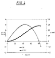
- FIG. 4 shows a typical pupil function PF of a projection objective P, for which the REMA lens shown above is adapted.
- the course is but not homocentric, i.e. the angle is not proportional to the main beam height to, but it shows a non-linear course with positive and negative Deviations.
- the minimum thickness of the adaptation element AE is 1 mm, that facing away from the reticle Ret Area (20 in Tab. 1) is flat.
- the adjustment element AE becomes corresponding to its illumination cut by the IAL light beam in a rotationally symmetrical manner around the axis OAI, whereby it in a conventional cylindrical frame of the REMA RO lens can be accommodated.
- the residual error of the pupil function of the lighting system ILL compared to that The pupil function of the projection lens P is therefore rectangular when used Object field OF still ⁇ 0.2 mrad. A reduction of an order of magnitude will be reached.
- the uniformity of the lighting over the object field OF used is less than 1.5% changed, regardless of the lighting aperture. This can be done through a adapted uniformity filter (UF in Fig. 1) can still be improved.
- the sharpness of the Edge image of the REMA screen remains within the tolerance of 300 ⁇ m. If necessary, it is possible to use further correction means and the Adjustment technology including tilting and decentering lenses or Lens groups to use minimal amounts for optimization.
- the distance between the adaptation element AE and the reticle plane Ret is a compromise between the largest possible working distance for good handling of the reticle Ret and the naturally optimal, pure effect of the adaptation element on the main beam angle distribution in the image field with a minimal distance.
- An upper limit for this distance is 80 mm.
Landscapes
- Physics & Mathematics (AREA)
- General Physics & Mathematics (AREA)
- Optics & Photonics (AREA)
- Lenses (AREA)
- Exposure And Positioning Against Photoresist Photosensitive Materials (AREA)
- Exposure Of Semiconductors, Excluding Electron Or Ion Beam Exposure (AREA)
- Microscoopes, Condenser (AREA)
Abstract
Description
- Fig. 1:
- zeigt einen schematischen Linsenschnitt einer erfindungsgemäßen Proj ektionsbelichtungsanlage;
- Fig. 2:
- zeigt schematisch einen Querschnitt davon durch die Retikelebene;
- Fig. 3:
- zeigt den Linsenschnitt eines REMA-Objektivs; und
- Fig. 4:
- eine Pupillenfunktion eines Projektionsobjektivs und das radiale Höhenprofil einer Korrekturasphäre (asymmetrisches Anpassungselement).
| Flächennummer, Krümmungsradius und Dicke des REMA-Objektivs (Abbildungsmaßstab β = -2) Wellenlänge: λ =157.63nm Linsenmaterial Kalziumfluorid Apertur: NA'= 0.15 | |||
| no. | r (mm) | d(mm) | |
| 1 | ∞ | 44.1466 | REMA |
| 2 | - 46.2216 | 49.9488 | |
| 3 | - 82.3304 | 0.5706 | |
| 4 | - 166.6123 | 17.5396 | |
| 5 | - 116.4438 | 0.5545 | |
| 6 | - 699.5416 | 19.8220 | |
| 7 | - 200.1951 | 0.8479 | |
| 8 | 309.4913 | 23.5149 | |
| 9 | - 1273.1979 | 57.3418 | |
| 10 | 104.5163 | 39.8319 | |
| 11 | 80.0414 | 163.4516 | |
| 12 | - 205.4711 | 39.9773 | |
| 13 | - 152.3686 | 187.0236 | |
| 14 | 409.6726 | 20.2073 | |
| 15 | 293.7478 | 49.9905 | |
| 16 | 572.9306 | 32.3789 | |
| 17 | - 897.2471 | 18.3879 | |
| 18 | 334.4892 | 45.8774 | |
| 19 | 36393.5512 | 357.6868 | |
| 20 | ∞ | 1.0000 | AE' asymmetrisches Element |
| 21 | ∞ | 30.0000 | |
| 22 | ∞ | Ret |
| Pfeilhöhe z des asymmetrisch angeordneten refraktiven Elements AE' als Funktion des Abstands h von der optischen Achse OAP des Projektionsobjektivs P - Mittendicke 1,0000 mm | |
| h(mm) | z(mm) |
| 2.500 | 0.00060 |
| 5.000 | 0.00225 |
| 7.500 | 0.00495 |
| 10.000 | 0.00869 |
| 12.500 | 0.01343 |
| 15.000 | 0.01921 |
| 17.500 | 0.02601 |
| 20.000 | 0.03372 |
| 22.500 | 0.04229 |
| 25.000 | 0.05168 |
| 27.500 | 0.06182 |
| 30.000 | 0.07270 |
| 32.500 | 0.08422 |
| 35.000 | 0.09629 |
| 37.500 | 0.10880 |
| 40.000 | 0.12168 |
| 42.500 | 0.13485 |
| 45.000 | 0.14820 |
| 47.500 | 0.16162 |
| 50.000 | 0.17498 |
| 52.500 | 0.18816 |
| 55.000 | 0.20107 |
| 57.500 | 0.21353 |
| 60.000 | 0.22538 |
| 62.500 | 0.23651 |
| 65.000 | 0.24679 |
| 67.500 | 0.25605 |
| 70.000 | 0.26416 |
| 72.500 | 0.27082 |
| 75.000 | 0.27589 |
| 77.500 | 0.27927 |
| 80.000 | 0.28078 |
| 82.500 | 0.28024 |
| 85.000 | 0.27758 |
Claims (20)
- Mikrolithographisches Beleuchtungssystem (ILL) mit einer optischen Achse (OAI) und dazu symmetrisch angeordneten optischen Elementen, mit einem Lichtbündel (LB) und mit einer Bildfeldebene (Ret), dadurch gekennzeichnet, daß ein optisches Element (AE), welches mit einer stetig differenzierbaren Fläche das ganze Lichtbündel (LB) erfaßt, oder ein dazu äquivalentes optisches Element, feldnah angeordnet ist und zur optischen Achse (OAI) asymmetrisch ausgeführt ist.
- Mikrolithographisches Beleuchtungssystem (ILL) nach Anspruch 1, dadurch gekennzeichnet, daß das asymmetrische optische Element (AE) der Bildfeldebene (Ret) oder einer dazu konjugierten Ebene benachbart angeordnet ist.
- Mikrolithographisches Beleuchtungssystem (ILL) nach Anspruch 1 oder 2, dadurch gekennzeichnet, daß der Abstand (a) des asymmetrischen optischen Elements (AE) von der Bildfeldebene (Ret) weniger als 80 mm beträgt.
- Mikrolithographisches Beleuchtungssystem (ILL) nach mindestens einem der Ansprüche 1 bis 3, dadurch gekennzeichnet, daß der Abstand (a) des asymmetrischen optischen Elements (AE) von der Bildfeldebene (Ret) weniger als das 0,8-fache des Bildfelddurchmessers (2 RI) beträgt.
- Mikrolithographisches Beleuchtungssystem (ILL) nach mindestens einem der vorhergehenden Ansprüche, dadurch gekennzeichnet, daß zwischen dem asymmetrischen optischen Element (AE) und einer zum Bildfeld fouriertransformierten Ebene (IA) mindestens ein zentriertes optisches Element (IAL) angeordnet ist.
- Mikrolithographisches Beleuchtungssystem nach mindestens einem der vorhergehenden Ansprüche, dadurch gekennzeichnet, daß das asymmetrische optische Element (AE) an einer Stelle im Strahlengang steht, wo die Höhe (HH) des Hauptstrahls des Feld-Randbüschels größer ist als die Höhe (HR) des Apertur-Randstrahls des Mittenbüschels, und zwar vorzugsweise doppelt so groß.
- Mikrolithographisches Beleuchtungssystem nach mindestens einem der vorhergehenden Ansprüche, dadurch gekennzeichnet, daß das asymmetrische optische Element (AE) im wesentlichen eine dezentrierte sphärische Linse ist mit einer Dezentrierung (ΔAE) von mehr als 1 mm.
- Mikrolithographisches Beleuchtungssystem nach mindestens einem der vorhergehenden Ansprüche, dadurch gekennzeichnet, daß das asymmetrische optische Element (AE) eine dezentrierte rotationssymmetrische asphärische Linse ist mit einer Dezentrierung (ΔAE) von mehr als 1 mm.
- Mikrolithographisches Beleuchtungssystem nach mindestens einem der vorhergehenden Ansprüche, dadurch gekennzeichnet, daß das asymmetrische optische Element (AE) eine Keilplatte ist.
- Mikrolithographisches Beleuchtungssystem nach mindestens einem der vorhergehenden Ansprüche, dadurch gekennzeichnet, daß das asymmetrische optische Element (AE) eine Freiform-Korrekturfläche aufweist.
- Mikrolithographisches Beleuchtungssystem nach mindestens einem der vorhergehenden Ansprüche, dadurch gekennzeichnet, daß es eine Retikel-Maske (REMA) und ein REMA-Objektiv (RO) aufweist, und das asymmetrische optische Element (AE) im REMA-Objektiv (RO) nahe dem Objektfeld an der Retikelmaske (REMA) oder nahe dem Bildfeld an der mikrolithographischen Maske (Ret) angeordnet ist, insbesondere als erstes oder letztes Element des REMA-Objektivs (RO).
- Mikrolithographisches Beleuchtungssystem nach mindestens einem der vorhergehenden Ansprüche, dadurch gekennzeichnet, daß es in der Bildfeldebene (Ret) telezentrisch mit einer maximalen Abweichung der Hauptstrahlwinkel von 0,1 bis 50 mrad ist.
- Mikrolithographische Projektionsbelichtungsanlage mit einer Lichtquelle (LS), einem Beleuchtungssystem (ILL) nach mindestens einem der vorhergehenden Ansprüche, einem Retikel-Positionier- und Bewegungssystem (Oret) einem Projektionsobjektiv (P) mit einer optischen Achse (OAP) und einem dazu dezentrierten Objektfeld (OF), sowie einem Wafer-Positionier- und Bewegungssystem (OW).
- Mikrolithographische Projektionsbelichtungsanlage nach Anspruch 13, dadurch gekennzeichnet, daß das Projektionsobjektiv (P) ein katadioptrisches Objektiv ist.
- Mikrolithographische Projektionsbelichtungsanlage nach Anspruch 14, dadurch gekennzeichnet, daß das Projektionsobjektiv (P) genau einen Konkavspiegel (M1) und mindestens zwei Faltspiegel (FM1, FM2) aufweist.
- Mikrolithographische Projektionsbelichtungsanlage nach Anspruch 13, dadurch gekennzeichnet, daß das Projektionsobjektiv (P) eine Symmetrieachse (OAP) aufweist, zu der die optisch wirksamen Flächen aller optischen Elemente in der Flächenkrümmung rotationssymmetrisch sind, bis auf Produktionsabweichungen im Einzelfall.
- Mikrolithographische Projektionsbelichtungsanlage nach mindestens einem der Ansprüche 13 bis 16, dadurch gekennzeichnet, daß die optische Achse (OAI) des Beleuchtungssystems (ILL) und die optische Achse (OAP) des Projektionsobjektivs (P) einen Parallelversatz (Δy) aufweisen.
- Mikrolithographische Projektionsbelichtungsanlage nach mindestens einem der Ansprüche 13 bis 17, dadurch gekennzeichnet, daß der Bildkreisradius (RI) des Beleuchtungssystems (ILL) kleiner ist als der Objektkreisradius (RP) des Projektionsobjektivs (P).
- Mikrolithographische Projektionsbelichtungsanlage nach mindestens einem der Ansprüche 13 bis 18, dadurch gekennzeichnet, daß das Projektionsobjektiv (P) objektseitig telezentrisch ist., mit einer maximalen Abweichung der Hauptstrahlwinkel von 0,1 bis 50 mrad von der Parallelen zur optischen Achse (OAP) über das genutzte Objektfeld (OF).
- Mikrolithographisches Strukturierverfahren, gekennzeichnet durch den Verfahrensschritt der Projektionsbelichtung eines lichtempfindlichen Films auf einem Substrat unter Verwendung eines Beleuchtungssystems oder einer Projektionsbelichtungsanlage nach mindestens einem der vorhergehenden Ansprüche.
Applications Claiming Priority (2)
| Application Number | Priority Date | Filing Date | Title |
|---|---|---|---|
| DE10016176A DE10016176A1 (de) | 2000-03-31 | 2000-03-31 | Mikrolithographisches Beleuchtungssystem und Mikrolithographische Projektionsbelichtungsanlage damit |
| DE10016176 | 2000-03-31 |
Publications (2)
| Publication Number | Publication Date |
|---|---|
| EP1139173A2 true EP1139173A2 (de) | 2001-10-04 |
| EP1139173A3 EP1139173A3 (de) | 2005-03-23 |
Family
ID=7637201
Family Applications (1)
| Application Number | Title | Priority Date | Filing Date |
|---|---|---|---|
| EP01103182A Withdrawn EP1139173A3 (de) | 2000-03-31 | 2001-02-10 | Mikrolithographisches Beleuchtungssystem und damit versehene mikrolithographische Projektionsbelichtungsanlage |
Country Status (5)
| Country | Link |
|---|---|
| US (1) | US6597511B2 (de) |
| EP (1) | EP1139173A3 (de) |
| JP (1) | JP2001308006A (de) |
| KR (1) | KR20010095194A (de) |
| DE (1) | DE10016176A1 (de) |
Cited By (3)
| Publication number | Priority date | Publication date | Assignee | Title |
|---|---|---|---|---|
| WO2006084479A1 (en) * | 2005-02-12 | 2006-08-17 | Carl Zeiss Smt Ag | Microlithographic projection exposure apparatus |
| WO2007020004A1 (de) * | 2005-08-17 | 2007-02-22 | Carl Zeiss Smt Ag | Projektionsobjektiv und verfahren zur optimierung einer systemblende eines projektionsobjektivs |
| WO2007066225A3 (de) * | 2005-11-10 | 2007-10-25 | Zeiss Carl Smt Ag | Mikrolithographische projektionsbelichtungsanlage sowie verfahren zur herstellung mikrostrukturierter bauelemente |
Families Citing this family (10)
| Publication number | Priority date | Publication date | Assignee | Title |
|---|---|---|---|---|
| US7130129B2 (en) * | 1996-12-21 | 2006-10-31 | Carl Zeiss Smt Ag | Reticle-masking objective with aspherical lenses |
| US6833904B1 (en) | 1998-02-27 | 2004-12-21 | Nikon Corporation | Exposure apparatus and method of fabricating a micro-device using the exposure apparatus |
| JP4238390B2 (ja) * | 1998-02-27 | 2009-03-18 | 株式会社ニコン | 照明装置、該照明装置を備えた露光装置および該露光装置を用いて半導体デバイスを製造する方法 |
| DE10317667A1 (de) * | 2003-04-17 | 2004-11-18 | Carl Zeiss Smt Ag | Optisches Element für ein Beleuchtungssystem |
| JP2004342711A (ja) * | 2003-05-14 | 2004-12-02 | Nikon Corp | 照明光学装置、露光装置、および露光方法 |
| JP2005114922A (ja) * | 2003-10-06 | 2005-04-28 | Canon Inc | 照明光学系及びそれを用いた露光装置 |
| US7929114B2 (en) * | 2007-01-17 | 2011-04-19 | Carl Zeiss Smt Gmbh | Projection optics for microlithography |
| JP5332242B2 (ja) * | 2008-03-11 | 2013-11-06 | セイコーエプソン株式会社 | プロジェクタ |
| JP2008172272A (ja) * | 2008-03-21 | 2008-07-24 | Carl Zeiss Smt Ag | マイクロリソグラフィ投影露光装置 |
| JP6164558B2 (ja) | 2012-01-18 | 2017-07-19 | カール・ツァイス・エスエムティー・ゲーエムベーハー | 高電力レーザ光源からターゲット上への放射線のフォーカス誘導のためのビーム誘導系及びレーザ光源とそのようなビーム誘導系とを有するlpp x線ビーム源 |
Family Cites Families (12)
| Publication number | Priority date | Publication date | Assignee | Title |
|---|---|---|---|---|
| US4701035A (en) | 1984-08-14 | 1987-10-20 | Canon Kabushiki Kaisha | Reflection optical system |
| JP2973750B2 (ja) * | 1992-03-31 | 1999-11-08 | 松下電器産業株式会社 | 照明光学装置とそれを用いた投写型表示装置 |
| US5303001A (en) * | 1992-12-21 | 1994-04-12 | Ultratech Stepper, Inc. | Illumination system for half-field dyson stepper |
| JPH0878303A (ja) * | 1994-08-31 | 1996-03-22 | Toshiba Corp | 補正用プリズム機器及びこれを適用した露光装置 |
| US5815310A (en) | 1995-12-12 | 1998-09-29 | Svg Lithography Systems, Inc. | High numerical aperture ring field optical reduction system |
| JPH09325275A (ja) * | 1996-06-04 | 1997-12-16 | Canon Inc | 照明装置及びそれを用いた投影露光装置 |
| US6157498A (en) * | 1996-06-19 | 2000-12-05 | Nikon Corporation | Dual-imaging optical system |
| DE19653983A1 (de) * | 1996-12-21 | 1998-06-25 | Zeiss Carl Fa | REMA-Objektiv für Mikrolithographie-Projektionsbelichtungsanlagen |
| JPH10204428A (ja) | 1997-01-17 | 1998-08-04 | Toshiba Corp | 蛍光体および蛍光ランプ |
| JP3985346B2 (ja) | 1998-06-12 | 2007-10-03 | 株式会社ニコン | 投影露光装置、投影露光装置の調整方法、及び投影露光方法 |
| JP2000021765A (ja) * | 1998-07-03 | 2000-01-21 | Nikon Corp | 照明装置及びそれを用いた投影露光装置 |
| EP1118910B1 (de) * | 2000-01-20 | 2007-06-20 | ASML Netherlands B.V. | Mikrolithographischer Projektionsapparat |
-
2000
- 2000-03-31 DE DE10016176A patent/DE10016176A1/de not_active Withdrawn
-
2001
- 2001-02-10 EP EP01103182A patent/EP1139173A3/de not_active Withdrawn
- 2001-03-29 JP JP2001094888A patent/JP2001308006A/ja active Pending
- 2001-03-30 US US09/820,625 patent/US6597511B2/en not_active Expired - Fee Related
- 2001-03-31 KR KR1020010017080A patent/KR20010095194A/ko not_active Ceased
Cited By (6)
| Publication number | Priority date | Publication date | Assignee | Title |
|---|---|---|---|---|
| WO2006084479A1 (en) * | 2005-02-12 | 2006-08-17 | Carl Zeiss Smt Ag | Microlithographic projection exposure apparatus |
| US9046787B2 (en) | 2005-02-12 | 2015-06-02 | Carl Zeiss Smt Gmbh | Microlithographic projection exposure apparatus |
| WO2007020004A1 (de) * | 2005-08-17 | 2007-02-22 | Carl Zeiss Smt Ag | Projektionsobjektiv und verfahren zur optimierung einer systemblende eines projektionsobjektivs |
| US7751127B2 (en) | 2005-08-17 | 2010-07-06 | Carl Zeiss Smt Ag | Projection objective and method for optimizing a system aperture stop of a projection objective |
| US8049973B2 (en) | 2005-08-17 | 2011-11-01 | Carl Zeiss Smt Gmbh | Projection objective and method for optimizing a system aperture stop of a projection objective |
| WO2007066225A3 (de) * | 2005-11-10 | 2007-10-25 | Zeiss Carl Smt Ag | Mikrolithographische projektionsbelichtungsanlage sowie verfahren zur herstellung mikrostrukturierter bauelemente |
Also Published As
| Publication number | Publication date |
|---|---|
| DE10016176A1 (de) | 2001-10-04 |
| US20010043408A1 (en) | 2001-11-22 |
| EP1139173A3 (de) | 2005-03-23 |
| KR20010095194A (ko) | 2001-11-03 |
| US6597511B2 (en) | 2003-07-22 |
| JP2001308006A (ja) | 2001-11-02 |
Similar Documents
| Publication | Publication Date | Title |
|---|---|---|
| EP1282011B1 (de) | Reflektives Projektionsobjektiv für EUV-Photolithographie | |
| DE69531153T2 (de) | Optisches Projektionssystem mit Belichtungsgerät | |
| EP0783137B1 (de) | REMA-Objektiv für Mikrolithographie-Projektionsbelichtungsanlagen | |
| EP0687956B2 (de) | Beleuchtungseinrichtung | |
| EP1984789B1 (de) | Beleuchtungssystem für die mikro-lithographie, projektionsbelichtungsanlage mit einem derartigen beleuchtungssystem | |
| DE69125328T2 (de) | Feldkompensierte Linse | |
| EP1855160B1 (de) | Projektionsbelichtungsanlage, Projektionsbelichtungsverfahren und Verwendung eines Projektionsobjektivs | |
| EP1141781B1 (de) | Hochaperturiges projektionsobjektiv mit minimalem blendenfehler | |
| EP1686405A1 (de) | Mikrolithographisches Reduktionsobjektiv mit fünf Linsengruppen | |
| EP1260845A2 (de) | Katadioptrisches Reduktionsobjektiv | |
| DE19653983A1 (de) | REMA-Objektiv für Mikrolithographie-Projektionsbelichtungsanlagen | |
| DE102009006685A1 (de) | Beleuchtungssystem für die Mikro-Lithographie | |
| DE69724333T2 (de) | Beleuchtungssystem und Belichtungsapparat | |
| DE19833481A1 (de) | Optisches Projektionssystem, dieses verwendende Belichtungsvorrichtung und Belichtungsverfahren | |
| DE10016176A1 (de) | Mikrolithographisches Beleuchtungssystem und Mikrolithographische Projektionsbelichtungsanlage damit | |
| EP1304594A2 (de) | Projektionsbelichtungsanlage der Mikrolithographie für 200 nm | |
| DE102017207582A1 (de) | Projektionsobjektiv, Projektionsbelichtungsanlage und Projektionsbelichtungsverfahren | |
| DE4203464B4 (de) | Katadioptrisches Reduktionsobjektiv | |
| DE10104177A1 (de) | Katadioptrisches Reduktionsobjektiv | |
| DE102023200548A1 (de) | Chromatisch korrigierte abbildende Beleuchtungsoptik zum Einsatz in einer Projektionsbelichtungsanlage für die Lithografie | |
| DE102016224400A1 (de) | Katadioptrisches Projektionsobjektiv und Verfahren zu seiner Herstellung | |
| EP1344112A2 (de) | Projektionsobjektiv | |
| DE102022206110A1 (de) | Abbildende EUV-Optik zur Abbildung eines Objektfeldes in ein Bildfeld | |
| DE102024205432A1 (de) | Achromatische abbildende Optik | |
| DE102021201396A1 (de) | Verfahren zur Herstellung eines mehrteiligen Spiegels einer Projektionsbelichtungsanlage für die Mikrolithographie |
Legal Events
| Date | Code | Title | Description |
|---|---|---|---|
| PUAI | Public reference made under article 153(3) epc to a published international application that has entered the european phase |
Free format text: ORIGINAL CODE: 0009012 |
|
| AK | Designated contracting states |
Kind code of ref document: A2 Designated state(s): AT BE CH CY DE DK ES FI FR GB GR IE IT LI LU MC NL PT SE TR |
|
| AX | Request for extension of the european patent |
Free format text: AL;LT;LV;MK;RO;SI |
|
| RAP1 | Party data changed (applicant data changed or rights of an application transferred) |
Owner name: CARL-ZEISS-STIFTUNG TRADING AS CARL ZEISS Owner name: CARL ZEISS |
|
| RAP1 | Party data changed (applicant data changed or rights of an application transferred) |
Owner name: CARL ZEISS SMT AG |
|
| RAP1 | Party data changed (applicant data changed or rights of an application transferred) |
Owner name: CARL ZEISS SMT AG |
|
| PUAL | Search report despatched |
Free format text: ORIGINAL CODE: 0009013 |
|
| AK | Designated contracting states |
Kind code of ref document: A3 Designated state(s): AT BE CH CY DE DK ES FI FR GB GR IE IT LI LU MC NL PT SE TR |
|
| AX | Request for extension of the european patent |
Extension state: AL LT LV MK RO SI |
|
| 17P | Request for examination filed |
Effective date: 20050609 |
|
| AKX | Designation fees paid |
Designated state(s): AT BE CH CY DE DK ES FI FR GB GR IE IT LI LU MC NL PT SE TR |
|
| GRAC | Information related to communication of intention to grant a patent modified |
Free format text: ORIGINAL CODE: EPIDOSCIGR1 |
|
| GRAP | Despatch of communication of intention to grant a patent |
Free format text: ORIGINAL CODE: EPIDOSNIGR1 |
|
| RAP1 | Party data changed (applicant data changed or rights of an application transferred) |
Owner name: CARL ZEISS SMT AG |
|
| STAA | Information on the status of an ep patent application or granted ep patent |
Free format text: STATUS: THE APPLICATION IS DEEMED TO BE WITHDRAWN |
|
| 18D | Application deemed to be withdrawn |
Effective date: 20080102 |