EP1137068A2 - Power semiconductor device having a protection circuit - Google Patents
Power semiconductor device having a protection circuit Download PDFInfo
- Publication number
- EP1137068A2 EP1137068A2 EP01106461A EP01106461A EP1137068A2 EP 1137068 A2 EP1137068 A2 EP 1137068A2 EP 01106461 A EP01106461 A EP 01106461A EP 01106461 A EP01106461 A EP 01106461A EP 1137068 A2 EP1137068 A2 EP 1137068A2
- Authority
- EP
- European Patent Office
- Prior art keywords
- mos transistor
- gate
- resistor
- power
- source
- Prior art date
- Legal status (The legal status is an assumption and is not a legal conclusion. Google has not performed a legal analysis and makes no representation as to the accuracy of the status listed.)
- Granted
Links
Images

Classifications
-
- H—ELECTRICITY
- H10—SEMICONDUCTOR DEVICES; ELECTRIC SOLID-STATE DEVICES NOT OTHERWISE PROVIDED FOR
- H10D—INORGANIC ELECTRIC SEMICONDUCTOR DEVICES
- H10D30/00—Field-effect transistors [FET]
- H10D30/60—Insulated-gate field-effect transistors [IGFET]
-
- H—ELECTRICITY
- H10—SEMICONDUCTOR DEVICES; ELECTRIC SOLID-STATE DEVICES NOT OTHERWISE PROVIDED FOR
- H10D—INORGANIC ELECTRIC SEMICONDUCTOR DEVICES
- H10D30/00—Field-effect transistors [FET]
- H10D30/60—Insulated-gate field-effect transistors [IGFET]
- H10D30/64—Double-diffused metal-oxide semiconductor [DMOS] FETs
- H10D30/66—Vertical DMOS [VDMOS] FETs
- H10D30/668—Vertical DMOS [VDMOS] FETs having trench gate electrodes, e.g. UMOS transistors
-
- H—ELECTRICITY
- H03—ELECTRONIC CIRCUITRY
- H03K—PULSE TECHNIQUE
- H03K17/00—Electronic switching or gating, i.e. not by contact-making and –breaking
- H03K17/08—Modifications for protecting switching circuit against overcurrent or overvoltage
- H03K17/082—Modifications for protecting switching circuit against overcurrent or overvoltage by feedback from the output to the control circuit
- H03K17/0822—Modifications for protecting switching circuit against overcurrent or overvoltage by feedback from the output to the control circuit in field-effect transistor switches
-
- H—ELECTRICITY
- H10—SEMICONDUCTOR DEVICES; ELECTRIC SOLID-STATE DEVICES NOT OTHERWISE PROVIDED FOR
- H10D—INORGANIC ELECTRIC SEMICONDUCTOR DEVICES
- H10D84/00—Integrated devices formed in or on semiconductor substrates that comprise only semiconducting layers, e.g. on Si wafers or on GaAs-on-Si wafers
- H10D84/101—Integrated devices comprising main components and built-in components, e.g. IGBT having built-in freewheel diode
- H10D84/141—VDMOS having built-in components
-
- H—ELECTRICITY
- H10—SEMICONDUCTOR DEVICES; ELECTRIC SOLID-STATE DEVICES NOT OTHERWISE PROVIDED FOR
- H10D—INORGANIC ELECTRIC SEMICONDUCTOR DEVICES
- H10D84/00—Integrated devices formed in or on semiconductor substrates that comprise only semiconducting layers, e.g. on Si wafers or on GaAs-on-Si wafers
- H10D84/80—Integrated devices formed in or on semiconductor substrates that comprise only semiconducting layers, e.g. on Si wafers or on GaAs-on-Si wafers characterised by the integration of at least one component covered by groups H10D12/00 or H10D30/00, e.g. integration of IGFETs
- H10D84/811—Combinations of field-effect devices and one or more diodes, capacitors or resistors
-
- H—ELECTRICITY
- H10—SEMICONDUCTOR DEVICES; ELECTRIC SOLID-STATE DEVICES NOT OTHERWISE PROVIDED FOR
- H10D—INORGANIC ELECTRIC SEMICONDUCTOR DEVICES
- H10D89/00—Aspects of integrated devices not covered by groups H10D84/00 - H10D88/00
- H10D89/60—Integrated devices comprising arrangements for electrical or thermal protection, e.g. protection circuits against electrostatic discharge [ESD]
- H10D89/601—Integrated devices comprising arrangements for electrical or thermal protection, e.g. protection circuits against electrostatic discharge [ESD] for devices having insulated gate electrodes, e.g. for IGFETs or IGBTs
Definitions
- the present invention relates to a power semiconductor device and, in particular, to a voltage drive type power MOS field effect transistor (hereinafter referred to as a power MOSFET) used for a power supply.
- a power MOSFET voltage drive type power MOS field effect transistor
- the voltage drive type power MOSFET is generally used as a switch for motor driving.
- a switch for a vehicle-mounted ABS Anti-Lock Braking System
- ABS Anti-Lock Braking System
- a control IC is generally mounted to the gates of a plurality of such power MOSFETS to control their gate potential.
- a control IC-built IPD Intelligent Power Device
- IPM Intelligent Power Module
- the gate potential of the MOSFET is brought to a not-fixed state (floating state) and this causes an incomplete ON state.
- the incomplete ON state is intended to mean that, of a plurality of FET segments, some segment is rendered ON and some segment is not rendered ON.
- the present invention has been achieved with the above-mentioned task in mind and it is accordingly the object of the present invention to provide a power MOSFET-equipped semiconductor device which, without using many component parts and without adopting an IPD, IPM, etc., involving a high cost, incorporates a circuit of a simpler arrangement therein and, by doing so, can prevent the power MOSFET from being thermally destroyed in the case where the gate potential of the power MOSFET is brought to a not-fixed state.
- a power semiconductor device comprises a voltage drive type power MOS transistor having a gate, source and drain; a series connection of a first resistor and Zener diode across which a drain-to-source voltage of the power MOS transistor is applied; a second resistor across which a gate-to-source voltage of the power MOS transistor is applied; and a series connection of a third resistor and MOS transistor across which the gate-to-source voltage of the power MOS transistor is applied, the MOS transistor having a gate, source and drain, and the gate of the MOS transistor being connected to a node between the first resistor and the Zener diode.
- a power semiconductor device comprises a voltage drive type power MOS transistor having a gate, source and drain and formed on a semiconductor substrate; a series connection of a first resistor and Zener diode across which a drain-to-source voltage of the power MOS transistor is applied, the first resistor and Zener diode being formed on the semiconductor substrate; a second resistor across which a gate-to-source voltage of the power MOS transistor is applied, the second resistor being formed on the semiconductor substrate; and a series connection of a third resistor and MOS transistor across which the gate-to-source voltage of the MOS transistor is applied, the MOS transistor having a gate, source and drain, the gate of the MOS transistor being connected to a node between the first resistor and the Zener diode, and the third resistor and MOS transistor being formed on the semiconductor substrate.
- variable resistance circuit is provided between the gate and the source of the power MOS transistor.
- the variable resistance circuit has the first resistor and Zener diode, second resistor, and third resistor and MOS transistor.
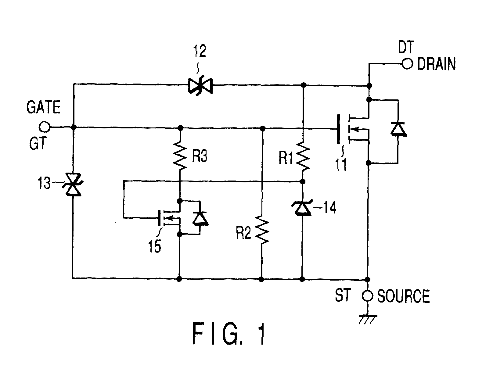
- FIG. 1 is a circuit diagram showing an arrangement of a power semiconductor device according to the embodiment of the present invention.
- This power semiconductor device comprises an n-channel power MOSFET 11, active clamping diode 12, gate protection diode 13, Zener diode 14, lateral type n-channel MOS field effect transistor (hereinafter referred to an n MOS transistor) 15 and resistors R1, R2, and R3.
- n MOS transistor lateral type n-channel MOS field effect transistor
- a drain terminal DT is connected to the drain of the MOSFET 11
- a gate terminal GT is connected to the gate of the MOSFET 11
- a source terminal ST is connected to the source of the MOSFET 11.
- the active clamping diode 12 is connected between the drain terminal DT and the gate terminal GT.
- the resistor Rl and Zener diode 14 are series-connected between the drain terminal DT and the source terminal ST.
- the resistor R2 is connected between the gate terminal GT and the source terminal ST.
- the resistor R3 and n MOS transistor 15 are series-connected between the gate terminal GT and the source terminal ST.
- the gate protection diode 13 is connected between the gate terminal GT and the source terminal ST.
- a resistive value of the resistor R1 is about 1 M ⁇
- a resistive value of the resistor R2 is about 2 M ⁇
- a resistive value of the resistor R3 is about 20 k ⁇ to 100 k ⁇ .
- a variable resistance means is connected to the gate to set the gate-to-source resistive value of the MOSFET 11 variable.
- a current of 7 ⁇ A flows through the resistor R1 and Zener diode 14.
- the resistive value of the resistor R1 is about 1 M ⁇ and that the breakdown voltage (VZ) of the Zener diode 14 is 7V.
- a voltage of 7V is generated at the junction between the resistor R1 and the Zener diode 14.
- the n MOS transistor 15 When the voltage on the above-mentioned junction is applied to the gate of the n MOS transistor 15, the n MOS transistor 15 is turned ON because the threshold voltage of the n MOS transistor 15 is lower than 7V. By doing so, a current flows through the resistor R3 connected between the gate terminal GT and the source terminal ST.
- the resistive value of the resistor R3 is about 20 k ⁇ to 100 k ⁇ and low. For this reason, the gate potential of the MOSFET 11 is lowered so that the gate potential is fixed to below the threshold voltage of the MOSFET 11. In the case where the gate of the MOSFET 11 is brought to the floating state, it is possible to prevent the MOSFET 11 from being turned ON due to a very small current.
- the MOSFET 11 When the gate potential is above the threshold voltage of the MOSFET 11, a current flows through a resistor R2 connected between the gate terminal GT and the source terminal ST.
- the resistive value of the resistor R2 is 2 M ⁇ and high. For this reason, the gate potential of the MOSFET 11 is not lowered and is fixed to a voltage higher than the threshold voltage. By doing so, in the case where the gate potential of the MOSFET 11 is controlled to turn the MOSFET 11 ON, the MOSFET 11 can be turned ON by a very small current.
- a circuit of a simpler arrangement is incorporated into a power MOSFET-equipped semiconductor device without largely increasing the number of component parts and without adopting any IPD, IPM, etc., involving a high cost.
- the power MOSFET can be prevented from being thermally destroyed in the case where the gate potential of the power MOSFET is brought to a not-fixed state.
- FIG. 2 is a cross-sectional view showing a structure model of the MOSFET 11 and n MOS transistor 15.
- the MOSFET 11 use is made of a trench type.
- an n - type epitaxial layer 22 is formed on one surface of an n + type semiconductor substrate 21.
- a p type base layer 23 is formed on the n - type epitaxial layer 22.
- a trench is formed in the n - type epitaxial layer 22 and p type base layer 23.
- a gate insulating film 24 and gate 25 are formed in the trench.
- a gate terminal GT is connected to the gate 25.
- a silicon oxide film is used as the gate insulating film 24 and a polysilicon is used as the gate 25.
- n + type source layers 26 are formed in the p type base layer 23 in the neighborhood of the gate insulating film 24 at an area sandwiched between the two gates 25.
- a source electrode 27 is formed on the n + type source layers 26.
- a grounded source terminal ST is connected to the source electrode 27.
- the source electrode 27 use is made of a metal such as Al.
- the structure as set out above constitutes the MOSFET 11.
- the above-mentioned lateral type n MOS transistor 15 has the following structure.
- a silicon oxide film (such as SiO 2 ) 28 is formed on the p type base layer 23.
- An n + type drain layer 29, n + type source layer 30 and p - type layer 31 are formed on the silicon oxide film 28.
- As the n + type drain layer 29, n + type source layer 30 and p - type layer 31 use is made of polysilicon.
- a drain electrode 32 is formed on the n + type drain electrode 29. One end of a resistor R3 is connected to the drain electrode 32.
- a source electrode 33 is formed on the n + type source layer 30.
- a source terminal ST is connected to the source electrode 33.
- the drain electrode 32 and source electrode 33 for example, use is made of a metal such as Al.
- a gate insulating film (such as SiO 2 ) 34 is formed on the p - type layer 31 and a gate electrode 35 is formed on the gate insulating film 34.
- a junction between the resistor R1 and the Zener diode 14 is connected to the gate electrode 35.
- As the gate electrode 35 for example, use is made of a metal such as aluminum.
- a drain terminal DT is connected to the n + type semiconductor substrate 21. The other connection is the same as that as shown in FIG. 1.
- the lateral type n MOS transistor 15 for switching a resistive value of a variable resistance circuit is provided between the gate and the source of the power MOSFET 11.
- a semiconductor layer (active layer) for creating a channel of the n MOS transistor 15 is formed using a polysilicon (p - type layer 31) on the silicon oxide film 28. This arrangement obviates the necessity of using the element isolation technique, etc., and ensures a simpler circuit structure.
- the present invention is characterized by the variable resistance circuit which makes the gate-to-source resistance value smaller when a voltage applied to the gate of the power transistor is below the threshold voltage and makes the gate-to-source resistance value larger when the voltage applied to the above-mentioned gate is higher than the threshold voltage.
- variable resistance circuit functions as a protection circuit for preventing the power transistor from being destroyed.
- the lateral type n MOS transistor that is, a transistor for a switch for switching a resistive value of the variable resistance circuit, with the use of a polysilicon, it is possible to simplify the structure of this variable resistance circuit.
- a circuit of a simpler structure is incorporated into a power MOSFET-equipped semiconductor structure and, by doing so, it is possible to provide a semiconductor device having a power MOSFET which can prevent the power MOSFET from being thermally destroyed when the gate potential of the power MOSFET is brought to a not-fixed state.
Landscapes
- Metal-Oxide And Bipolar Metal-Oxide Semiconductor Integrated Circuits (AREA)
- Semiconductor Integrated Circuits (AREA)
- Electronic Switches (AREA)
- Insulated Gate Type Field-Effect Transistor (AREA)
- Thin Film Transistor (AREA)
Abstract
Description
Claims (10)
- A power semiconductor device characterized by comprising:a voltage drive type power MOS transistor (11) having a gate, source and drain;a series connection of a first transistor (R1) and Zener diode (14) across which a drain-to-source voltage of the power MOS transistor (11) is applied;a second resistor (R2) across which a gate-to-source voltage of the power MOS transistor (11) is applied; anda series connection of a third resistor (R3) and MOS transistor (15) across which the gate-to-source voltage of the power MOS transistor (11) is applied, the MOS transistor (15) having a gate, source and drain, and the gate of the MOS transistor (15) being connected to a node between the first resistor (R1) and the Zener diode(14).
- A power semiconductor device according to claim 1, characterized in that the third resistor (R3) is lower in resistive level than the second resistor (R2).
- A power semiconductor device according to claim 1, characterized by further comprising a gate protection diode (13) across which the gate-to-source voltage of the power MOS transistor (11) is applied.
- A power semiconductor device characterized by comprising:a voltage drive type power MOS transistor (11) having a gate, source and drain and formed on a semiconductor substrate (21);a series connection of a first resistor (R1) and Zener diode (14) across which a drain-to-source voltage of the power MOS transistor (11) is applied, the first resistor (R1) and Zener diode (14) being formed on the semiconductor substrate;a second resistor (R2) across which a gate-to-source voltage of the power MOS transistor (11) is applied, the second resistor (R2) being formed on the semiconductor substrate; anda series connection of a third resistor (R3) and MOS transistor (15) across which the gate-to-source voltage of the power MOS transistor (11) is applied, the MOS transistor (15) having a gate, source and drain, the gate of the MOS transistor (15) being connected to a node between the first resistor (R1) and the Zener diode (14), and the third resistor (R3) and MOS transistor (15) being formed on the semiconductor substrate (21).
- A power semiconductor device according to claim 4, characterized in that the third resistor (R3) is lower in resistive level than the second resistor (R2).
- A power semiconductor device according to claim 4, characterized by further comprising a gate protection diode (13) across which the gate-to-source voltage of the power MOS transistor (11) is applied.
- A power semiconductor device according to claim 4, characterized in that said power MOS transistor (11) is comprised of a vertical type transistor having its drain and source arranged in a vertical direction relative to the semiconductor substrate and said MOS transistor (15) is comprised of a lateral type transistor having its drain and source arranged in a horizontal direction relative to the semiconductor substrate (21).
- A power semiconductor device according to claim 7, characterized in that a semiconductor layer where a channel of said MOS transistor (15) is created is formed of a polysilicon.
- A power semiconductor device according to claim 8, characterized in that said polysilicon is formed on a surface of an insulating film (28).
- A power semiconductor device according to claim 9, characterized in that said insulating film (28) is formed of a silicon oxide film.
Applications Claiming Priority (2)
| Application Number | Priority Date | Filing Date | Title |
|---|---|---|---|
| JP2000085422 | 2000-03-24 | ||
| JP2000085422A JP2001274402A (en) | 2000-03-24 | 2000-03-24 | Power semiconductor device |
Publications (3)
| Publication Number | Publication Date |
|---|---|
| EP1137068A2 true EP1137068A2 (en) | 2001-09-26 |
| EP1137068A3 EP1137068A3 (en) | 2006-06-28 |
| EP1137068B1 EP1137068B1 (en) | 2008-05-07 |
Family
ID=18601762
Family Applications (1)
| Application Number | Title | Priority Date | Filing Date |
|---|---|---|---|
| EP01106461A Expired - Lifetime EP1137068B1 (en) | 2000-03-24 | 2001-03-23 | Power semiconductor device having a protection circuit |
Country Status (7)
| Country | Link |
|---|---|
| US (1) | US6507088B2 (en) |
| EP (1) | EP1137068B1 (en) |
| JP (1) | JP2001274402A (en) |
| KR (1) | KR100362218B1 (en) |
| CN (1) | CN1162910C (en) |
| DE (1) | DE60133851D1 (en) |
| TW (1) | TW478027B (en) |
Families Citing this family (15)
| Publication number | Priority date | Publication date | Assignee | Title |
|---|---|---|---|---|
| JP4946123B2 (en) * | 2006-03-27 | 2012-06-06 | セイコーエプソン株式会社 | Semiconductor device, electro-optical device and electronic apparatus |
| US7511357B2 (en) * | 2007-04-20 | 2009-03-31 | Force-Mos Technology Corporation | Trenched MOSFETs with improved gate-drain (GD) clamp diodes |
| WO2009128942A1 (en) * | 2008-04-16 | 2009-10-22 | Bourns, Inc. | Current limiting surge protection device |
| US8068322B2 (en) * | 2008-07-31 | 2011-11-29 | Honeywell International Inc. | Electronic circuit breaker apparatus and systems |
| CN101814527A (en) * | 2010-04-22 | 2010-08-25 | 复旦大学 | Power device and method for performing conductivity modulation by using photoelectron injection |
| CN102158228A (en) * | 2011-04-19 | 2011-08-17 | 复旦大学 | Very low voltage millimeter wave injection-locked dichotomous frequency divider |
| JP5959162B2 (en) * | 2011-06-09 | 2016-08-02 | ルネサスエレクトロニクス株式会社 | Semiconductor device and manufacturing method of semiconductor device |
| JP2013065759A (en) * | 2011-09-20 | 2013-04-11 | Toshiba Corp | Semiconductor device |
| JP6056299B2 (en) * | 2012-09-13 | 2017-01-11 | 富士電機株式会社 | Semiconductor device and wire open defect detection method |
| US8816725B2 (en) * | 2012-12-31 | 2014-08-26 | Nxp B.V. | High-voltage electrical switch by series connected semiconductor switches |
| JP2014216573A (en) | 2013-04-26 | 2014-11-17 | 株式会社東芝 | Semiconductor device |
| JP6218462B2 (en) * | 2013-07-04 | 2017-10-25 | 三菱電機株式会社 | Wide gap semiconductor device |
| US10468485B2 (en) | 2017-05-26 | 2019-11-05 | Allegro Microsystems, Llc | Metal-oxide semiconductor (MOS) device structure based on a poly-filled trench isolation region |
| JP7295047B2 (en) * | 2020-01-22 | 2023-06-20 | 株式会社東芝 | semiconductor equipment |
| CN112383293B (en) * | 2020-11-30 | 2024-07-19 | 上海维安半导体有限公司 | Control circuit and chip of intelligent low-side power switch |
Family Cites Families (23)
| Publication number | Priority date | Publication date | Assignee | Title |
|---|---|---|---|---|
| DE1764234A1 (en) * | 1968-04-27 | 1971-07-01 | Bosch Gmbh Robert | Monolithic semiconductor arrangement with integrated power transistors, especially as a voltage regulator for vehicle alternators |
| US4404477A (en) * | 1978-02-22 | 1983-09-13 | Supertex, Inc. | Detection circuit and structure therefor |
| EP0090280A3 (en) * | 1982-03-25 | 1986-03-19 | Nissan Motor Co., Ltd. | Semiconductor integrated circuit device and method of making the same |
| JPH0666472B2 (en) * | 1987-06-22 | 1994-08-24 | 日産自動車株式会社 | MOSFET with overcurrent protection function |
| JPH0749805Y2 (en) * | 1988-06-30 | 1995-11-13 | 関西日本電気株式会社 | Semiconductor device |
| IT1226557B (en) * | 1988-07-29 | 1991-01-24 | Sgs Thomson Microelectronics | CIRCUIT FOR CHECKING THE LOCKING VOLTAGE OF AN INDUCTIVE LOAD DRIVEN WITH A POWER DEVICE IN "HIGH SIDE DRIVER" CONFIGURATION |
| US5172290A (en) | 1988-08-10 | 1992-12-15 | Siemens Aktiengesellschaft | Gate-source protective circuit for a power mosfet |
| US5079608A (en) * | 1990-11-06 | 1992-01-07 | Harris Corporation | Power MOSFET transistor circuit with active clamp |
| DE4120394A1 (en) * | 1991-06-20 | 1992-12-24 | Bosch Gmbh Robert | MONOLITHICALLY INTEGRATED CIRCUIT ARRANGEMENT |
| JP2777307B2 (en) * | 1992-04-28 | 1998-07-16 | 株式会社東芝 | Short circuit protection circuit |
| JP3161092B2 (en) * | 1992-11-05 | 2001-04-25 | 富士電機株式会社 | Dual gate MOS thyristor |
| EP0631390B1 (en) * | 1993-06-22 | 1999-09-01 | Philips Electronics Uk Limited | A power semiconductor circuit |
| JPH07183781A (en) * | 1993-12-22 | 1995-07-21 | Fuji Electric Co Ltd | Semiconductor device and its driving device |
| JP3193827B2 (en) * | 1994-04-28 | 2001-07-30 | 三菱電機株式会社 | Semiconductor power module and power converter |
| GB9423076D0 (en) | 1994-10-12 | 1995-01-04 | Philips Electronics Uk Ltd | A protected switch |
| JPH0918001A (en) | 1995-06-26 | 1997-01-17 | Ricoh Co Ltd | Vertical power MOSFET and manufacturing method thereof |
| JP3495847B2 (en) * | 1995-09-11 | 2004-02-09 | シャープ株式会社 | Semiconductor integrated circuit with thyristor |
| EP0766395A3 (en) * | 1995-09-27 | 1999-04-21 | Siemens Aktiengesellschaft | Power transistor with short-circuit protection |
| US5726594A (en) * | 1995-10-02 | 1998-03-10 | Siliconix Incorporated | Switching device including power MOSFET with internal power supply circuit |
| JP3036423B2 (en) * | 1996-02-06 | 2000-04-24 | 日本電気株式会社 | Semiconductor device |
| US6127746A (en) * | 1996-10-21 | 2000-10-03 | International Rectifier Corp. | Method of controlling the switching DI/DT and DV/DT of a MOS-gated power transistor |
| JP4156717B2 (en) * | 1998-01-13 | 2008-09-24 | 三菱電機株式会社 | Semiconductor device |
| JP2982785B2 (en) * | 1998-04-03 | 1999-11-29 | 富士電機株式会社 | Depletion type MOS semiconductor device and MOS power IC |
-
2000
- 2000-03-24 JP JP2000085422A patent/JP2001274402A/en active Pending
-
2001
- 2001-03-14 TW TW090105993A patent/TW478027B/en not_active IP Right Cessation
- 2001-03-16 KR KR1020010013614A patent/KR100362218B1/en not_active Expired - Fee Related
- 2001-03-20 US US09/811,452 patent/US6507088B2/en not_active Expired - Fee Related
- 2001-03-22 CN CNB011118717A patent/CN1162910C/en not_active Expired - Fee Related
- 2001-03-23 DE DE60133851T patent/DE60133851D1/en not_active Expired - Lifetime
- 2001-03-23 EP EP01106461A patent/EP1137068B1/en not_active Expired - Lifetime
Also Published As
| Publication number | Publication date |
|---|---|
| CN1162910C (en) | 2004-08-18 |
| KR20010093047A (en) | 2001-10-27 |
| KR100362218B1 (en) | 2002-11-23 |
| EP1137068A3 (en) | 2006-06-28 |
| CN1315746A (en) | 2001-10-03 |
| JP2001274402A (en) | 2001-10-05 |
| US20010023967A1 (en) | 2001-09-27 |
| US6507088B2 (en) | 2003-01-14 |
| TW478027B (en) | 2002-03-01 |
| EP1137068B1 (en) | 2008-05-07 |
| DE60133851D1 (en) | 2008-06-19 |
Similar Documents
| Publication | Publication Date | Title |
|---|---|---|
| CN108702147B (en) | Protection circuit, operation method of protection circuit, and semiconductor integrated circuit device | |
| JP3610890B2 (en) | Electric load drive circuit | |
| EP1137068B1 (en) | Power semiconductor device having a protection circuit | |
| JP5383426B2 (en) | Rapid discharge circuit when abnormality is detected | |
| JP3164065B2 (en) | Semiconductor device | |
| EP0733283B1 (en) | A protected switch | |
| CN107527904A (en) | Conductor integrated circuit device | |
| JP4438608B2 (en) | H-bridge circuit drive device and H-bridge circuit protection method | |
| US7916439B2 (en) | Semiconductor switch arrangement and an electronic device | |
| US6441679B1 (en) | Semiconductor active fuse operating at higher supply voltage employing current oscillation | |
| US6597550B1 (en) | High voltage integrated circuit with resistor connected between substrate and ground to limit current during negative voltage spike | |
| US6348820B1 (en) | High-side, low-side configurable driver | |
| US6778366B2 (en) | Current limiting protection circuit | |
| JP4501178B2 (en) | Protective device for semiconductor device | |
| US5466952A (en) | Semiconductor device having an IGET and a control or protection component | |
| EP1139566A1 (en) | Semiconductor circuit with insulated gate device and associated control circuitry | |
| JP2870558B2 (en) | Automotive power integrated circuits | |
| JP3660186B2 (en) | Semiconductor device | |
| JPH0918004A (en) | Semiconductor integrated circuit | |
| JP3698323B2 (en) | Power switch circuit | |
| JPH01262667A (en) | Semiconductor device having protective function | |
| JP2000236022A (en) | Fuse trimming circuit | |
| US20090302397A1 (en) | Field-Effect Transistor | |
| US20080116519A1 (en) | Integrated Circuit Used in Smart Power Technology | |
| MATSUSHITA et al. | Durable and low power-loss semiconductor devices for specific automotive applications |
Legal Events
| Date | Code | Title | Description |
|---|---|---|---|
| PUAI | Public reference made under article 153(3) epc to a published international application that has entered the european phase |
Free format text: ORIGINAL CODE: 0009012 |
|
| 17P | Request for examination filed |
Effective date: 20010323 |
|
| AK | Designated contracting states |
Kind code of ref document: A2 Designated state(s): AT BE CH CY DE DK ES FI FR GB GR IE IT LI LU MC NL PT SE TR |
|
| AX | Request for extension of the european patent |
Free format text: AL;LT;LV;MK;RO;SI |
|
| PUAL | Search report despatched |
Free format text: ORIGINAL CODE: 0009013 |
|
| AK | Designated contracting states |
Kind code of ref document: A3 Designated state(s): AT BE CH CY DE DK ES FI FR GB GR IE IT LI LU MC NL PT SE TR |
|
| AX | Request for extension of the european patent |
Extension state: AL LT LV MK RO SI |
|
| 17Q | First examination report despatched |
Effective date: 20061013 |
|
| AKX | Designation fees paid |
Designated state(s): DE FR GB |
|
| GRAP | Despatch of communication of intention to grant a patent |
Free format text: ORIGINAL CODE: EPIDOSNIGR1 |
|
| GRAS | Grant fee paid |
Free format text: ORIGINAL CODE: EPIDOSNIGR3 |
|
| GRAA | (expected) grant |
Free format text: ORIGINAL CODE: 0009210 |
|
| AK | Designated contracting states |
Kind code of ref document: B1 Designated state(s): DE FR GB |
|
| REG | Reference to a national code |
Ref country code: GB Ref legal event code: FG4D |
|
| RIN1 | Information on inventor provided before grant (corrected) |
Inventor name: YONEDA, TATSUOC/O INT.PROP.DIV.K.K.TOSHIBA |
|
| REF | Corresponds to: |
Ref document number: 60133851 Country of ref document: DE Date of ref document: 20080619 Kind code of ref document: P |
|
| PLBE | No opposition filed within time limit |
Free format text: ORIGINAL CODE: 0009261 |
|
| STAA | Information on the status of an ep patent application or granted ep patent |
Free format text: STATUS: NO OPPOSITION FILED WITHIN TIME LIMIT |
|
| 26N | No opposition filed |
Effective date: 20090210 |
|
| REG | Reference to a national code |
Ref country code: FR Ref legal event code: ST Effective date: 20091130 |
|
| PG25 | Lapsed in a contracting state [announced via postgrant information from national office to epo] |
Ref country code: FR Free format text: LAPSE BECAUSE OF NON-PAYMENT OF DUE FEES Effective date: 20091123 |
|
| PGFP | Annual fee paid to national office [announced via postgrant information from national office to epo] |
Ref country code: GB Payment date: 20120321 Year of fee payment: 12 |
|
| PGFP | Annual fee paid to national office [announced via postgrant information from national office to epo] |
Ref country code: DE Payment date: 20120411 Year of fee payment: 12 |
|
| GBPC | Gb: european patent ceased through non-payment of renewal fee |
Effective date: 20130323 |
|
| REG | Reference to a national code |
Ref country code: DE Ref legal event code: R119 Ref document number: 60133851 Country of ref document: DE Effective date: 20131001 |
|
| PG25 | Lapsed in a contracting state [announced via postgrant information from national office to epo] |
Ref country code: GB Free format text: LAPSE BECAUSE OF NON-PAYMENT OF DUE FEES Effective date: 20130323 Ref country code: DE Free format text: LAPSE BECAUSE OF NON-PAYMENT OF DUE FEES Effective date: 20131001 |