EP1134797A2 - Bipolar transistor having recessed and rounded surface and its manufacturing method - Google Patents
Bipolar transistor having recessed and rounded surface and its manufacturing method Download PDFInfo
- Publication number
- EP1134797A2 EP1134797A2 EP01104417A EP01104417A EP1134797A2 EP 1134797 A2 EP1134797 A2 EP 1134797A2 EP 01104417 A EP01104417 A EP 01104417A EP 01104417 A EP01104417 A EP 01104417A EP 1134797 A2 EP1134797 A2 EP 1134797A2
- Authority
- EP
- European Patent Office
- Prior art keywords
- semiconductor substrate
- layer
- base region
- recessed
- conductive layer
- Prior art date
- Legal status (The legal status is an assumption and is not a legal conclusion. Google has not performed a legal analysis and makes no representation as to the accuracy of the status listed.)
- Withdrawn
Links
- 238000004519 manufacturing process Methods 0.000 title claims description 11
- 239000000758 substrate Substances 0.000 claims abstract description 67
- 239000004065 semiconductor Substances 0.000 claims abstract description 38
- 238000000034 method Methods 0.000 claims description 58
- 239000012535 impurity Substances 0.000 claims description 10
- 238000000137 annealing Methods 0.000 claims description 7
- 238000005530 etching Methods 0.000 claims description 7
- 238000001020 plasma etching Methods 0.000 claims description 6
- 238000000059 patterning Methods 0.000 claims 1
- 229910021420 polycrystalline silicon Inorganic materials 0.000 description 50
- 229910021421 monocrystalline silicon Inorganic materials 0.000 description 29
- 229910052581 Si3N4 Inorganic materials 0.000 description 19
- HQVNEWCFYHHQES-UHFFFAOYSA-N silicon nitride Chemical compound N12[Si]34N5[Si]62N3[Si]51N64 HQVNEWCFYHHQES-UHFFFAOYSA-N 0.000 description 19
- VYPSYNLAJGMNEJ-UHFFFAOYSA-N Silicium dioxide Chemical compound O=[Si]=O VYPSYNLAJGMNEJ-UHFFFAOYSA-N 0.000 description 18
- 229910052814 silicon oxide Inorganic materials 0.000 description 18
- 238000005229 chemical vapour deposition Methods 0.000 description 15
- 230000015556 catabolic process Effects 0.000 description 13
- 229920002120 photoresistant polymer Polymers 0.000 description 9
- -1 boron ions Chemical class 0.000 description 8
- 238000001039 wet etching Methods 0.000 description 7
- 229910052796 boron Inorganic materials 0.000 description 6
- 230000003247 decreasing effect Effects 0.000 description 4
- 238000001312 dry etching Methods 0.000 description 4
- 238000000206 photolithography Methods 0.000 description 4
- 238000003780 insertion Methods 0.000 description 3
- 230000037431 insertion Effects 0.000 description 3
- 230000003647 oxidation Effects 0.000 description 3
- 238000007254 oxidation reaction Methods 0.000 description 3
- 229910052785 arsenic Inorganic materials 0.000 description 2
- 230000001419 dependent effect Effects 0.000 description 2
- 238000009792 diffusion process Methods 0.000 description 2
- 238000002955 isolation Methods 0.000 description 2
- KRHYYFGTRYWZRS-UHFFFAOYSA-N Fluorane Chemical compound F KRHYYFGTRYWZRS-UHFFFAOYSA-N 0.000 description 1
- 239000011521 glass Substances 0.000 description 1
- 229910000040 hydrogen fluoride Inorganic materials 0.000 description 1
- 230000001590 oxidative effect Effects 0.000 description 1
- 239000007790 solid phase Substances 0.000 description 1
- 239000012808 vapor phase Substances 0.000 description 1
Images






Classifications
-
- H—ELECTRICITY
- H10—SEMICONDUCTOR DEVICES; ELECTRIC SOLID-STATE DEVICES NOT OTHERWISE PROVIDED FOR
- H10D—INORGANIC ELECTRIC SEMICONDUCTOR DEVICES
- H10D10/00—Bipolar junction transistors [BJT]
- H10D10/01—Manufacture or treatment
- H10D10/051—Manufacture or treatment of vertical BJTs
-
- H—ELECTRICITY
- H10—SEMICONDUCTOR DEVICES; ELECTRIC SOLID-STATE DEVICES NOT OTHERWISE PROVIDED FOR
- H10D—INORGANIC ELECTRIC SEMICONDUCTOR DEVICES
- H10D10/00—Bipolar junction transistors [BJT]
- H10D10/40—Vertical BJTs
- H10D10/421—Vertical BJTs having both emitter-base and base-collector junctions ending at the same surface of the body
-
- H—ELECTRICITY
- H10—SEMICONDUCTOR DEVICES; ELECTRIC SOLID-STATE DEVICES NOT OTHERWISE PROVIDED FOR
- H10D—INORGANIC ELECTRIC SEMICONDUCTOR DEVICES
- H10D62/00—Semiconductor bodies, or regions thereof, of devices having potential barriers
- H10D62/10—Shapes, relative sizes or dispositions of the regions of the semiconductor bodies; Shapes of the semiconductor bodies
- H10D62/17—Semiconductor regions connected to electrodes not carrying current to be rectified, amplified or switched, e.g. channel regions
- H10D62/177—Base regions of bipolar transistors, e.g. BJTs or IGBTs
Definitions
- the present invention relates to a bipolar transistor and its manufacturing method.
- a first insulating layer, a first polycrystalline silicon layer of a second conductivity type and a second insulating layer are sequentially formed on a semiconductor substrate of a first conductivity type. Then, the second insulating layer and the first polycrystalline silicon layer are patterned to form an opening therein. Then, the first insulating layer is overetched by using the second insulating layer and the first polycrystalline silicon layer as a mask. Then, a second polycrystalline silicon layer is formed on the entire surface.
- an oxidizing process is performed upon the second polycrystalline silicon layer except for a part of the second polycrystalline silicon layer under the first polycrystalline silicon layer, and the oxidized part of the second polycrystalline silicon layer is removed by a wet etching process.
- impurities of the second conductivity type are implanted into the semiconductor substrate to form a base region.
- a sidewall insulating layer is formed on a sidewall of the first and second polycrystalline silicon layers.
- a third polycrystalline silicon layer of the first conductivity type is formed on the base region. Finally, an annealing operation is carried out.
- impurities of the second conductivity type are diffused from the first polycrystalline silicon layer via the second polycrystalline silicon layer into the semiconductor substrate to form a graft base region, and impurities of the first conductivity type are diffused from the third polycrystalline silicon layer into the base region to form an emitter region.
- the semiconductor substrate is hardly etched at the wet etching process for etching the second polycrystalline silicon layer, the transistor characteristics are hardly deteriorated (see JP-A-11-283991 & U.S.Patent No. 6124181). This will be explained later in detail.
- the base region is formed by implanting impurities into the semiconductor substrate whose surface is flat, the base region is sharply edged.
- a base-to-collector current is focused on the edged portions, so that the base-to-collector breakdown voltage is mainly dependent upon the current flowing through the edged portions, to decrease the base-to-collector breakdown voltage.
- the bipolar transistor is more-fined, the base-to-collector breakdown voltage is remarkably decreased.
- a bipolar transistor is constructed by a semiconductor substrate having a recessed and rounded surface, a collector region formed in the semiconductor substrate, a base region formed in the semiconductor substrate in contact with the collector region and having a configuration along the recessed and rounded surface, an emitter region formed between the recessed and round surface and the base region, and a graft base region formed in the semiconductor substrate in contact with the base region at an outer portion of the recessed and rounded surface.
- an isotropic microwave plasma etching process is performed upon the second conductive layer and the semiconductor substrate so that the second conductive layer is left only on sidewalls of the first insulating layer and an exposed surface of the semiconductor substrate is recessed and rounded.
- impurities of the second conductivity type are implanted into the semiconductor substrate to form a base region in the semiconductor substrate.
- a third insulating layer is formed on sidewalls of the second insulating layer and the first and second conductive layers.
- a third conductive layer of the first conductivity type is formed on the base region in contact with the third insulating layer.
- an annealing operation is carried out.
- impurities of the second conductivity type are diffused from the first conductive layer via the second conductive layer into the semiconductor substrate to form a graft base region in the semiconductor substrate in contact with the base region, and impurities of the first conductivity type are diffused from the third conductive layer into the base region to form an emitter region in the base region.
- a photoresist pattern layer 5 is formed on the silicon nitride layer 4 by a photolithography process. Then, the silicon nitride layer 4 and the boron-doped polycrystalline silicon layer 3 are etched by an anistopic dry etching process using the photoresist pattern layer 5 as a mask. Then, an opening is perforated in the silicon nitride layer 4 and the boron-doped polycrystalline silicon layer 3.
- the silicon oxide layer 2 is side-etched by an isotropic ethcing process, i.e., a wet etching process using the photoresist pattern layer 5, the silicon nitride layer 4 and the boron-doped polycrystalline silicon layer 3 as a mask. Then, the photoresist pattern layer 5 is removed.
- an isotropic ethcing process i.e., a wet etching process using the photoresist pattern layer 5, the silicon nitride layer 4 and the boron-doped polycrystalline silicon layer 3 as a mask.
- the silicon oxide layer 6a is etched by a wet etching process using hydrogen fluoride and using the silicon nitride layer 4 as a mask.
- the non-doped polycrystalline silicon layer 6 is left only on the sidewalls of the silicon oxide layer 6, so that the boron-doped polycrystalline silicon layer 3 is connected via the non-doped polycrystalline silicon layer 6 to the monocrystalline silicon substrate.
- the monocrystalline silicon substrate 1 is hardly etched, so that the surface thereof is flat.
- Figs. 1E and IF although the non-doped polycrystalline silicon layer 6 is oxidized, an anisotropic plasma etching process can be performed directly upon the non-doped polycrystalline silicon layer 6, so that the non-doped polycrystalline silicon layer 6 is left only on the sidewalls of the silicon oxide layer 6. Even in this case, the surface of the monocrystalline silicon substrate 1 is flat.
- a silicon nitride layer 9 is deposited on the entire surface by a CVD process.
- the silicon nitride layer 9 is etched back by an anisotropic dry etching process, and then, the silicon oxide layer 7 is etched by a wet etching process.
- a sidewall insulating layer serving as an isolation region between a base lead-out portion and an emitter lead-out portion is formed by the silicon oxide layer 7 and the silicon nitride layer 9.
- an arsenic-doped polycrystalline silicon layer 10 is deposited on the entire surface by a CVD process. Then, the arsenic-doped polycrystalline silicon layer is patterned by a photolithography and etching process.
- an insulating layer 11 made of phospho-silicated glass (PSG) or the like is deposited on the entire surface by a CVD process.
- an annealing operation is carried out.
- boron ions are diffused from the boron-doped polycrystalline silicon layer 3 via the non-doped polycrystalline silicon layer 6 into the monocrystalline silicon substrate 1, to form a P + -type graft base region 12 within the monocrystalline silicon substrate.
- the P-type base region 8 per se is expanded by the annealing operation, so that the P-type base region 8 is in contact with the P + -type graft base region 12.
- the edged portions X remain in the P-type base region 8.
- arsenic ions are diffused from the arsenic-doped polycrystalline silicon layer 10 into the monocrystalline silicon substrate 1, to form an N-type emitter region 13 within the P-type base region 8.
- a vertical NPN-type bipolar transistor having the monocrystalline silicon substrate 1 as a collector connected to a collector electrode (not shown) is completed.
- the P-type base region 8 is formed by implanting boron ions into the monocrystalline silicon substrate 1 whose surface is flat, the P-type base region 8 is edged as indicated by arrows X in Fig. 1M.
- a base-to-collector current is focused on the edged portions X, so that the base-to-collector breakdown voltage is mainly dependent upon the current flowing through the edged portions X, to decrease the base-to-collector breakdown voltage.
- the bipolar transistor is more-fined, the base-to-collector breakdown voltage is remarkably decreased.
- the silicon nitride layer 4 and the boron-doped polycrystalline silicon layer 3 are etched by an anisotropic dry etching process using the photoresist pattern layer 5 as a mask. Then, an opening is perforated in the silicon nitride layer 4 and the boron-doped polycrystalline silicon layer 3. Then, the silicon oxide layer 2 is side-etched by an isotropic etching process, i.e., a wet etching process using the photoresist pattern layer 5, the silicon nitride layer 4 and the boron-doped polycrystalline silicon layer 3 as a mask. Then, the photoresist pattern layer 5 is removed. Then, a non-doped polycrystalline silicon layer 6 is deposited on the entire surface by a CVD process.
- an isotropic microwave plasma etching process is performed upon the non-doped polycrystalline silicon layer 6.
- the non-doped polycrystalline silicon layer 6 is left only on the sidewalls of the silicon oxide layer 6, so that the boron-doped polycrystalline silicon layer 3 is connected via the non-doped polycrystalline silicon layer 6 to the monocrystalline silicon substrate.
- the monocrystalline silicon substrate 1 is also etched by the isotropic microwave plasma etching process, so that the surface of the monocrystalline silicon substrate 1 is recessed and rounded, as indicated by an arrow Y.
- the depth "d" of the recessed and rounded portion Y is about 1000 to 1500 ⁇ .
- a silicon oxide layer 7 is deposited on the entire surface by a CVD process.
- boron ions are implanted into the monocrystalline silicon substrate 1 by using the silicon nitride layer 4 and the boron-doped polycrystalline silicon layer 3 as a mask.
- a P-type base layer 8 is formed within the monocrystalline silicon substrate 1.
- the P-type base region 8 is edged as indicated by arrows Z.
- the sharpness of the edged portions Z are alleviated as compared with the edged portions X of Fig. 1G, due to the rounded surface of the monocrystalline silicon substrate 1.
- a silicon nitride layer 9 is deposited on the entire surface by a CVD process.
- the silicon nitride layer 9 is etched back by an anisotropic dry etching process, and then, the silicon oxide layer 7 is etched by a wet etching process.
- a sidewall insulating layer serving as an isolation region between a base lead-out portion and an emitter lead-out portion is formed by the silicon oxide layer 7 and the silicon nitride layer 9.
- an arsenic-doped polycrystalline silicon layer 10 is deposited on the entire surface by a CVD process. Then, the arsenic-doped polycrystalline silicon layer is patterned by a photolithography and etching process.
- an insulating layer 11 made of PSG or the like is deposited on the entire surface by a CVD process.
- annealing operation is carried out.
- boron ions are diffused from the boron-doped polycrystalline silicon layer 3 via the non-doped polycrystalline silicon layer 6 into the monocrystalline silicon substrate 1, to form a P + -type graft base region 12 within the monocrystalline silicon substrate 1.
- the P-type base region 8 per se is expanded by the annealing operation, so that the P-type base region 8 is in contact with the P + -type graft base region 12.
- the edged portions Z of the P-type base region 8 are absorbed into the P + -type graft base region 12.
- arsenic ions are diffused from the arsenic-doped polycrystalline silicon layer 10 into the monocrystalline silicon substrate 1, to form an N-type emitter region 13 within the P-type base region 8.
- a contact hole is perforated in the insulating layer 11, and then, an emitter electrode 14E is formed therein. Also, a base electrode 14B is formed and connected to the P + -type graft base region 12. Further, a collector electrode 15 is formed on the back surface of the monocrystalline silicon substrate 1.
- a vertical NPN-type bipolar transistor having the monocrystalline silicon substrate 1 as a collector connected to a collector electrode (not shown) is completed.
- the P-type base region 8 is formed by implanting boron ions into the monocrystalline silicon substrate 1 whose surface is recessed and rounded, the P-type base region 8 is rounded as illustrated in Fig. 2H.
- a base-to-collector current is not focused on the portions near the P + -type graft base region 12, so that the base-to-collector current is made uniform within the P-type base region 8, to increase the base-to-collector breakdown voltage.
- the base-to-collector breakdown voltage is not decreased.
- Fig. 3 which shows a relationship between the insertion gain G and the depth "d" of the recessed and rounded portion Y of the monocrystalline silicon substrate 1 of Fig. 2A
- the depth "d" is less than about 1500 ⁇
- the insertion gain G is not decreased.
- the depth "d" is more than about 1500 ⁇
- the length of the P-type base region 8 between the P + -type graft base regions 12 is substantially increased, so that the base resistance is increased, which would deteriorate the high frequency characteristics.
- the larger the depth "d” the larger the base-to-collector breakdown voltage.
- the depth "d" is more than about 500 ⁇ , particularly, more than about 1000 ⁇
- the base-to-collector breakdown voltage has been increased, as shown in Fig. 4.
- the depth "d" of the recessed and rounded portion Y of the monocrystalline silicon substrate 1 of Fig. 2A is about 500 ⁇ to 1500 ⁇ , preferably, about 1000 ⁇ to 1500 ⁇ .
- Figs. 5, 6 and 7 are cross-sectional views taken along the lines VI - VI and VII-VII, respectively, of Fig. 5.
- reference numeral 21 designates a P-type monocrystalline silicon substrate
- 22 designates an N + -type buried collector region
- 23 designates an N + -type collector lead-out region.
- the N'-type buried collector region 22 and the N + -type collector lead-out region 23 as well as the N-type monocrystalline silicon substrate 1 can be formed by an epitaxial layer.
- reference numerals 14B and 14C designate a base electrode and a collector electrode, respectively.
- the above-described embodiment is related to a vertical NPN-type bipolar transistor; however, the present invention can be applied to a vertical PNP-type bipolar transistor.
- the base region 8 can be formed by a vapor phase diffusion process, a solid phase diffusion process or an epitaxial growth process.
- the base region is rounded, the base-to-collector breakdown voltage characteristics can be improved.
Landscapes
- Bipolar Transistors (AREA)
Abstract
A bipolar transistor is constructed by a semiconductor
substrate (1) having a recessed and rounded surface (Y), a
collector region formed in the semiconductor substrate, a base
region (8) formed in the semiconductor substrate in contact
with the collector region and having a configuration along the
recessed and rounded surface, an emitter region (13) formed
between the recessed and round surface and the base region,
and a graft base region (12) formed in the semiconductor
substrate in contact with the base region at an outer portion
of the recessed and rounded surface.
Description
- The present invention relates to a bipolar transistor and its manufacturing method.
- In a prior art method for manufacturing a bipolar transistor, a first insulating layer, a first polycrystalline silicon layer of a second conductivity type and a second insulating layer are sequentially formed on a semiconductor substrate of a first conductivity type. Then, the second insulating layer and the first polycrystalline silicon layer are patterned to form an opening therein. Then, the first insulating layer is overetched by using the second insulating layer and the first polycrystalline silicon layer as a mask. Then, a second polycrystalline silicon layer is formed on the entire surface. Then, an oxidizing process is performed upon the second polycrystalline silicon layer except for a part of the second polycrystalline silicon layer under the first polycrystalline silicon layer, and the oxidized part of the second polycrystalline silicon layer is removed by a wet etching process. Then, impurities of the second conductivity type are implanted into the semiconductor substrate to form a base region. Then, a sidewall insulating layer is formed on a sidewall of the first and second polycrystalline silicon layers. Then, a third polycrystalline silicon layer of the first conductivity type is formed on the base region. Finally, an annealing operation is carried out. As a result, impurities of the second conductivity type are diffused from the first polycrystalline silicon layer via the second polycrystalline silicon layer into the semiconductor substrate to form a graft base region, and impurities of the first conductivity type are diffused from the third polycrystalline silicon layer into the base region to form an emitter region. Thus, since the semiconductor substrate is hardly etched at the wet etching process for etching the second polycrystalline silicon layer, the transistor characteristics are hardly deteriorated (see JP-A-11-283991 & U.S.Patent No. 6124181). This will be explained later in detail.
- In the above-described prior art method, since the base region is formed by implanting impurities into the semiconductor substrate whose surface is flat, the base region is sharply edged. As a result, a base-to-collector current is focused on the edged portions, so that the base-to-collector breakdown voltage is mainly dependent upon the current flowing through the edged portions, to decrease the base-to-collector breakdown voltage. Particularly, when the bipolar transistor is more-fined, the base-to-collector breakdown voltage is remarkably decreased.
- It is an object of the present invention to provide a bipolar transistor and its manufacturing method capable of improving the base-to-collector breakdown voltage characteristics.
- According to the present invention, a bipolar transistor is constructed by a semiconductor substrate having a recessed and rounded surface, a collector region formed in the semiconductor substrate, a base region formed in the semiconductor substrate in contact with the collector region and having a configuration along the recessed and rounded surface, an emitter region formed between the recessed and round surface and the base region, and a graft base region formed in the semiconductor substrate in contact with the base region at an outer portion of the recessed and rounded surface.
- Also, in a method for manufacturing a bipolar transistor, a first insulating layer, a first conductive layer of a second conductivity type and a second insulating layer are sequentially formed on a semiconductor substrate of a first conductivity type. Then, the second insulating layer and the first conductive layer are patterned by an anistropic etching process to form an opening in the second insulating layer and the first conductive layer. Then, the first insulating layer is overetched by using the second insulating layer and the first conductive layer. Then, a second conductive layer is formed on an entire exposed surface of the semiconductor substrate, the first and second insulating layers and the first conductive layer. Then, an isotropic microwave plasma etching process is performed upon the second conductive layer and the semiconductor substrate so that the second conductive layer is left only on sidewalls of the first insulating layer and an exposed surface of the semiconductor substrate is recessed and rounded. Then, impurities of the second conductivity type are implanted into the semiconductor substrate to form a base region in the semiconductor substrate. Then, a third insulating layer is formed on sidewalls of the second insulating layer and the first and second conductive layers. Then, a third conductive layer of the first conductivity type is formed on the base region in contact with the third insulating layer. Finally, an annealing operation is carried out. As a result, impurities of the second conductivity type are diffused from the first conductive layer via the second conductive layer into the semiconductor substrate to form a graft base region in the semiconductor substrate in contact with the base region, and impurities of the first conductivity type are diffused from the third conductive layer into the base region to form an emitter region in the base region.
- The present invention will be more clearly understood from the description set forth below, as compared with the prior art, with reference to the accompanying drawings, wherein:
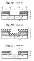
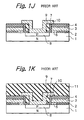
- Figs. 1A through 1M are cross-sectional views for explaining a prior art method for manufacturing a bipolar transistor;
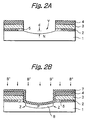
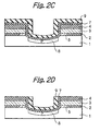
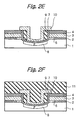
- Figs. 2A through 2H are cross-sectional views for explaining an embodiment of the method for manufacturing a bipolar transistor according to the present invention;
- Fig. 3 is a graph showing a relationship between the insertion gain and the depth of the recessed and rounded portion of Fig. 2H;
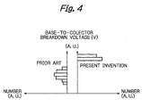
- Fig. 4 is a graph showing the base-to-collector breakdown voltage characteristics of the present invention and the prior art;
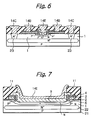
- Fig. 5 is a plan view illustrating a buried collector type bipolar transistor to which the embodiment of the present invention is applied; and
- Figs. 6 and 7 are cross-sectional views taken along the lines VI-VI and VII-VII, respectively, of Fig. 5.
-
- Before the description of the preferred embodiment, a prior art method for manufacturing a bipolar transistor will be explained with reference to Figs. 1A through 1M (see JP-A-11-283991 & U.S.Patent No.6,124,181).
- First, referring to Fig. 1A, an oxidation process is performed upon an N-type
monocrystalline silicon substrate 1 to form asilicon oxide layer 2. Then, a boron-dopedpolycrystalline silicon layer 3 is deposited on thesilicon oxide layer 2 by a chemical vapor deposition (CVD) process. Then, asilicon nitride layer 4 is deposited on the boron-dopedpolycrystalline silicon layer 3 by a CVD process. - Next, referring to Fig. 1B, a
photoresist pattern layer 5 is formed on thesilicon nitride layer 4 by a photolithography process. Then, thesilicon nitride layer 4 and the boron-dopedpolycrystalline silicon layer 3 are etched by an anistopic dry etching process using thephotoresist pattern layer 5 as a mask. Then, an opening is perforated in thesilicon nitride layer 4 and the boron-dopedpolycrystalline silicon layer 3. - Next, referring to Fig. 1C, the
silicon oxide layer 2 is side-etched by an isotropic ethcing process, i.e., a wet etching process using thephotoresist pattern layer 5, thesilicon nitride layer 4 and the boron-dopedpolycrystalline silicon layer 3 as a mask. Then, thephotoresist pattern layer 5 is removed. - Note that the
photoresist pattern layer 5 can be removed before the side-etching of thesilicon oxide layer 2. - Next, referring to Fig. 1D, a non-doped
polycrystalline silicon layer 6 is deposited on the entire surface by a CVD process. - Next, referring to Fig. 1E, an oxidation process is performed upon the non-doped
polycrystalline silicon layer 6. As a result, an exposed portion of the non-dopedpolycrystalline silicon layer 6 is converted into a silicon oxide layer 6a. - Next, referring to Fig. IF, the silicon oxide layer 6a is etched by a wet etching process using hydrogen fluoride and using the
silicon nitride layer 4 as a mask. As a result, the non-dopedpolycrystalline silicon layer 6 is left only on the sidewalls of thesilicon oxide layer 6, so that the boron-dopedpolycrystalline silicon layer 3 is connected via the non-dopedpolycrystalline silicon layer 6 to the monocrystalline silicon substrate. In this case, note that themonocrystalline silicon substrate 1 is hardly etched, so that the surface thereof is flat. - In Figs. 1E and IF, although the non-doped
polycrystalline silicon layer 6 is oxidized, an anisotropic plasma etching process can be performed directly upon the non-dopedpolycrystalline silicon layer 6, so that the non-dopedpolycrystalline silicon layer 6 is left only on the sidewalls of thesilicon oxide layer 6. Even in this case, the surface of themonocrystalline silicon substrate 1 is flat. - Next, referring to Fig. 1G, a
silicon oxide layer 7 is deposited on the entire surface by a CVD process. Then, boron ions are implanted into themonocrystalline silicon substrate 1 by using thesilicon nitride layer 4 and the boron-dopedpolycrystalline silicon layer 3 as a mask. As a result, a P-type base layer 8 is formed within themonocrystalline silicon substrate 1. In this case, the P-type base layer 8 is edged as indicated by arrows X. - Next, referring to Fig. 1H, a
silicon nitride layer 9 is deposited on the entire surface by a CVD process. - Next, referring to Fig. 1I, the
silicon nitride layer 9 is etched back by an anisotropic dry etching process, and then, thesilicon oxide layer 7 is etched by a wet etching process. Thus, a sidewall insulating layer serving as an isolation region between a base lead-out portion and an emitter lead-out portion is formed by thesilicon oxide layer 7 and thesilicon nitride layer 9. - Next, referring to Fig. 1J, an arsenic-doped
polycrystalline silicon layer 10 is deposited on the entire surface by a CVD process. Then, the arsenic-doped polycrystalline silicon layer is patterned by a photolithography and etching process. - Next, referring to Fig. 1K, an insulating
layer 11 made of phospho-silicated glass (PSG) or the like is deposited on the entire surface by a CVD process. - Next, referring to Fig. 1L, an annealing operation is carried out. As a result, boron ions are diffused from the boron-doped
polycrystalline silicon layer 3 via the non-dopedpolycrystalline silicon layer 6 into themonocrystalline silicon substrate 1, to form a P+-typegraft base region 12 within the monocrystalline silicon substrate. In this case, the P-type base region 8 per se is expanded by the annealing operation, so that the P-type base region 8 is in contact with the P+-typegraft base region 12. Note that the edged portions X remain in the P-type base region 8. Simultaneously, arsenic ions are diffused from the arsenic-dopedpolycrystalline silicon layer 10 into themonocrystalline silicon substrate 1, to form an N-type emitter region 13 within the P-type base region 8. - Finally, referring to Fig. 1M, a contact hole is perforated in the insulating
layer 11, and then, anemitter electrode 14E is formed therein. Also, abase electrode 14B is formed and connected to the P'-typegraft base region 12. Further, acollector electrode 15 is formed on the back surface of themonocrystalline silicon substrate 1. - Thus, a vertical NPN-type bipolar transistor having the
monocrystalline silicon substrate 1 as a collector connected to a collector electrode (not shown) is completed. - In the bipolar transistor manufactured by the method as illustrated in Figs. 1A through 1M, since the P-
type base region 8 is formed by implanting boron ions into themonocrystalline silicon substrate 1 whose surface is flat, the P-type base region 8 is edged as indicated by arrows X in Fig. 1M. As a result, a base-to-collector current is focused on the edged portions X, so that the base-to-collector breakdown voltage is mainly dependent upon the current flowing through the edged portions X, to decrease the base-to-collector breakdown voltage. Particularly, when the bipolar transistor is more-fined, the base-to-collector breakdown voltage is remarkably decreased. - An embodiment of the method for manufacturing a bipolar transistor according to the present invention will be explained next with reference to Figs. 2A through 2H.
- First, the manufacturing steps as illustrated in Figs. 1A through 1D are carried out. That is, an oxidation process is performed upon an N-type
monocrystalline silicon substrate 1 to form asilicon oxide layer 2. Then, a boron-dopedpolycrystalline silicon layer 3 is deposited on thesilicon oxide layer 2 by a CVD process. Then, asilicon nitride layer 4 is deposited on the boron-dopedpolycrystalline silicon layer 3 by a CVD process. Then, aphotoresist pattern layer 5 is formed on thesilicon nitride layer 4 by a photolithography process. Then, thesilicon nitride layer 4 and the boron-dopedpolycrystalline silicon layer 3 are etched by an anisotropic dry etching process using thephotoresist pattern layer 5 as a mask. Then, an opening is perforated in thesilicon nitride layer 4 and the boron-dopedpolycrystalline silicon layer 3. Then, thesilicon oxide layer 2 is side-etched by an isotropic etching process, i.e., a wet etching process using thephotoresist pattern layer 5, thesilicon nitride layer 4 and the boron-dopedpolycrystalline silicon layer 3 as a mask. Then, thephotoresist pattern layer 5 is removed. Then, a non-dopedpolycrystalline silicon layer 6 is deposited on the entire surface by a CVD process. - Next, referring to Fig. 2A, an isotropic microwave plasma etching process is performed upon the non-doped
polycrystalline silicon layer 6. As a result, the non-dopedpolycrystalline silicon layer 6 is left only on the sidewalls of thesilicon oxide layer 6, so that the boron-dopedpolycrystalline silicon layer 3 is connected via the non-dopedpolycrystalline silicon layer 6 to the monocrystalline silicon substrate. Simultaneously, themonocrystalline silicon substrate 1 is also etched by the isotropic microwave plasma etching process, so that the surface of themonocrystalline silicon substrate 1 is recessed and rounded, as indicated by an arrow Y. In this case, the depth "d" of the recessed and rounded portion Y is about 1000 to 1500Å. - Next, referring to Fig. 2B, in the same way as in Fig. 1G, a
silicon oxide layer 7 is deposited on the entire surface by a CVD process. Then, boron ions are implanted into themonocrystalline silicon substrate 1 by using thesilicon nitride layer 4 and the boron-dopedpolycrystalline silicon layer 3 as a mask. As a result, a P-type base layer 8 is formed within themonocrystalline silicon substrate 1. Even in this case, the P-type base region 8 is edged as indicated by arrows Z. However, the sharpness of the edged portions Z are alleviated as compared with the edged portions X of Fig. 1G, due to the rounded surface of themonocrystalline silicon substrate 1. - Next, referring to Fig. 2C, in the same way as in Fig. 1H, a
silicon nitride layer 9 is deposited on the entire surface by a CVD process. - Next, referring to Fig. 2D, in the same way as in Fig. 1I, the
silicon nitride layer 9 is etched back by an anisotropic dry etching process, and then, thesilicon oxide layer 7 is etched by a wet etching process. Thus, a sidewall insulating layer serving as an isolation region between a base lead-out portion and an emitter lead-out portion is formed by thesilicon oxide layer 7 and thesilicon nitride layer 9. - Next, referring to Fig. 2E, in the same way as in Fig. 1J, an arsenic-doped
polycrystalline silicon layer 10 is deposited on the entire surface by a CVD process. Then, the arsenic-doped polycrystalline silicon layer is patterned by a photolithography and etching process. - Next, referring to Fig. 2F, in the same way as in Fig. 1K, an insulating
layer 11 made of PSG or the like is deposited on the entire surface by a CVD process. - Next, referring to Fig. 2G, in the same way as in Fig. 1L, an annealing operation is carried out. As a result, boron ions are diffused from the boron-doped
polycrystalline silicon layer 3 via the non-dopedpolycrystalline silicon layer 6 into themonocrystalline silicon substrate 1, to form a P+-typegraft base region 12 within themonocrystalline silicon substrate 1. In this case, the P-type base region 8 per se is expanded by the annealing operation, so that the P-type base region 8 is in contact with the P+-typegraft base region 12. Note that the edged portions Z of the P-type base region 8 are absorbed into the P+-typegraft base region 12. Simultaneously, arsenic ions are diffused from the arsenic-dopedpolycrystalline silicon layer 10 into themonocrystalline silicon substrate 1, to form an N-type emitter region 13 within the P-type base region 8. - Finally, referring to Fig. 2H, in the same way as in Fig. 1M, a contact hole is perforated in the insulating
layer 11, and then, anemitter electrode 14E is formed therein. Also, abase electrode 14B is formed and connected to the P+-typegraft base region 12. Further, acollector electrode 15 is formed on the back surface of themonocrystalline silicon substrate 1. - Thus, a vertical NPN-type bipolar transistor having the
monocrystalline silicon substrate 1 as a collector connected to a collector electrode (not shown) is completed. - In the bipolar transistor manufactured by the method as illustrated in Figs. 2A through 2H as well as Figs. 1A through 1D, since the P-
type base region 8 is formed by implanting boron ions into themonocrystalline silicon substrate 1 whose surface is recessed and rounded, the P-type base region 8 is rounded as illustrated in Fig. 2H. As a result, a base-to-collector current is not focused on the portions near the P+-typegraft base region 12, so that the base-to-collector current is made uniform within the P-type base region 8, to increase the base-to-collector breakdown voltage. Particularly, even when the bipolar transistor is more-fined, the base-to-collector breakdown voltage is not decreased. - In Fig. 3, which shows a relationship between the insertion gain G and the depth "d" of the recessed and rounded portion Y of the
monocrystalline silicon substrate 1 of Fig. 2A, when the depth "d" is less than about 1500Å, the insertion gain G is not decreased. On the other hand, when the depth "d" is more than about 1500Å, the length of the P-type base region 8 between the P+-typegraft base regions 12 is substantially increased, so that the base resistance is increased, which would deteriorate the high frequency characteristics. Note that the larger the depth "d", the larger the base-to-collector breakdown voltage. For example, when the depth "d" is more than about 500Å, particularly, more than about 1000 Å, the base-to-collector breakdown voltage has been increased, as shown in Fig. 4. - In view of the foregoing, the depth "d" of the recessed and rounded portion Y of the
monocrystalline silicon substrate 1 of Fig. 2A is about 500Å to 1500Å, preferably, about 1000Å to 1500Å. - The about-described embodiment is applied to a buried collector type bipolar transistor as illustrated in Figs. 5, 6 and 7. Note that Fig. 5 is a plan view, and Figs. 6 and 7 are cross-sectional views taken along the lines VI - VI and VII-VII, respectively, of Fig. 5. In Figs. 5, 6 and 7,
reference numeral 21 designates a P-type monocrystalline silicon substrate, 22 designates an N+-type buried collector region, and 23 designates an N+-type collector lead-out region. In this case, the N'-type buriedcollector region 22 and the N+-type collector lead-outregion 23 as well as the N-typemonocrystalline silicon substrate 1 can be formed by an epitaxial layer. Also,reference numerals - The above-described embodiment is related to a vertical NPN-type bipolar transistor; however, the present invention can be applied to a vertical PNP-type bipolar transistor. Also, the
base region 8 can be formed by a vapor phase diffusion process, a solid phase diffusion process or an epitaxial growth process. - As explained hereinabove, according to the present, since the base region is rounded, the base-to-collector breakdown voltage characteristics can be improved.
Claims (10)
- A bipolar transistor comprising:a semiconductor substrate (1) having a recessed and rounded surface (Y);a collector region formed in said semiconductor substrate;a base region (8) formed in said semiconductor substrate in contact with said collector region, said base region having a configuration along said recessed and rounded surface;an emitter region (13) formed between said recessed and round surface and said base region; anda graft base region (12) formed in said semiconductor substrate in contact with said base region at an outer portion of said recessed and rounded surface.
- The bipolar transistor as set forth in claim 1, further comprising a collector electrode (15) formed on a back surface of said semiconductor substrate.
- The bipolar transistor as set forth in claim 1, further comprising a buried collector region (22) beneath said collector region.
- The bipolar transistor as set forth in claim 1,2 or 3, wherein a depth of said semiconductor substrate at said recessed and rounded surface is about 1000Å to 1500Å.
- The bipolar transistor as set forth in claim 1,2 or 3, wherein a depth of said semiconductor substrate at said recessed and rounded surface is about 500Å to 1500Å.
- A method for manufacturing a bipolar transistor, comprising the steps of:forming a first insulating layer (2) on a semiconductor substrate (1) of a first conductivity type;forming a first conductive layer (3) of a second conductivity type on said first insulating layer;forming a second insulating layer (4) on said first conductive layer;patterning said second insulating layer and said first conductive layer by an anisotropic etching process to form an opening in said second insulating layer and said first conductive layer;overetching said first insulating layer by using said second insulating layer and said first conductive layer, after said opening is formed;forming a second conductive layer (6) on an entire exposed surface of said semiconductor substrate, said first and second insulating layers and said first conductive layer;performing an isotropic microwave plasma etching process upon said second conductive layer and said semiconductor substrate so that said second conductive layer is left only on sidewalls of said first insulating layer and an exposed surface of said semiconductor substrate is recessed and rounded;implanting impurities of said second conductivity type into said semiconductor substrate to form a base region (8) in said semiconductor substrate, after said isotropic microwave plasma etching process is performed;forming a third insulating layer (9) on sidewalls of said second insulating layer and said first and second conductive layers, after said base region is formed;forming a third conductive layer (9) of said first conductive type on said base region in contact with said third insulating layer; andcarrying out an annealing operation, so that impurities of said second conductivity type are diffused from said first conductive layer via said second conductive layer into said semiconductor substrate to form a graft base region (12) in said semiconductor substrate in contact with said base region and impurities of said first conductivity type are diffused from said third conductive layer into said base region to form an emitter region (13) in said base region.
- The method as set forth in claim 6, wherein said second conductive layer is non-doped.
- The method as set forth in claim 6 or 7, further comprising a step of forming a buried collector region (22) beneath said collector region.
- The method as set forth in claim 6,7 or 8, wherein a depth of said semiconductor substrate at said recessed and rounded surface is about 1000Å to 1500Å.
- The method as set forth in claim 6, 7 or 8, wherein a depth of said semiconductor substrate at said recessed and rounded surface is about 500Å to 1500Å.
Applications Claiming Priority (2)
| Application Number | Priority Date | Filing Date | Title |
|---|---|---|---|
| JP2000071181A JP2001267326A (en) | 2000-03-14 | 2000-03-14 | Semiconductor device and manufacturing method thereof |
| JP2000071181 | 2000-03-14 |
Publications (1)
| Publication Number | Publication Date |
|---|---|
| EP1134797A2 true EP1134797A2 (en) | 2001-09-19 |
Family
ID=18589803
Family Applications (1)
| Application Number | Title | Priority Date | Filing Date |
|---|---|---|---|
| EP01104417A Withdrawn EP1134797A2 (en) | 2000-03-14 | 2001-02-26 | Bipolar transistor having recessed and rounded surface and its manufacturing method |
Country Status (3)
| Country | Link |
|---|---|
| US (1) | US20010022386A1 (en) |
| EP (1) | EP1134797A2 (en) |
| JP (1) | JP2001267326A (en) |
Cited By (2)
| Publication number | Priority date | Publication date | Assignee | Title |
|---|---|---|---|---|
| EP1289005A3 (en) * | 2001-08-27 | 2004-06-16 | NEC Compound Semiconductor Devices, Ltd. | Method for fabricating a bipolar transistor having self-aligned emitter and base |
| EP2372754A1 (en) * | 2010-04-01 | 2011-10-05 | Nxp B.V. | Spacer formation in the fabrication of planar bipolar transistors |
Families Citing this family (3)
| Publication number | Priority date | Publication date | Assignee | Title |
|---|---|---|---|---|
| JP2004022720A (en) | 2002-06-14 | 2004-01-22 | Renesas Technology Corp | Semiconductor device |
| CN100361281C (en) * | 2005-11-11 | 2008-01-09 | 中国电子科技集团公司第五十五研究所 | Semiconductor Platform Technology |
| CN102203912B (en) * | 2008-10-31 | 2013-11-13 | 应用材料公司 | Improving the conformal doping in p3i chamber |
-
2000
- 2000-03-14 JP JP2000071181A patent/JP2001267326A/en active Pending
-
2001
- 2001-01-29 US US09/770,247 patent/US20010022386A1/en not_active Abandoned
- 2001-02-26 EP EP01104417A patent/EP1134797A2/en not_active Withdrawn
Cited By (5)
| Publication number | Priority date | Publication date | Assignee | Title |
|---|---|---|---|---|
| EP1289005A3 (en) * | 2001-08-27 | 2004-06-16 | NEC Compound Semiconductor Devices, Ltd. | Method for fabricating a bipolar transistor having self-aligned emitter and base |
| EP2372754A1 (en) * | 2010-04-01 | 2011-10-05 | Nxp B.V. | Spacer formation in the fabrication of planar bipolar transistors |
| CN102214572A (en) * | 2010-04-01 | 2011-10-12 | Nxp股份有限公司 | Spacer formation in the fabrication of planar bipolar transistors |
| US8704335B2 (en) | 2010-04-01 | 2014-04-22 | Nxp, B.V. | Spacer formation in the fabrication of planar bipolar transistors |
| CN102214572B (en) * | 2010-04-01 | 2014-11-05 | Nxp股份有限公司 | Spacer formation in the fabrication of planar bipolar transistors |
Also Published As
| Publication number | Publication date |
|---|---|
| JP2001267326A (en) | 2001-09-28 |
| US20010022386A1 (en) | 2001-09-20 |
Similar Documents
| Publication | Publication Date | Title |
|---|---|---|
| US5320972A (en) | Method of forming a bipolar transistor | |
| US7968416B2 (en) | Integrated circuit arrangement with NPN and PNP bipolar transistors and corresponding production method | |
| JPH05335266A (en) | Self-aligned contact and method of forming the same | |
| EP1134797A2 (en) | Bipolar transistor having recessed and rounded surface and its manufacturing method | |
| KR20030047274A (en) | a Super self-aligned heterojunction bipolar device and a method for fabricating the same | |
| US5882976A (en) | Method of fabricating a self-aligned double polysilicon NPN transistor with poly etch stop | |
| EP0948040B1 (en) | Method for manufacturing bipolar transistor capable of supressing deterioration of transistor characteristics | |
| US6603188B1 (en) | Polysilicon-edge, low-power, high-frequency bipolar transistor and method of forming the transistor | |
| EP0490236A2 (en) | Fabrication process for Schottky barrier diodes on a substrate | |
| US6387768B1 (en) | Method of manufacturing a semiconductor component and semiconductor component thereof | |
| US6750528B2 (en) | Bipolar device | |
| US6579774B2 (en) | Semiconductor device fabrication method | |
| KR100210330B1 (en) | Bipolar device and its manufacturing method | |
| JP3186676B2 (en) | Structure and manufacturing method of semiconductor device | |
| JPH0812866B2 (en) | Bipolar semiconductor device | |
| EP0260058A1 (en) | Self-aligned bipolar fabrication process | |
| JP4122197B2 (en) | Manufacturing method of semiconductor device | |
| JP2888652B2 (en) | Semiconductor integrated circuit device and method of manufacturing the same | |
| JPH05218319A (en) | Manufacture of semiconductor device | |
| JPH1174366A (en) | Semiconductor device and manufacturing method thereof | |
| CN120583691A (en) | Germanium-silicon heterojunction bipolar transistor and manufacturing method thereof | |
| JPH0831843A (en) | Semiconductor device and method of manufacturing semiconductor device | |
| JP2003109965A (en) | Semiconductor device and manufacturing method thereof | |
| JPH11260829A (en) | Semiconductor device and manufacturing method thereof | |
| JPH06188252A (en) | Bipolar transistor manufacturing method |
Legal Events
| Date | Code | Title | Description |
|---|---|---|---|
| PUAI | Public reference made under article 153(3) epc to a published international application that has entered the european phase |
Free format text: ORIGINAL CODE: 0009012 |
|
| AK | Designated contracting states |
Kind code of ref document: A2 Designated state(s): AT BE CH CY DE DK ES FI FR GB GR IE IT LI LU MC NL PT SE TR |
|
| AX | Request for extension of the european patent |
Free format text: AL;LT;LV;MK;RO;SI |
|
| RAP1 | Party data changed (applicant data changed or rights of an application transferred) |
Owner name: NEC ELECTRONICS CORPORATION |
|
| STAA | Information on the status of an ep patent application or granted ep patent |
Free format text: STATUS: THE APPLICATION HAS BEEN WITHDRAWN |
|
| 18W | Application withdrawn |
Effective date: 20030522 |