EP1134745A1 - Leseverstärkerteilschaltung für einen DRAM-Speicher - Google Patents
Leseverstärkerteilschaltung für einen DRAM-Speicher Download PDFInfo
- Publication number
- EP1134745A1 EP1134745A1 EP01104593A EP01104593A EP1134745A1 EP 1134745 A1 EP1134745 A1 EP 1134745A1 EP 01104593 A EP01104593 A EP 01104593A EP 01104593 A EP01104593 A EP 01104593A EP 1134745 A1 EP1134745 A1 EP 1134745A1
- Authority
- EP
- European Patent Office
- Prior art keywords
- sense amplifier
- evaluation
- voltage
- transistors
- transistor
- Prior art date
- Legal status (The legal status is an assumption and is not a legal conclusion. Google has not performed a legal analysis and makes no representation as to the accuracy of the status listed.)
- Withdrawn
Links
- 230000015654 memory Effects 0.000 title claims description 40
- 238000011156 evaluation Methods 0.000 claims description 61
- 238000012854 evaluation process Methods 0.000 claims description 5
- 239000000758 substrate Substances 0.000 description 9
- 230000001360 synchronised effect Effects 0.000 description 8
- 230000000694 effects Effects 0.000 description 6
- 230000005669 field effect Effects 0.000 description 3
- 230000003014 reinforcing effect Effects 0.000 description 3
- 230000003321 amplification Effects 0.000 description 2
- 238000005516 engineering process Methods 0.000 description 2
- 238000004519 manufacturing process Methods 0.000 description 2
- 238000003199 nucleic acid amplification method Methods 0.000 description 2
- 238000005036 potential barrier Methods 0.000 description 2
- 239000004065 semiconductor Substances 0.000 description 2
- 230000002411 adverse Effects 0.000 description 1
- 238000003491 array Methods 0.000 description 1
- 230000003247 decreasing effect Effects 0.000 description 1
- 230000001419 dependent effect Effects 0.000 description 1
- 230000001627 detrimental effect Effects 0.000 description 1
- 239000012212 insulator Substances 0.000 description 1
- 230000002441 reversible effect Effects 0.000 description 1
- 229910052710 silicon Inorganic materials 0.000 description 1
- 239000010703 silicon Substances 0.000 description 1
Images

Classifications
-
- G—PHYSICS
- G11—INFORMATION STORAGE
- G11C—STATIC STORES
- G11C11/00—Digital stores characterised by the use of particular electric or magnetic storage elements; Storage elements therefor
- G11C11/21—Digital stores characterised by the use of particular electric or magnetic storage elements; Storage elements therefor using electric elements
- G11C11/34—Digital stores characterised by the use of particular electric or magnetic storage elements; Storage elements therefor using electric elements using semiconductor devices
- G11C11/40—Digital stores characterised by the use of particular electric or magnetic storage elements; Storage elements therefor using electric elements using semiconductor devices using transistors
- G11C11/401—Digital stores characterised by the use of particular electric or magnetic storage elements; Storage elements therefor using electric elements using semiconductor devices using transistors forming cells needing refreshing or charge regeneration, i.e. dynamic cells
- G11C11/4063—Auxiliary circuits, e.g. for addressing, decoding, driving, writing, sensing or timing
- G11C11/407—Auxiliary circuits, e.g. for addressing, decoding, driving, writing, sensing or timing for memory cells of the field-effect type
- G11C11/409—Read-write [R-W] circuits
- G11C11/4091—Sense or sense/refresh amplifiers, or associated sense circuitry, e.g. for coupled bit-line precharging, equalising or isolating
-
- G—PHYSICS
- G11—INFORMATION STORAGE
- G11C—STATIC STORES
- G11C7/00—Arrangements for writing information into, or reading information out from, a digital store
- G11C7/06—Sense amplifiers; Associated circuits, e.g. timing or triggering circuits
- G11C7/065—Differential amplifiers of latching type
Definitions
- the present invention initially relates to a Sense amplifier subcircuit for a DRAM memory according to the Preamble of claim 1. Furthermore, the Invention a DRAM memory according to the preamble of Claim 7.
- Set DRAM Dynamic Random Access Memory
- a DRAM memory cell is therefore of a very simple structure, because they only consist of a capacitance and a selection transistor can exist.
- DRAM memories usually have a number of DRAM memory cells on, each one or more Memory cell fields (also called arrays) combined are.
- the individual memory cells are made up of word lines and bit lines wired to the periphery.
- the Bit line wiring defines a grid in which also Read / write amplifier can be inserted.
- the read / write amplifier have the job out of the bit lines read out voltage values to corresponding predetermined levels amplify so that these voltage values are evaluated and in can be processed appropriately.
- the read / write amplifier in the Rule one or more sense amplifier subcircuits In order to read the memory cell to be evaluated To be able to evaluate voltage signals, they must be corresponding be reinforced. For this purpose, the read / write amplifier in the Rule one or more sense amplifier subcircuits.
- the Sense amplifier subcircuit of a DRAM memory has the Task, a small voltage signal that from the in the Memory cell stored voltage level results, sure and quickly boost to full levels.
- the voltage level is low or high be reinforced.
- the production of a high level takes place via a so-called P-Latch Sense amplifier subcircuit.
- bit line level at the beginning of the evaluation is halfway Array voltage.
- the array voltage corresponds to the high Level.
- the low one Level for example, has a value of 0 volts
- the high level for example, has a value of 2 volts that the bit line level at the beginning of the evaluation at 1 volt located.
- the sense amplifier subcircuits usually have at least two evaluation transistors, which, for example, but not exclusively, as so-called Field effect transistors can be formed.
- the Field effect transistor (FET) is a semiconductor device with three connections with gate (G), source (S) and drain (D) be designated.
- threshold voltage This is the voltage above which a drain current in the transistor flows, that is, the transistor opens. That means starting the potential barrier in the transistor is broken down that a current can flow. Between Source and Bulk applied reverse voltage, the value increases the threshold voltage because the potential barrier increases.
- the bulk of the transistor is a fourth Connection coming from the common carrier, usually one Semiconductor carrier, results and also referred to as substrate becomes.
- Sense amplifier subcircuits for a DRAM memory for Amplification of data read from a bit line Voltage signals usually have at least two of them Evaluator transistors, the gate of a transistor with at least one bit line and the gate of another Evaluation transistor with at least one reference bit line is connected or connectable. Furthermore, the Drains of the evaluation transistors with bit lines and the Sources of the evaluation transistors connected to a feed line or connectable.
- N-Latch parts also as "NCS”
- PCS P-Latch parts also referred to as "PCS” it is a Line over which the sense amplifier circuit is activated.
- this voltage level also corresponds the gate-source voltage at the evaluator transistors.
- the gate-source voltage must be high enough are above the threshold voltage of the evaluation transistors.
- the threshold voltage of the evaluation transistors is not the same Dimensions of how the array voltages can be reduced the distance between the initial bit line level - for example half the array voltage, half that Supply voltage corresponds - and the threshold voltage of the Evaluation transistors always lower. The evaluation transistors "Open” less and less and the evaluation therefore always needs more time. However, this is very disadvantageous.
- SOI transistors When using so-called SOI transistors, the Possibility of using that with low power consumption To control the substrate potential of a transistor.
- SOI Silicon On Insulator Transistors have been increasing in number recently Importance. SOI transistors are in themselves already from the stand known in the art.
- SOI transistors open up the possibility of a Substrate control effect the threshold voltage of the Evaluation transistors in a positive way for the To influence evaluation speed.
- the substrate or the bulk of the transistor is used in SOI transistors also called a body.
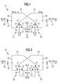
- FIG. 2 shows the principle of so-called “body synchronous sensing" shown where the unwanted Threshold voltage increase is avoided by using source and Body are kept at the same potential.
- the wiring of the N-latch part is one Sense amplifiers in so-called "super body synchronous sensing" shown.
- the Body tension can be adjusted.
- the body voltage is set so that the source body voltage becomes positive and thus via the substrate control influence the threshold voltage of the evaluation transistors is reduced.
- a positive source body voltage means that the source bulk diodes are polarized in the direction of flow.
- the Sensing scheme can therefore only be used for voltage levels apply where the resulting forward current is so small is that it doesn't have a detrimental effect.
- the present invention the object of a Sense amplifier subcircuit for a DRAM memory and to further improve a DRAM memory such that the Evaluation of the memory cells even with small array voltages can be done in an acceptably short time.
- the sense amplifier subcircuit is characterized in that at least one the evaluation transistors is designed such that its threshold voltage during the evaluation process changed dynamically by changing the gate voltage is coupled with a change in bulk voltage.
- the sense amplifier subcircuit according to the invention makes it possible, the DRAM memory cells even at low array voltages to evaluate in an acceptably short time.
- the reinforcing effect of the invention Sense amplifier subcircuit is subsequently based on an N latch part clarifies.
- This effect is based on the one hand that the evaluator transistor with the higher gate voltage a capacitance connected to its drain discharges faster after 0 volts than the evaluation transistor the lower initial gate voltage.
- the faster sinking bit line levels in turn couples to the gate of the anyway poorly conducting transistor and closes it further.
- This reinforcing effect is now according to the invention increases that the threshold voltage of the more conductive Transistor shrinks dynamically while the Threshold voltage of the poorly conducting transistor dynamic enlarged.
- An advantage of the sense amplifier circuit according to the invention compared to the "super body synchronous sensing" known from the prior art is that the invention Sense amplifier subcircuit without additional control lines, for the N and P bodies of the P and N latches. The timing for the control of the bodies (bulks) can thus omitted. Only then will the dynamic change of the Threshold voltage of the at least one evaluation transistor enables because the body tension at the same time and in direct dependence on the gate voltage changes.
- F is the minimal lithographic Structure size understood.
- the dynamic change in the threshold voltage can be advantageous can be realized in that the bulk (or the Body) and the gate of the at least one evaluation transistor are connected via a connection.
- the source-drain diode of the at least one is preferably Pole evaluator transistor polarized in the direction of flow.
- the invention Therefore use the scheme for those voltage levels at which the resulting forward current is so small that it is does not have an adverse effect.
- the invention can be advantageous Sense amplifier subcircuit as a circuit for producing the Low level (N-Latch) and / or as a circuit for manufacturing of the high level (P-latch).
- the at least one evaluation transistor can advantageously be used as SOI transistor can be formed.
- SOI transistors are therefore particularly suitable since you have a separate area needed, which forms the bulk area (body area).
- body area is also possible, however with much more effort and therefore with much higher cost, so the use of SOI transistors is preferred.
- a DRAM memory provided with a number of DRAM memory cells, those via bit lines with at least one Read / write amplifiers are connected, the read / write amplifier also with at least one reference bit line is connected, characterized in that the Read / write amplifier for amplifying from one Bit line read out voltage signals one or more as described above according to the invention Sense amplifier subcircuit (s).
- One as described above is particularly preferred sense amplifier subcircuit according to the invention for evaluation small array voltages of ⁇ 1 volt are used.
- the sense amplifier subcircuit 10 has two Evaluation transistors 20, 30, the Evaluation transistors 20, 30 each have a gate 21, 31, one Source 22, 32, a drain 23, 33 and a bulk 24, 34 feature.
- the evaluation transistors 20, 30 are so-called SOI transistors designed so that the bulk also as a body is referred to and this designation in the further course of Figure description is used.
- the gate 21 of the evaluation transistor 20 is via a Connection 25 (VBLEQ ⁇ ⁇ ) to a bit line (bit line) 50 connected.
- the gate 31 of the evaluation transistor 30 is over a connection (VBLEQ) 35 to a reference bit line (Ref. Bitline) 51 connected.
- the sources 22, 32 of the evaluation transistors 20, 30 are over corresponding connections 27, 37 with a feed line 11 connected, which in the present example is a so-called Is NCS line via which the sense amplifier subcircuit 10, which is designed as an N-latch part is activated.
- the drains 23, 33 of the evaluation transistors 20, 30 are over corresponding connections 26, 36 to the bit lines 50, 51 connected and are in contact with capacities 52, 53.
- the sense amplifier subcircuit 10 is a so-called N-latch
- the The task is to read one from bit line 50 Amplify voltage signal to the low level.
- This low level can be, for example, 0 volts.
- the bit line level is on all bit lines, that is in the exemplary embodiment on the Bit line 50 and the reference bit line 51, approximately half array voltage VBLEQ. Since the DRAM memory cell to be evaluated has an informational content, that is Voltage signal on the bit line to be read by one certain amount ⁇ depending on the information content in the cell either enlarged or reduced.
- Sense amplifier subcircuit 10 is therefore not suitable Evaluations of DRAM memory cells at low array voltages of ⁇ 1 volt in an acceptably short time to be able to.
- the sense amplifier subcircuit 10 shown in FIG undesirable increase in threshold voltage at the Evaluator transistors 20, 30 avoided in that the sources 22, 32 and bodies 24, 34 of the evaluation transistors 20, 30 the same potential. Sources 22, 32 and bodies 24, 34 connected to each other and thus at the same potential regardless of the NCS voltage.
- the wiring is a Sense amplifier subcircuit 10, for example the N latch part of the sense amplifier in the well-known super body synchronous sensing shown.
- the basic structure as well as the Basic operation of the sense amplifier subcircuit 10 correspond in turn to that shown in FIGS. 1 and 2 Embodiments, so that the same components in turn are provided with identical reference numbers and to avoid them from repetitions to the description of FIGS. 1 and 2 is referred.
- Embodiments may include bodies 24, 34 of FIGS Evaluation transistors 20, 30 via a separate line certain potential are laid. At the start of the evaluation the body voltage is set so that the source body voltage becomes positive. About the substrate control influence can thus the threshold voltage of the evaluation transistors 20, 30 be reduced.
- a disadvantage of this embodiment is however, that additional control lines are required to to be able to adjust the body tension. Furthermore must Control circuits are provided, which are the timing for the Controlling the bodies 24, 34 regulate.
- FIG. 4 a modified sense amplifier subcircuit according to the invention 10 as proposed, for example, in FIG. 4 is shown.
- Figure 4 the principle of sense amplifier subcircuit 10 according to the invention using the N-latch part shown.
- the sense amplifier subcircuit 10 can however, also be formed analogously as a P-latch part and act.
- the basic structure corresponds to the Basic operation of the sense amplifier subcircuit 10 in 1 to 3 illustrated embodiments, so that in turn the same components with identical reference numbers are provided.
- the description is in view with reference to Figures 1 to 3.
- the sense amplifier subcircuit 10 is such trained that the threshold voltages of the two Evaluation transistors 20, 30 depending on their gate voltages or change from the bit line levels.
- the gates 21, 31 and bodies 24, 34 of the Evaluation transistors 20, 30 each via a connection 40 connected with each other.
- the amplifying effect of the sense amplifier subcircuit 10 is based on the one hand on the fact that the evaluation transistor 20 with the higher gate voltage (for better understanding again the one with regard to the example according to FIG. 1 conditions mentioned) attached to its drain 23 connected capacity 53 discharges faster after 0 volts than the evaluator transistor 30 with the lower initial Gate voltage.
- the faster falling bit line level couples in turn to the gate 31 of the worse anyway conductive transistor 30 and closes it further.
- the reinforcing effect is now increased by the fact that the threshold voltage of the more conductive transistor 20 because the connection 40 between the body 24 and the gate 21 dynamically reduced while the operating voltage of the poorly conductive transistor 30 dynamically enlarged.
- the change in the gate voltage is via the connection 40 coupled with the change in body tension so that the better conducting evaluator transistor 20 much faster still becomes more conductive, while the less conductive anyway Evaluator transistor 30 much worse even worse becomes a leader.
Landscapes
- Engineering & Computer Science (AREA)
- Microelectronics & Electronic Packaging (AREA)
- Computer Hardware Design (AREA)
- Dram (AREA)
Abstract
Description
Claims (8)
- Leseverstärkerteilschaltung für einen DRAM-Speicher zum Verstärken von aus einer Bitleitung (50) ausgelesenen Spannungssignalen, mit wenigstens zwei Bewertertransistoren (20; 30), wobei das Gate (21) eines Bewertertransistors (20) mit wenigstens einer Bitleitung (50) und das Gate (31) eines anderen Bewertertransistors (30) mit wenigstens einer Referenz-Bitleitung (51) verbunden oder verbindbar ist und wobei die Drains (23, 33) der Bewertertransistoren (20; 30) mit den bitleitungen (51, 50) und die Sources (22, 32) der Bewertertransistoren (20; 30) mit einer Zuleitung (11) verbunden oder verbindbar sind,
dadurch gekennzeichnet, daß zumindest einer der Bewertertransistoren (20; 30) derart ausgebildet ist, daß sich dessen Einsatzspannung während des Bewertungsvorgangs dynamisch verändert, indem die Veränderung der Gate-Spannung mit einer Veränderung der Bulk-Spannung gekoppelt ist. - Leseverstärkerteilschaltung nach Anspruch 1,
dadurch gekennzeichnet, daß der Bulk ( 24; 34) und das Gate (21, 31) des zumindest einen Bewertertransistors (20; 30) über eine Verbindung (40) miteinander verbunden sind. - Leseverstärkerteilschaltung nach Anspruch oder 2,
dadurch gekennzeichnet, daß die Source-Drain-Diode des zumindest einen Bewertertransistors (20; 30) in Flußrichtung gepolt ist. - Leseverstärkerteilschaltung nach einem der Ansprüche 1 bis
3, dadurch gekennzeichnet, daß diese als Schaltung zur Herstellung des Low-Pegels (N-Latch) ausgebildet ist. - Leseverstärkerteilschaltung nach einem der Ansprüche 1 bis
3, dadurch gekennzeichnet, daß diese als Schaltung zur Herstellung des High-Pegels (P-Latch) ausgebildet ist. - Leseverstärkerteilschaltung nach einem der Ansprüche 1 bis
5, dadurch gekennzeichnet, daß der wenigstens eine Bewertertransistor (20; 30) als SOI-Transistor ausgebildet ist. - DRAM-Speicher mit einer Anzahl von DRAM-Speicherzellen, die über Bitleitungen mit wenigstens einem Schreib-Leseverstärker verbunden sind, wobei der Schreib-Leseverstärker ebenfalls mit wenigstens einer Referenz-Bitleitung verbunden ist,
dadurch gekennzeichnet, daß der Schreib-Leseverstärker zur Verstärkung von aus einer Bitleitung ausgelesenen Spannungssignalen eine oder mehrere Leseverstärkerteilschaltung(en) (10) nach einem der Ansprüche 1 bis 6 aufweist. - Verwendung einer Leseverstärkerteilschaltung nach einem der Ansprüche 1 bis 6 zum Bewerten kleiner Array-Spannungen von ≤ 1 Volt.
Applications Claiming Priority (2)
| Application Number | Priority Date | Filing Date | Title |
|---|---|---|---|
| DE10010886 | 2000-03-06 | ||
| DE10010886A DE10010886C1 (de) | 2000-03-06 | 2000-03-06 | Leseverstärkerteilschaltung für einen DRAM-Speicher und entsprechender DRAM-Speicher |
Publications (1)
| Publication Number | Publication Date |
|---|---|
| EP1134745A1 true EP1134745A1 (de) | 2001-09-19 |
Family
ID=7633704
Family Applications (1)
| Application Number | Title | Priority Date | Filing Date |
|---|---|---|---|
| EP01104593A Withdrawn EP1134745A1 (de) | 2000-03-06 | 2001-03-06 | Leseverstärkerteilschaltung für einen DRAM-Speicher |
Country Status (4)
| Country | Link |
|---|---|
| US (1) | US6452850B1 (de) |
| EP (1) | EP1134745A1 (de) |
| DE (1) | DE10010886C1 (de) |
| TW (1) | TW540052B (de) |
Family Cites Families (3)
| Publication number | Priority date | Publication date | Assignee | Title |
|---|---|---|---|---|
| JP3549602B2 (ja) * | 1995-01-12 | 2004-08-04 | 株式会社ルネサステクノロジ | 半導体記憶装置 |
| DE69632098T2 (de) * | 1995-04-21 | 2005-03-24 | Nippon Telegraph And Telephone Corp. | MOSFET Schaltung und ihre Anwendung in einer CMOS Logikschaltung |
| JP3589557B2 (ja) * | 1997-12-24 | 2004-11-17 | シャープ株式会社 | センスアンプ回路 |
-
2000
- 2000-03-06 DE DE10010886A patent/DE10010886C1/de not_active Expired - Fee Related
-
2001
- 2001-03-06 EP EP01104593A patent/EP1134745A1/de not_active Withdrawn
- 2001-03-06 US US09/799,940 patent/US6452850B1/en not_active Expired - Lifetime
- 2001-04-10 TW TW090105011A patent/TW540052B/zh not_active IP Right Cessation
Non-Patent Citations (1)
| Title |
|---|
| KUGE S ET AL: "SOI-DRAM CIRCUIT TECHNOLOGIES FOR LOW POWER HIGH SPEED MULTIGIGA SCALE MEMORIES", IEEE JOURNAL OF SOLID-STATE CIRCUITS,IEEE INC. NEW YORK,US, vol. 31, no. 4, 1 April 1996 (1996-04-01), pages 586 - 591, XP000597231, ISSN: 0018-9200 * |
Also Published As
| Publication number | Publication date |
|---|---|
| US6452850B1 (en) | 2002-09-17 |
| TW540052B (en) | 2003-07-01 |
| DE10010886C1 (de) | 2002-01-17 |
| US20020024854A1 (en) | 2002-02-28 |
Similar Documents
| Publication | Publication Date | Title |
|---|---|---|
| DE4035660C2 (de) | Elektrisch programmierbare Speichereinrichtung und Verfahren zum Zugreifen/Programmieren von Speicherzellen | |
| DE69422915T2 (de) | Leseverstärker-organisation | |
| DE69027065T2 (de) | Halbleiterspeicheranordnung | |
| DE69322237T2 (de) | Leseverstärker für einen integrierten Speicher | |
| DE2919166C2 (de) | Speichervorrichtung | |
| DE69621165T2 (de) | Ferroelektrischer Speicher und Verfahren für seine Betriebswirkung | |
| DE10255102B3 (de) | SRAM-Speicherzelle mit Mitteln zur Erzielung eines vom Speicherzustand unabhängigen Leckstroms | |
| DE102014117963A1 (de) | Wortleitungsaktivierung | |
| DE3236729C2 (de) | ||
| DE4226844C2 (de) | Datenübertragungsschaltkreis | |
| DE60003451T2 (de) | Wortleitungssignale einer flashspeicher bleiben überall auf dem chip verlustfrei | |
| DE4138102C2 (de) | Halbleiterspeichereinrichtung und Verfahren zum Betreiben einer Halbleiterspeichereinrichtung | |
| DE60020624T2 (de) | Ferroelektrischer Speicher | |
| EP1153394B1 (de) | Verfahren zum betrieb einer speicherzellenanordnung mit selbstverstärkenden dynamischen speicherzellen | |
| DE3780492T2 (de) | Halbleiterspeicheranordnung. | |
| DE102006022867A1 (de) | Ausleseschaltung für oder in einem ROM-Speicher, ROM-Speicher und Verfahren zum Auslesen des ROM-Speichers | |
| DE19621769C1 (de) | Leseverstärker für Halbleiterspeicherzellen mit einer Einrichtung zur Kompensation von Schwellenspannungsunterschieden bei den Leseverstärkertransistoren | |
| DE10107314C2 (de) | Verfahren zum Lesen einer Speicherzelle eines Halbleiterspeichers und Halbleiterspeicher | |
| DE2935121C2 (de) | ||
| EP1134745A1 (de) | Leseverstärkerteilschaltung für einen DRAM-Speicher | |
| EP1148509A1 (de) | Leseverstärker | |
| DE10038383C1 (de) | Hochgeschwindigkeits-Lese-Stromverstärker | |
| DE10322544B3 (de) | DRAM-Speicherschaltung | |
| EP1094465A1 (de) | Speichereinrichtung | |
| DE3938638A1 (de) | Halbleiterspeichereinrichtung mit einem verbesserten leseverstaerker vom stromtyp mit hoher betriebsgeschwindigkeit und verfahren zu dessen betreibung |
Legal Events
| Date | Code | Title | Description |
|---|---|---|---|
| PUAI | Public reference made under article 153(3) epc to a published international application that has entered the european phase |
Free format text: ORIGINAL CODE: 0009012 |
|
| AK | Designated contracting states |
Kind code of ref document: A1 Designated state(s): AT BE CH CY DE DK ES FI FR GB GR IE IT LI LU MC NL PT SE TR Kind code of ref document: A1 Designated state(s): DE FR |
|
| AX | Request for extension of the european patent |
Free format text: AL;LT;LV;MK;RO;SI |
|
| 17P | Request for examination filed |
Effective date: 20020314 |
|
| AKX | Designation fees paid |
Free format text: DE FR |
|
| 17Q | First examination report despatched |
Effective date: 20071106 |
|
| GRAP | Despatch of communication of intention to grant a patent |
Free format text: ORIGINAL CODE: EPIDOSNIGR1 |
|
| STAA | Information on the status of an ep patent application or granted ep patent |
Free format text: STATUS: THE APPLICATION IS DEEMED TO BE WITHDRAWN |
|
| 18D | Application deemed to be withdrawn |
Effective date: 20091020 |