EP1134721A2 - Display apparatus comprising two display regions and portable electronic apparatus that can reduce power consumption, and method of driving the same - Google Patents
Display apparatus comprising two display regions and portable electronic apparatus that can reduce power consumption, and method of driving the same Download PDFInfo
- Publication number
- EP1134721A2 EP1134721A2 EP01250055A EP01250055A EP1134721A2 EP 1134721 A2 EP1134721 A2 EP 1134721A2 EP 01250055 A EP01250055 A EP 01250055A EP 01250055 A EP01250055 A EP 01250055A EP 1134721 A2 EP1134721 A2 EP 1134721A2
- Authority
- EP
- European Patent Office
- Prior art keywords
- vgn
- scanning
- display
- scanning lines
- inputted
- Prior art date
- Legal status (The legal status is an assumption and is not a legal conclusion. Google has not performed a legal analysis and makes no representation as to the accuracy of the status listed.)
- Granted
Links
Images





Classifications
-
- G—PHYSICS
- G09—EDUCATION; CRYPTOGRAPHY; DISPLAY; ADVERTISING; SEALS
- G09G—ARRANGEMENTS OR CIRCUITS FOR CONTROL OF INDICATING DEVICES USING STATIC MEANS TO PRESENT VARIABLE INFORMATION
- G09G3/00—Control arrangements or circuits, of interest only in connection with visual indicators other than cathode-ray tubes
- G09G3/20—Control arrangements or circuits, of interest only in connection with visual indicators other than cathode-ray tubes for presentation of an assembly of a number of characters, e.g. a page, by composing the assembly by combination of individual elements arranged in a matrix no fixed position being assigned to or needed to be assigned to the individual characters or partial characters
-
- G—PHYSICS
- G09—EDUCATION; CRYPTOGRAPHY; DISPLAY; ADVERTISING; SEALS
- G09G—ARRANGEMENTS OR CIRCUITS FOR CONTROL OF INDICATING DEVICES USING STATIC MEANS TO PRESENT VARIABLE INFORMATION
- G09G3/00—Control arrangements or circuits, of interest only in connection with visual indicators other than cathode-ray tubes
- G09G3/20—Control arrangements or circuits, of interest only in connection with visual indicators other than cathode-ray tubes for presentation of an assembly of a number of characters, e.g. a page, by composing the assembly by combination of individual elements arranged in a matrix no fixed position being assigned to or needed to be assigned to the individual characters or partial characters
- G09G3/34—Control arrangements or circuits, of interest only in connection with visual indicators other than cathode-ray tubes for presentation of an assembly of a number of characters, e.g. a page, by composing the assembly by combination of individual elements arranged in a matrix no fixed position being assigned to or needed to be assigned to the individual characters or partial characters by control of light from an independent source
- G09G3/36—Control arrangements or circuits, of interest only in connection with visual indicators other than cathode-ray tubes for presentation of an assembly of a number of characters, e.g. a page, by composing the assembly by combination of individual elements arranged in a matrix no fixed position being assigned to or needed to be assigned to the individual characters or partial characters by control of light from an independent source using liquid crystals
- G09G3/3611—Control of matrices with row and column drivers
- G09G3/3674—Details of drivers for scan electrodes
- G09G3/3677—Details of drivers for scan electrodes suitable for active matrices only
-
- G—PHYSICS
- G09—EDUCATION; CRYPTOGRAPHY; DISPLAY; ADVERTISING; SEALS
- G09G—ARRANGEMENTS OR CIRCUITS FOR CONTROL OF INDICATING DEVICES USING STATIC MEANS TO PRESENT VARIABLE INFORMATION
- G09G3/00—Control arrangements or circuits, of interest only in connection with visual indicators other than cathode-ray tubes
- G09G3/20—Control arrangements or circuits, of interest only in connection with visual indicators other than cathode-ray tubes for presentation of an assembly of a number of characters, e.g. a page, by composing the assembly by combination of individual elements arranged in a matrix no fixed position being assigned to or needed to be assigned to the individual characters or partial characters
- G09G3/34—Control arrangements or circuits, of interest only in connection with visual indicators other than cathode-ray tubes for presentation of an assembly of a number of characters, e.g. a page, by composing the assembly by combination of individual elements arranged in a matrix no fixed position being assigned to or needed to be assigned to the individual characters or partial characters by control of light from an independent source
- G09G3/36—Control arrangements or circuits, of interest only in connection with visual indicators other than cathode-ray tubes for presentation of an assembly of a number of characters, e.g. a page, by composing the assembly by combination of individual elements arranged in a matrix no fixed position being assigned to or needed to be assigned to the individual characters or partial characters by control of light from an independent source using liquid crystals
-
- G—PHYSICS
- G09—EDUCATION; CRYPTOGRAPHY; DISPLAY; ADVERTISING; SEALS
- G09G—ARRANGEMENTS OR CIRCUITS FOR CONTROL OF INDICATING DEVICES USING STATIC MEANS TO PRESENT VARIABLE INFORMATION
- G09G3/00—Control arrangements or circuits, of interest only in connection with visual indicators other than cathode-ray tubes
- G09G3/20—Control arrangements or circuits, of interest only in connection with visual indicators other than cathode-ray tubes for presentation of an assembly of a number of characters, e.g. a page, by composing the assembly by combination of individual elements arranged in a matrix no fixed position being assigned to or needed to be assigned to the individual characters or partial characters
- G09G3/34—Control arrangements or circuits, of interest only in connection with visual indicators other than cathode-ray tubes for presentation of an assembly of a number of characters, e.g. a page, by composing the assembly by combination of individual elements arranged in a matrix no fixed position being assigned to or needed to be assigned to the individual characters or partial characters by control of light from an independent source
- G09G3/36—Control arrangements or circuits, of interest only in connection with visual indicators other than cathode-ray tubes for presentation of an assembly of a number of characters, e.g. a page, by composing the assembly by combination of individual elements arranged in a matrix no fixed position being assigned to or needed to be assigned to the individual characters or partial characters by control of light from an independent source using liquid crystals
- G09G3/3611—Control of matrices with row and column drivers
- G09G3/3648—Control of matrices with row and column drivers using an active matrix
-
- G—PHYSICS
- G09—EDUCATION; CRYPTOGRAPHY; DISPLAY; ADVERTISING; SEALS
- G09G—ARRANGEMENTS OR CIRCUITS FOR CONTROL OF INDICATING DEVICES USING STATIC MEANS TO PRESENT VARIABLE INFORMATION
- G09G3/00—Control arrangements or circuits, of interest only in connection with visual indicators other than cathode-ray tubes
- G09G3/20—Control arrangements or circuits, of interest only in connection with visual indicators other than cathode-ray tubes for presentation of an assembly of a number of characters, e.g. a page, by composing the assembly by combination of individual elements arranged in a matrix no fixed position being assigned to or needed to be assigned to the individual characters or partial characters
- G09G3/34—Control arrangements or circuits, of interest only in connection with visual indicators other than cathode-ray tubes for presentation of an assembly of a number of characters, e.g. a page, by composing the assembly by combination of individual elements arranged in a matrix no fixed position being assigned to or needed to be assigned to the individual characters or partial characters by control of light from an independent source
- G09G3/36—Control arrangements or circuits, of interest only in connection with visual indicators other than cathode-ray tubes for presentation of an assembly of a number of characters, e.g. a page, by composing the assembly by combination of individual elements arranged in a matrix no fixed position being assigned to or needed to be assigned to the individual characters or partial characters by control of light from an independent source using liquid crystals
- G09G3/3611—Control of matrices with row and column drivers
- G09G3/3648—Control of matrices with row and column drivers using an active matrix
- G09G3/3666—Control of matrices with row and column drivers using an active matrix with the matrix divided into sections
-
- G—PHYSICS
- G09—EDUCATION; CRYPTOGRAPHY; DISPLAY; ADVERTISING; SEALS
- G09G—ARRANGEMENTS OR CIRCUITS FOR CONTROL OF INDICATING DEVICES USING STATIC MEANS TO PRESENT VARIABLE INFORMATION
- G09G2310/00—Command of the display device
- G09G2310/06—Details of flat display driving waveforms
- G09G2310/065—Waveforms comprising zero voltage phase or pause
-
- G—PHYSICS
- G09—EDUCATION; CRYPTOGRAPHY; DISPLAY; ADVERTISING; SEALS
- G09G—ARRANGEMENTS OR CIRCUITS FOR CONTROL OF INDICATING DEVICES USING STATIC MEANS TO PRESENT VARIABLE INFORMATION
- G09G2330/00—Aspects of power supply; Aspects of display protection and defect management
- G09G2330/02—Details of power systems and of start or stop of display operation
- G09G2330/021—Power management, e.g. power saving
-
- G—PHYSICS
- G09—EDUCATION; CRYPTOGRAPHY; DISPLAY; ADVERTISING; SEALS
- G09G—ARRANGEMENTS OR CIRCUITS FOR CONTROL OF INDICATING DEVICES USING STATIC MEANS TO PRESENT VARIABLE INFORMATION
- G09G2330/00—Aspects of power supply; Aspects of display protection and defect management
- G09G2330/02—Details of power systems and of start or stop of display operation
- G09G2330/021—Power management, e.g. power saving
- G09G2330/022—Power management, e.g. power saving in absence of operation, e.g. no data being entered during a predetermined time
-
- G—PHYSICS
- G09—EDUCATION; CRYPTOGRAPHY; DISPLAY; ADVERTISING; SEALS
- G09G—ARRANGEMENTS OR CIRCUITS FOR CONTROL OF INDICATING DEVICES USING STATIC MEANS TO PRESENT VARIABLE INFORMATION
- G09G3/00—Control arrangements or circuits, of interest only in connection with visual indicators other than cathode-ray tubes
- G09G3/20—Control arrangements or circuits, of interest only in connection with visual indicators other than cathode-ray tubes for presentation of an assembly of a number of characters, e.g. a page, by composing the assembly by combination of individual elements arranged in a matrix no fixed position being assigned to or needed to be assigned to the individual characters or partial characters
- G09G3/34—Control arrangements or circuits, of interest only in connection with visual indicators other than cathode-ray tubes for presentation of an assembly of a number of characters, e.g. a page, by composing the assembly by combination of individual elements arranged in a matrix no fixed position being assigned to or needed to be assigned to the individual characters or partial characters by control of light from an independent source
- G09G3/36—Control arrangements or circuits, of interest only in connection with visual indicators other than cathode-ray tubes for presentation of an assembly of a number of characters, e.g. a page, by composing the assembly by combination of individual elements arranged in a matrix no fixed position being assigned to or needed to be assigned to the individual characters or partial characters by control of light from an independent source using liquid crystals
- G09G3/3611—Control of matrices with row and column drivers
- G09G3/3614—Control of polarity reversal in general
Definitions
- the present invention relates to a display apparatus and a method of driving a display apparatus. More particularly, the present invention relates to a liquid crystal display and a method of driving a liquid crystal display.
- JP-A-Heisei, 6-95621 discloses the following liquid crystal display controller.
- the liquid crystal display controller for controlling a display apparatus of a liquid crystal panel has a driver for dividing a display region of the liquid crystal panel into a plurality of partial display regions, and making a partial display region selected by an external control signal at a drive state and making the other partial display regions at a non-drive state.
- JP-A-Heisei, 7-281632 discloses the following liquid crystal display.
- This has a common electrode in using an entire region of a liquid crystal display panel targeted for a display apparatus, a common electrode in using a partial region of the liquid crystal display panel having an effective peak value smaller than a drive voltage to a segment electrode, and a power supply circuit for switching and outputting the drive voltage to the segment electrode through an operation of a switch. It drives by switching between the segment electrode and the common electrode corresponding to the partial region or the entire region of the liquid crystal display panel, in accordance with the drive voltage from the power supply circuit.
- Another object of the present invention is to provide a display apparatus of an active matrix drive type represented by a TFT method that can reduce consumptive power.
- the first intervals may be selected such that the plurality of capacitance sections of the first display region are driven at alternating currents
- the second intervals may be selected such that the plurality of capacitance sections of the second display region are driven at alternating currents.
- the plurality of display signals inputted to the plurality of capacitance sections of the second display region may have amplitudes substantially identical with each other.
- a plurality of specific display signals having amplitudes substantially identical with the amplitudes of the plurality of display signals inputted to the plurality of capacitance sections of the second display region when the plurality of scanning signals are inputted to the second group of the scanning lines, are outputted to the plurality of signal lines at the same timings as when the plurality of scanning signals are inputted to the second group of the scanning lines.
- potentials of the second group of the scanning lines may be dropped at the same timings as when the plurality of scanning signals are inputted to the second group of the scanning lines.
- a shift register supplying the plurality of scanning lines to the plurality of scanning signals by transferring an input signal one by one, and wherein the shift register has a switch to stop transferring the input signal such that the plurality of scanning signals are supplied to the first group of the scanning lines and the plurality of scanning signals are not supplied to the second group of the scanning lines.
- the input signal may be transferred in a predetermined direction in the shift register, and wherein a first input section inputting the input signal is provided in the most upstream in the predetermined direction of the first group of the scanning lines in the shift resister, and wherein a second input section inputting the input signal is provided in the most upstream in the predetermined direction of the second group of the scanning lines in the shift resister.
- a display apparatus includes: a plurality of scanning lines to which a plurality of scanning signals are inputted, respectively; a plurality of signal lines to which a plurality of display signals are inputted, respectively; a plurality of capacitance sections respectively provided through a plurality of switching elements at a plurality of intersections of the plurality of scanning lines and the plurality of signal lines; and a display section including the plurality of capacitance sections, and wherein the display section is divided into first, second and third display regions by two virtual lines parallel to at least one of the plurality of scanning lines, and wherein the plurality of scanning signals are inputted at first intervals to a first group of the scanning lines corresponding to the first display region of the plurality of scanning lines, and wherein the plurality of scanning signals are inputted at second intervals to a second group of the scanning lines corresponding to the second display region of the plurality of scanning lines, and wherein the plurality of scanning signals are inputted at third intervals to a third group of the scanning
- a portable electronic apparatus has a display apparatus which includes: a plurality of scanning lines to which a plurality of scanning signals are inputted, respectively; a plurality of signal lines to which a plurality of display signals are inputted, respectively; a plurality of capacitance sections respectively provided through a plurality of switching elements at a plurality of intersections of the plurality of scanning lines and the plurality of signal lines; and a display section including the plurality of capacitance sections, and wherein the display section is divided into first and second display regions by a virtual line parallel to at least one of the plurality of scanning lines, and wherein the plurality of scanning signals are inputted at first intervals to a first group of the scanning lines corresponding to the first display region of the plurality of scanning lines, and wherein the plurality of scanning signals are inputted at second intervals different from the first intervals to a second group of the scanning lines corresponding to the second display region of the plurality of scanning lines.
- the first intervals may be selected such that the plurality of capacitance sections of the first display region are driven at alternating currents
- the second intervals are selected such that the plurality of capacitance sections of the second display region are driven at alternating currents.
- the display apparatus of the present invention is based on the active matrix drive method, and has a plurality of regions having different refresh rates (a display rate, a write frequency and an gate-on period) on a single screen.
- the active method is used to control the voltages applied to a scanning line of a second display region, a signal line, an opposite common electrode and a liquid crystal.
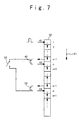
- the display signal is written to the capacity 22 of each pixel (the capacity 22 includes both a liquid crystal capacity and an accumulation capacity) through a TFT switch 20 that is controlled to be turned on and off, in accordance with the scanning signal.
- a liquid crystal on each pixel electrode is operated on the basis of a potential difference between a pixel electrode voltage VD corresponding to the display signal and the opposite common voltage VCOM at that time.
- the operation for writing the display signal to the pixel electrode (capacity 22) is carried out by using a method of sampling a parallel display signal to be simultaneously sent to the signal lines S1, S2 ⁇ by using a scanning signal to be sequentially sent to the plurality of scanning lines G1, G2, ⁇ Gn, Gn+1 ⁇ (Line Sequence Drive).
- an LCD panel 30 is divided into an upper half (first display region) 31 and a lower half (second display region) 32, and it is driven.
- the first display region 31 is in a range between the scanning lines G1, G2, ⁇ , Gn-1.
- the second display region 32 is in a range between the scanning lines Gn, Gn+1 ⁇ .
- the time band in which the picture of the second display region 32 is not changed in picture, does not require that the scanning signal is sent to the scanning lines Gn, Gn+1 ⁇ of the second display region 32.
- a display signal when a scanning signal is sent to the scanning lines Gn, Gn+1 ⁇ immediately before the time band is held in a capacity section 22 of the second display region 32.
- the voltage of the display signal when the scanning signal is sent to the scanning lines Gn, Gn+1 ⁇ is equal to or less than a threshold and immediately after its supply, the scanning signal is not sent to the scanning lines Gn, Gn+1 ⁇ , the screen of the second display region 32 is kept white when a liquid crystal of each pixel is a normally white type.
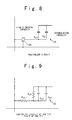
- a TFT type LCD has a parasitic resistance, and a leak current is induced from a pixel potential.
- the pixel potential is not always attenuated in a direction of a zero volt, in both the positive write and the negative write such as a field through voltage and the like. It may occur that an unexpected direct current voltage is applied to the liquid crystal, and this case leads to a factor of a deterioration. For this reason, even in the second display region 32 in which the consumptive power is reduced, it is not desirable to stop the supply of the scanning signal for a long time. It is necessary that the scanning signal is sent even if the write period is long.
- ⁇ RLC ⁇ (CLC + CST).
- the off resistance RTFT of the TFT 20 does not exhibit a merely linear resistive property because of a fluctuation of a process for manufacturing the TFT 20 and exhibits a non-linear property in which the property is changed depending on a voltage and a polarity. Thus, it is impossible to expect the simply discharging/charging property.
- the continuation of the off-state of the TFT 20 causes the voltages written to the liquid crystal capacity CLC and the accumulation capacity CST to be gradually changed.
- the direction of the change is not uniform.
- the continuation of this changed state causes the direct current voltage to be continuously applied to the liquid crystal.
- fear may occur that the molecules of the liquid crystal within the liquid crystal panel and the related material are dissolved to thereby bring about the aging deterioration.
- both the resistor value RLC of the liquid crystal capacity and the off resistance RTFT of the TFT 20 are sufficiently large. Thus, there is no problem with regard to the discharging/charging action.
- this embodiment uses the feature of the hold device for holding the voltage at which the TFT type LCD is written, and makes the write period longer and drives it, and accordingly attains both the maintenance of the original reliability and the reduction in the consumptive power.
- the fact that the liquid crystal driven at the long write period needs to be driven at the alternating current is similar to that of the liquid crystal driven at the usual write period.
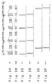
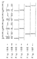
- Figs. 3A ⁇ 3F show a case in which a picture of the second display region 32 is not changed in picture (including a case that the entire surface of the second display region 32 is still kept white).
- a picture corresponding to a lengthened write period (this picture has the picture change smaller than that of the picture of the first display region 31 of the usual write period) is displayed on the second display region 32.
- a scanning signal VGn is sent to the scanning line Gn of the second display region 32 at the usual timing (the timing equal to that of Fig. 2).
- a scanning signal VGn+1 is sent to the scanning line Gn+1 of the second display region 32 at the usual timing (the timing equal to that of Fig. 2). That is, in the first frame FT, the scanning signals are sequentially inputted to all the scanning lines G1, G2, ⁇ Gn, Gn+1 ⁇ of the LCD panel 30. Thus, not only the first display region 31 but also the second display region 32 is driven.
- voltage VS of the display signal sent to the liquid crystal capacity 22 connected through the TFT 20 to the scanning line Gn+2 when the scanning signal VGn+2 is sent to the scanning line Gn+2 and voltage VS of the display signal sent to the liquid crystal capacity 22 connected through the TFT 20 to the scanning line Gn+1 when the scanning signal VGn+1 is sent to the scanning line Gn+1 are different from each other in polarity and equal to each other in amplitude.
- the values of the voltages applied to the respective capacities 22 are equal to each other (the absolute value of the potential difference between the VD and the VCOM). They are equal to or less than the threshold of the liquid crystal of each pixel. Thus, each pixel becomes white in the same graduation.
- the above-mentioned display signal VS shown in Fig. 3A corresponds to any one of the plurality of signal lines S1, S2 ⁇ (here, it is assumed to be the signal line S1).
- the other signal lines here, they are assumed to be the signal lines S2, S3 ⁇
- the scanning signals VGn, VGn+1 ⁇ are sent to the scanning lines Gn, Gn+1 ⁇
- the value of the display signal sent to each of the liquid crystal capacities 22 connected through the TFTs 20 to the scanning lines Gn, Gn+1 ⁇ is equal to any one of the above-mentioned signal lines (signal line S1).
- the whole of the second display region 32 is white in the same gradation.
- the second frame FT will be described below.
- the scanning signal VG1, VG2, ⁇ VGn-1 ⁇ are sent to the scanning lines G1, G2, ⁇ Gn-1 of the first display region 31, similarly to Figs. 2C and 2D.
- the pulses for turning the TFTs on such as the scanning signals VGn, VGn+1 ⁇ , are not sent to the scanning lines Gn, Gn+1 ⁇ of the second display region 32, differently from Figs. 2E and 2F.
- all the TFTs 20 of the second display region 32 are at the off-state (the second display region 32 is not driven).
- a new voltage (the potential difference between the VD and the VCOM) is never applied to each of the liquid crystal capacities 22 of the second display region 32.
- the voltage applied in the first frame FT is held in each of the liquid crystal capacities 22 of the second display region 32.
- the respective pixels of the second display region 32 are white in the same graduation.
- the charges accumulated in the respective liquid crystal capacities 22 of the second display region 32 may be slightly discharged with an elapse of a time, as compared with the first frame FT. However, if the discharge amount is equal to or less than the threshold voltage of the liquid crystal, no problem on the actual usage occurs.
- the third frame FT will be described below.
- the second display region 32 is not driven similarly to the second frame FT.
- the operation with regard to the second display region 32 is equal to that of the second frame FT.
- the condition of the second display region 32 is equal to that of the second frame FT.
- the charges accumulated in the respective liquid crystal capacities 22 of the second display region 32 may be slightly discharged with an elapse of a time, as compared with the second frame FT. However, if the discharge amount is equal to or less than the threshold voltage of the liquid crystal, no problem on the actual usage occurs.
- the fourth frame FT will be described below.
- the second display region 32 is driven similarly to the first frame FT.
- the operation with regard to the second display region 32 is equal to that of the first frame FT except the following points.
- the voltage VS of the display signal sent to the liquid crystal capacity 22 connected through the TFT 20 to the scanning line Gn when the scanning signal VGn is sent to the scanning line Gn is the positive potential (with the opposite common voltage VCOM as the standard).
- the voltage VS of the display signal sent to the liquid crystal capacity 22 connected through the TFT 20 to the scanning line Gn+1 when the scanning signal VGn+1 is sent to the scanning line Gn+1 is the negative potential (with the opposite common voltage VCOM as the standard).
- each voltage VS of the fourth frame FT is opposite to that of the first frame FT. That is, in the fourth frame FT, the voltage VS of the display signal sent to the liquid crystal capacity 22 connected through the TFT 20 to the scanning line Gn when the scanning signal VGn is sent to the scanning line Gn is the negative potential (with the opposite common voltage VCOM as the standard). The voltage VS of the display signal sent to the liquid crystal capacity 22 connected through the TFT 20 to the scanning line Gn+1 when the scanning signal VGn+1 is sent to the scanning line Gn+1 is the positive potential (with the opposite common voltage VCOM as the standard).
- the liquid crystal of each pixel in the second display region 32 is driven at the alternating current between the first frame FT and the fourth frame FT.
- the voltage VS of the display signal sent to the liquid crystal capacity 22 connected through the TFT 20 to the scanning line Gn when the scanning signal VGn is sent to the scanning line Gn and the voltage VS of the display signal sent to the liquid crystal capacity 22 connected through the TFT 20 to the scanning line Gn+1 when the scanning signal VGn+1 is sent to the scanning line Gn+1 are different from each other in polarity and equal to each other in amplitude, similarly to the first frame FT.
- the values of the voltages applied to the respective capacities 22 are equal to each other (the absolute value of the potential difference between the VD and the VCOM). Each of the values is equal to or less than the threshold of the liquid crystal of each pixel.
- the above-mentioned explanation is described with regard to the scanning lines Gn, Gn+1. The operation in the above-mentioned explanation is repeated for the scanning lines Gn+2, Gn+3, ⁇ .
- the respective liquid crystal capacities 22 of the second display region 32 are only different from each other in polarity. So, they are driven similarly to the first frame FT.
- Each pixel of the second display region 32 is white in the same graduation as the first frame FT.
- the fifth frame FT (not shown) will be described below.
- the operation with regard to the second display region 32 in the fifth frame FT is equal to that of the second frame FT.
- the liquid crystal voltage VLC of each pixel corresponding to each liquid crystal capacity 22 of the second display region 32 in the fifth frame FT is assumed to be equal to the liquid crystal voltage VLC of each pixel corresponding to each liquid crystal capacity 22 of the second display region 32 in the fourth frame FT (fixed from the fourth frame FT).
- the operation with regard to a second display region 32 in a sixth frame FT is equal to that of the third frame FT.
- the operation with regard to a second display region 32 in a seventh frame FT (not shown) is equal to that of the first frame FT.
- the operations on and after an eighth frame FT (not shown) are also similar to those of the above-mentioned frames FT.
- the second display region 32 is driven in the fourth frame FT after the first frame FT. This is because the liquid crystal of each pixel of the second display region 32 is driven at the alternating current between the first frame FT and the fourth frame FT.
- the frame FT in which the second display region 32 is driven can be replaced by the above-mentioned frame FT.
- the second display region 32 can be driven in the fourth frame FT and the sixth frame FT after the first frame FT and the third frame FT.
- the voltage VS of the display signal sent to the liquid crystal capacity 22 connected through the TFT 20 to the scanning line Gn when the scanning signal VGn is sent to the scanning line Gn is the positive potential (with the opposite common voltage VCOM as the standard).
- the voltage VS of the display signal sent to the liquid crystal capacity 22 connected through the TFT 20 to the scanning line Gn+1 when the scanning signal VGn+1 is sent to the scanning line Gn+1 is the negative potential (with the opposite common voltage VCOM as the standard).
- the polarities of the respective voltages VS of the fourth and sixth frames FT are opposite to those of the first and third frames FT. That is, in the fourth frame FT, the voltage VS of the display signal sent to the liquid crystal capacity 22 connected through the TFT 20 to the scanning line Gn when the scanning signal VGn is sent to the scanning line Gn is the negative potential (with the opposite common voltage VCOM as the standard).
- the voltage VS of the display signal sent to the liquid crystal capacity 22 connected through the TFT 20 to the scanning line Gn+1 when the scanning signal VGn+1 is sent to the scanning line Gn+1 is the positive potential (with the opposite common voltage VCOM as the standard).
- the voltages VS of the display signals applied to the respective signal lines S1, S2 ⁇ at the time of the drive of the second display region 32 may be the voltages of the original picture (display) signals which are not always equal to each other in amplitude.
- the signal voltages VS sent to the TFTs 20 connected to the scan electrodes on and after the scan electrode Gn are set to be equal (fixed) to those when the second display region 32 is driven (for example, the first frame FT).
- the potentials of the signal lines S1, S2 ⁇ can be removed or set at a floating state (a high impedance state) at a timing when they are sent to the second display region 32. That is, it is possible to transiently stop the supply of a power supply to a driver IC for driving the signal lines S1, S2 ⁇ or mount an on/off switching switch at former stages of the signal lines S1, S2 ⁇ .
- the scanning lines Gn, Gn+1 ⁇ at the time of the drive of the second display region 32 are scanned by using the line sequence scan manner.
- the number of interlaced scanning lines may be plural.
- the potentials corresponding to the scanning lines Gn, Gn+1 ⁇ may be removed.
- the consumptive power can be further reduced when the voltage VS of the display signal is not changed if possible.
- the liquid crystal of each pixel of the second display region 32 is the normally white type, and the voltage equal to or less than the threshold is applied to each pixel, and it is made white, the amplitude can be made further lower than that of the example of Fig. 3A, as shown in Fig. 10A.
- the consumptive power can be further reduced by setting the amplitude of the voltage VS of the display signal at zero, in the second display region 32.
- the further reduction in the consumptive power can be attained by setting the amplitude of the opposite common voltage VCOM at zero, in the period in which the scanning signals VGn, VGn+1 ⁇ are not sent to the scanning lines Gn, Gn+1 ⁇ of the second display region 32.
- both the first display region 31 and the second display region 32 employ the row line inversion drive for inverting a signal voltage VS of a next row scanning line to any scanning line within one frame screen.
- Figs. 15A ⁇ 15F show another embodiment.
- the first display region 31 employs the row line inversion drive
- the second display region 32 employs the frame inversion drive.
- each pixel voltage in the first display region 31 is operated similarly to the embodiment of Figs. 3A ⁇ 3F.
- the positive potential (the VCOM standard) is charged in the first frame FT.
- the TFT is not driven in the second and third frames FT, such as VGn, VGn+1 ⁇ . And, the negative potential (the VCOM standard) is charged in the fourth frame FT. In this way, even the inversion drive operation different for each display region can attain the reduction in the consumptive power.
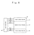
- symbol 40 denotes a shift register.
- the shift register 40 is connected to all the scanning lines G1, G2, ⁇ Gn-1, Gn, Gn+1 ⁇ of the LCD panel 30.
- a shift pulse is inputted from an input 41 to the shift register 40, and its shift pulse is transferred in a direction of an arrow Y1, in response to a shift clock (not shown). That is, the shift register 40 outputs the scanning signals VG1, VG2, ⁇ , VGn-1, VGn, VGn+1 ⁇ to the respective scanning lines Gl, G2, ⁇ Gn-1, Gn, Gn+1 ⁇ at a predetermined timing.
- a switch 42 is mounted between the two scanning lines Gn-1, Gn corresponding to a boundary between the first display region 31 and the second display region 32, in the shift register 40.
- the switch 42 is turned off, the shift pulse transferred in the direction of the arrow Y1 from the input 41 is not transferred on and after the scanning lines Gn, Gn+1 ⁇ .
- a controller (not shown) is mounted in the shift register 40. This controller counts the predetermined timings (shift clocks), and detects the number of frames FT at this time (which number of frame FT) in accordance with the count result. In the example shown in Fig. 3, the controller turns the switch 42 on, in the first and fourth frames FT. Thus, the scanning signals VG1, VG2, ⁇ , VGn-1, VGn, VGn+1 ⁇ are outputted to each of all the scanning lines G1, G2, ⁇ Gn-1, Gn, Gn+1 ⁇ at a predetermined timing. The controller turns the switch 42 off, in the second and third frames FT.
Landscapes
- Engineering & Computer Science (AREA)
- Theoretical Computer Science (AREA)
- Physics & Mathematics (AREA)
- Computer Hardware Design (AREA)
- General Physics & Mathematics (AREA)
- Crystallography & Structural Chemistry (AREA)
- Chemical & Material Sciences (AREA)
- Liquid Crystal Display Device Control (AREA)
- Liquid Crystal (AREA)
- Control Of Indicators Other Than Cathode Ray Tubes (AREA)
- Shift Register Type Memory (AREA)
- Devices For Indicating Variable Information By Combining Individual Elements (AREA)
- Electroluminescent Light Sources (AREA)
Abstract
Description
of the two regions, the other region has a voltage non-application period and a non-selective voltage application period at a predetermined cycle. Also, the same voltage as the signal voltage applied to the signal electrode of the selective scan region is applied to the signal electrode of the region on which the selective scan is not performed, in the non-selective voltage application period.
a plurality of scanning lines to which a plurality of scanning signals are inputted, respectively; a plurality of signal lines to which a plurality of display signals are inputted, respectively; a plurality of capacitance sections respectively provided through a plurality of switching elements at a plurality of intersections of the plurality of scanning lines and the plurality of signal lines; and a display section including the plurality of capacitance sections, and wherein the display section is divided into first, second and third display regions by two virtual lines parallel to at least one of the plurality of scanning lines, and wherein the plurality of scanning signals are inputted at first intervals to a first group of the scanning lines corresponding to the first display region of the plurality of scanning lines, and wherein the plurality of scanning signals are inputted at second intervals to a second group of the scanning lines corresponding to the second display region of the plurality of scanning lines, and wherein the plurality of scanning signals are inputted at third intervals to a third group of the scanning lines corresponding to the third display region of the plurality of scanning lines, and wherein at least one of the first, second and third intervals is different from a remaining one in a case that the at least one is withdrawn from the first, second and third intervals.
to carry out picture display (a middle between a static picture and a first display region) in which picture change is smaller than that of a dynamic picture of the first display region (Since an accumulation voltage is dropped with elapsing time, the contrast of a picture may be dropped).
of the condition in which the scanning signal is not merely inputted to the scanning line may cause a direct current voltage to be applied to the liquid crystal and result in the deterioration phenomenon such as the change of the material property and the drop of the specific resistance and the like.
may occur that a picture corresponding to a lengthened write period (this picture has the picture change smaller than that of the picture of the
if a record medium such as a television broadcast, a movie or the like is reproduced, a difference of an aspect ratio on a screen (4:3 and 16:9) and the like cause black portions to be induced in a top and a bottom of the screen, and a dynamic picture can-not be displayed on the black portions. This embodiment is not limited to the above-mentioned portable electronic apparatus, and it can be applied to various displays including television.
Claims (18)
- A display apparatus, comprising:a plurality of scanning lines (G) to which a plurality of scanning signals (VG) are inputted, respectively;a plurality of signal lines (S) to which a plurality of display signals (VS) are inputted, respectively;a plurality of capacitance sections (22) respectively provided through a plurality of switching elements (20) at a plurality of intersections of said plurality of scanning lines (G) and said plurality of signal lines (S); anda display section (30) including said plurality of capacitance sections (22),wherein said display section (30) is divided into first and second display regions (31, 32) by a virtual line parallel to at least one of said plurality of scanning lines (G), andwherein said plurality of scanning signals (VG1∼VGn-1) are inputted at first intervals to a first group of the scanning lines (G1∼Gn-1) corresponding to said first display region (31) of said plurality of scanning lines (G), andwherein said plurality of scanning signals (VGn, VGn+1···) are inputted at second intervals different from said first intervals to a second group of the scanning lines (Gn, Gn+1···) corresponding to said second display region (32) of said plurality of scanning lines (G).
- The display apparatus according to Claim 1, wherein said first intervals are selected such that said plurality of capacitance sections (22) of said first display region (31) are driven at alternating currents, and
wherein said second intervals are selected such that said plurality of capacitance sections (22) of said second display region (32) are driven at alternating currents. - The display apparatus according to Claim 1 or 2, wherein when said plurality of scanning signals (VGn, VGn+1···) are inputted to said second group of the scanning lines (Gn, Gn+1···), and the plurality of display signals (VS) inputted to said plurality of capacitance sections (22) of said second display region (32) have amplitudes substantially identical with each other.
- The display apparatus according to any one of Claims 1 to 3, wherein when said plurality of scanning signals (VGn, VGn+1···) are not inputted to said second group of the scanning lines (Gn, Gn+1···) based on a difference between said first and second intervals, a plurality of specific display signals (VS) having amplitudes substantially identical with said amplitudes of said plurality of display signals (VS) inputted to said plurality of capacitance sections (22) of said second display region (32) when said plurality of scanning signals (VGn, VGn+1···) are inputted to said second group of the scanning lines (Gn, Gn+1···), are outputted to said plurality of signal lines (S) at the same timings as when said plurality of scanning signals (VGn, VGn+1···) are inputted to said second group of the scanning lines (Gn, Gn+1···).
- The display apparatus according to Claim 4, wherein said amplitudes of said plurality of specific display signals (VS) are substantially zero.
- The display apparatus according to any one of Claims 1 to 4, wherein when said plurality of scanning signals (VGn, VGn+1···) are not inputted to said second group of the scanning lines (Gn, Gn+1···) based on a difference between said first and second intervals, potentials of said plurality of signal lines (S) are dropped at the same timings as when said plurality of scanning signals (VGn, VGn+1···) are inputted to said second group of the scanning lines (Gn, Gn+1···).
- The display apparatus according to any one of Claims 1 to 4, wherein when said plurality of scanning signals (VGn, VGn+1···) are not inputted to said second group of the scanning lines (Gn, Gn+1···) based on a difference between said first and second intervals, said plurality of signal lines (S) are in floating states at the same timings as when said plurality of scanning signals (VGn, VGn+1···) are inputted to said second group of the scanning lines (Gn, Gn+1···).
- The display apparatus according to any one of Claims 1 to 7, wherein when said plurality of scanning signals (VGn, VGn+1···) are not inputted to said second group of the scanning lines (Gn, Gn+1···) based on a difference between said first and second intervals, potentials of said second group of the scanning lines (Gn, Gn+1···) are dropped at the same timings as when said plurality of scanning signals (VGn, VGn+1···) are inputted to said second group of the scanning lines (Gn, Gn+1 ···).
- The display apparatus according to any one of Claims 1 to 8, further comprising:a first shift register supplying said plurality of scanning signals (VG1∼VGn-1) to said first group of the scanning lines (G1∼Gn-1) by transferring a first input signal one by one; anda second shift register supplying said plurality of scanning signals (VGn, VGn+1···) to said second group of the scanning lines (Gn, Gn+1 ···) by transferring a second input signal one by one.
- The display apparatus according to any one of Claims 1 to 8, further comprising:a shift register (40) supplying said plurality of scanning lines (G) to said plurality of scanning signals (VG) by transferring an input signal one by one, andwherein said shift register (40) has a switch (42) to stop transferring said input signal such that said plurality of scanning signals (VG1 ∼VGn-1) are supplied to said first group of the scanning lines (G1∼Gn-1) and said plurality of scanning signals (VGn, VGn+1···) are not supplied to said second group of the scanning lines (Gn, Gn+1···).
- The display apparatus according to Claim 10, wherein said input signal is transferred in a predetermined direction (Y1) in said shift register (40), andwherein a first input section (41) inputting said input signal is provided in the most upstream in said predetermined direction (Y1) of said first group of the scanning lines (G1∼Gn-1) in said shift register (40), andwherein a second input section (43) inputting said input signal is provided in the most upstream in said predetermined direction (Y1) of said second group of the scanning lines (Gn, Gn+1···) in said shift register (40).
- The display apparatus according to Claim 10 or 11, wherein each of said first and second intervals corresponds to a multiple of a period (FT) of a frame when a single image is displayed in said display section (30), and
wherein said display apparatus further comprises:
a control section detecting the number of said frames to switch between an ON state and an OFF state of said switch (42) based on the detected result. - The display apparatus according to any one of Claims 1 to 12, wherein said switching element (20) is one of a TFT (Thin-Film-Transistor) type and an MIM (Metal-Insulator-Metal) type.
- The display apparatus according to any one of Claims 1 to 13, wherein said display apparatus is provided on a single substrate.
- A driving method of a display apparatus, comprising:(a) providing a plurality of scanning lines (G) to which a plurality of scanning signals (VG) are inputted, respectively;(b) providing a plurality of signal lines (S) to which a plurality of display signals (VS) are inputted, respectively;(c) providing a plurality of capacitance sections (22) respectively provided through a plurality of switching elements (20) at a plurality of intersections of said plurality of scanning lines (G) and said plurality of signal lines (S);(d) providing a display section (30) including said plurality of capacitance sections (22);(e) dividing said display section (30) into first and second display regions (31, 32) by a virtual line parallel to at least one of said plurality of scanning lines (G);(f) inputting said plurality of scanning signals (VG1∼VGn-1) at first intervals to a first group of the scanning lines (G1∼Gn-1) corresponding to said first display region (31) of said plurality of scanning lines (G); and(g) inputting said plurality of scanning signals (VGn, VGn+1···) at second intervals different from said first intervals to a second group of the scanning lines (Gn, Gn+1···) corresponding to said second display region (32) of said plurality of scanning lines (G).
- A driving method of a display apparatus according to Claim 15, wherein said first intervals are selected such that said plurality of capacitance sections (22) of said first display region (31) are driven at alternating currents, and wherein said second intervals are selected such that said plurality of capacitance sections (22) of said second display region (32) are driven at alternating currents.
- A driving method of a display apparatus according to Claim 15 or 16, wherein when said plurality of scanning signals (VGn, VGn+1···) are inputted to said second group of the scanning lines (Gn, Gn+1···), said plurality of display signals (VS) inputted to said plurality of capacitance sections (22) of said second display region (32) have amplitudes substantially identical with each other.
- A driving method of a display apparatus according to any one of Claims 15 to 17, wherein when said plurality of scanning signals (VGn, VGn+1···) are not inputted to said second group of the scanning lines (Gn, Gn+1···) based on a difference between said first and second intervals, a plurality of specific display signals (VS) having amplitudes substantially identical with said amplitudes of said plurality of display signals (VS) inputted to said plurality of capacitance sections (22) of said second display region (32) when said plurality of scanning signals (VGn, VGn+1···) are inputted to said second group of the scanning lines (Gn, Gn+1···), are outputted to said plurality of signal lines (S) at the same timings as when said plurality of scanning signals (VGn, VGn+1···) are inputted to said second group of the scanning lines (Gn, Gn+1 ···).
Applications Claiming Priority (2)
| Application Number | Priority Date | Filing Date | Title |
|---|---|---|---|
| JP2000051706 | 2000-02-28 | ||
| JP2000051706A JP3498033B2 (en) | 2000-02-28 | 2000-02-28 | Display device, portable electronic device, and method of driving display device |
Publications (3)
| Publication Number | Publication Date |
|---|---|
| EP1134721A2 true EP1134721A2 (en) | 2001-09-19 |
| EP1134721A3 EP1134721A3 (en) | 2002-05-02 |
| EP1134721B1 EP1134721B1 (en) | 2005-08-17 |
Family
ID=18573322
Family Applications (1)
| Application Number | Title | Priority Date | Filing Date |
|---|---|---|---|
| EP01250055A Expired - Lifetime EP1134721B1 (en) | 2000-02-28 | 2001-02-21 | Display apparatus comprising two display regions and portable electronic apparatus that can reduce power consumption, and method of driving the same |
Country Status (5)
| Country | Link |
|---|---|
| US (1) | US6624801B2 (en) |
| EP (1) | EP1134721B1 (en) |
| JP (1) | JP3498033B2 (en) |
| KR (1) | KR100381883B1 (en) |
| TW (1) | TWI263966B (en) |
Cited By (15)
| Publication number | Priority date | Publication date | Assignee | Title |
|---|---|---|---|---|
| US6522319B1 (en) * | 1998-02-09 | 2003-02-18 | Seiko Epson Corporation | Electro-optical device and method for driving the same, liquid crystal device and method for driving the same, circuit for driving electro-optical device, and electronic device |
| EP1640953A2 (en) * | 2004-09-27 | 2006-03-29 | Idc, Llc | Method and system for reducing power consumption in a display |
| EP1640954A2 (en) | 2004-09-27 | 2006-03-29 | Idc, Llc | Controller and driver features for bi-stable display |
| CN100495519C (en) * | 2002-03-20 | 2009-06-03 | 株式会社日立显示器 | Driving method of active matrix liquid crystal display device |
| US7852542B2 (en) | 2004-08-27 | 2010-12-14 | Qualcomm Mems Technologies, Inc. | Current mode display driver circuit realization feature |
| US7957589B2 (en) | 2007-01-25 | 2011-06-07 | Qualcomm Mems Technologies, Inc. | Arbitrary power function using logarithm lookup table |
| US8085461B2 (en) | 2004-09-27 | 2011-12-27 | Qualcomm Mems Technologies, Inc. | Systems and methods of actuating MEMS display elements |
| US8344997B2 (en) | 2004-09-27 | 2013-01-01 | Qualcomm Mems Technologies, Inc. | Method and system for writing data to electromechanical display elements |
| US8405649B2 (en) | 2009-03-27 | 2013-03-26 | Qualcomm Mems Technologies, Inc. | Low voltage driver scheme for interferometric modulators |
| US8514169B2 (en) | 2004-09-27 | 2013-08-20 | Qualcomm Mems Technologies, Inc. | Apparatus and system for writing data to electromechanical display elements |
| CN103632640A (en) * | 2012-08-21 | 2014-03-12 | 联咏科技股份有限公司 | Driving device of liquid crystal display |
| EP3118844A4 (en) * | 2014-03-10 | 2018-02-28 | LG Display Co., Ltd. | Display device |
| US9959822B2 (en) | 2009-10-16 | 2018-05-01 | Semiconductor Energy Laboratory Co., Ltd. | Liquid crystal display device and electronic device including the liquid crystal display device |
| CN108169900A (en) * | 2016-12-07 | 2018-06-15 | 三星显示有限公司 | Display device |
| CN110890063A (en) * | 2019-11-22 | 2020-03-17 | 深圳市华星光电半导体显示技术有限公司 | Method and device for reducing power consumption of display panel |
Families Citing this family (62)
| Publication number | Priority date | Publication date | Assignee | Title |
|---|---|---|---|---|
| JP3572473B2 (en) | 1997-01-30 | 2004-10-06 | 株式会社ルネサステクノロジ | Liquid crystal display control device |
| JP2002156946A (en) * | 2000-11-16 | 2002-05-31 | Matsushita Electric Ind Co Ltd | Driving device of liquid crystal display panel |
| KR100733879B1 (en) * | 2000-12-30 | 2007-07-02 | 엘지.필립스 엘시디 주식회사 | LCD Display |
| JP3743503B2 (en) | 2001-05-24 | 2006-02-08 | セイコーエプソン株式会社 | Scan driving circuit, display device, electro-optical device, and scan driving method |
| JP3750734B2 (en) * | 2001-07-27 | 2006-03-01 | セイコーエプソン株式会社 | Scan line driving circuit, electro-optical device, electronic apparatus, and semiconductor device |
| TW519611B (en) * | 2001-08-01 | 2003-02-01 | Au Optronics Corp | Driving method of power-saving type thin film transistor |
| KR100429880B1 (en) * | 2001-09-25 | 2004-05-03 | 삼성전자주식회사 | Circuit and method for controlling LCD frame ratio and LCD system having the same |
| JP4190862B2 (en) * | 2001-12-18 | 2008-12-03 | シャープ株式会社 | Display device and driving method thereof |
| EP1518217A2 (en) | 2002-06-22 | 2005-03-30 | Koninklijke Philips Electronics N.V. | Circuit arrangement for a display device which can be operated in a partial mode |
| JP5494196B2 (en) * | 2002-09-30 | 2014-05-14 | セイコーエプソン株式会社 | Display device, electronic device, and projection display device |
| JP4256665B2 (en) * | 2002-11-15 | 2009-04-22 | 株式会社 日立ディスプレイズ | Image display device |
| JP2004240235A (en) * | 2003-02-07 | 2004-08-26 | Hitachi Ltd | LSI for display device |
| JP4074207B2 (en) * | 2003-03-10 | 2008-04-09 | 株式会社 日立ディスプレイズ | Liquid crystal display |
| TWI248600B (en) * | 2003-05-08 | 2006-02-01 | Ind Tech Res Inst | Apparatus and method for supplying the video signal with time-division multiplexing |
| JP4543632B2 (en) * | 2003-08-07 | 2010-09-15 | 日本電気株式会社 | Liquid crystal display device and liquid crystal display device driving method |
| KR100557092B1 (en) * | 2003-08-29 | 2006-03-03 | 삼성전자주식회사 | A mobile terminal for displaying a variable auxiliary display area and a method thereof |
| KR100621864B1 (en) * | 2003-11-18 | 2006-09-13 | 엘지.필립스 엘시디 주식회사 | Driving Method of LCD |
| JP2005156766A (en) * | 2003-11-25 | 2005-06-16 | Nec Corp | Display system and electronic apparatus using same |
| GB0402046D0 (en) * | 2004-01-29 | 2004-03-03 | Koninkl Philips Electronics Nv | Active matrix display device |
| TWI247168B (en) * | 2004-02-27 | 2006-01-11 | Au Optronics Corp | Liquid crystal display and ESD protection circuit thereon |
| JP2005301145A (en) * | 2004-04-15 | 2005-10-27 | Optrex Corp | Driving device for liquid crystal display device and liquid crystal display device |
| JP4581851B2 (en) * | 2004-07-27 | 2010-11-17 | セイコーエプソン株式会社 | Electro-optical device driving circuit and driving method, electro-optical device, and electronic apparatus |
| US7586484B2 (en) | 2004-09-27 | 2009-09-08 | Idc, Llc | Controller and driver features for bi-stable display |
| US7920135B2 (en) | 2004-09-27 | 2011-04-05 | Qualcomm Mems Technologies, Inc. | Method and system for driving a bi-stable display |
| US7948457B2 (en) | 2005-05-05 | 2011-05-24 | Qualcomm Mems Technologies, Inc. | Systems and methods of actuating MEMS display elements |
| US7920136B2 (en) | 2005-05-05 | 2011-04-05 | Qualcomm Mems Technologies, Inc. | System and method of driving a MEMS display device |
| JP4810910B2 (en) * | 2005-07-26 | 2011-11-09 | エプソンイメージングデバイス株式会社 | Electro-optical device, driving method, and electronic apparatus |
| CN101263548B (en) * | 2005-09-15 | 2010-05-26 | 夏普株式会社 | Image transmission device and display system using the same |
| US20080225033A1 (en) * | 2005-09-19 | 2008-09-18 | Koninklijke Philips Electronics, N.V. | Display Devices and Row Voltage Generation Circuits |
| JP4902185B2 (en) * | 2005-12-14 | 2012-03-21 | 株式会社 日立ディスプレイズ | Display device |
| US8391630B2 (en) | 2005-12-22 | 2013-03-05 | Qualcomm Mems Technologies, Inc. | System and method for power reduction when decompressing video streams for interferometric modulator displays |
| US8194056B2 (en) | 2006-02-09 | 2012-06-05 | Qualcomm Mems Technologies Inc. | Method and system for writing data to MEMS display elements |
| US8049713B2 (en) | 2006-04-24 | 2011-11-01 | Qualcomm Mems Technologies, Inc. | Power consumption optimized display update |
| JP2008107570A (en) * | 2006-10-25 | 2008-05-08 | Pioneer Electronic Corp | Display controller, display apparatus, and display control method |
| JP2008185996A (en) * | 2007-01-31 | 2008-08-14 | Casio Comput Co Ltd | Liquid crystal display device and drive control method thereof |
| JP2008250093A (en) * | 2007-03-30 | 2008-10-16 | Sony Corp | Display device and driving method thereof |
| CN101802903A (en) * | 2007-10-04 | 2010-08-11 | 夏普株式会社 | Display device and display device drive method |
| US20090251403A1 (en) * | 2008-04-07 | 2009-10-08 | Himax Technologies Limited | Liquid crystal display panel |
| TWI392908B (en) * | 2008-05-16 | 2013-04-11 | Au Optronics Corp | Display apparatus |
| GB0814079D0 (en) * | 2008-08-01 | 2008-09-10 | Liquavista Bv | Electrowetting system |
| JP2010156856A (en) * | 2008-12-27 | 2010-07-15 | Seiko Epson Corp | Electrooptical apparatus and electronic device |
| US8405770B2 (en) * | 2009-03-12 | 2013-03-26 | Intellectual Ventures Fund 83 Llc | Display of video with motion |
| US8736590B2 (en) | 2009-03-27 | 2014-05-27 | Qualcomm Mems Technologies, Inc. | Low voltage driver scheme for interferometric modulators |
| JP4677498B2 (en) * | 2009-07-13 | 2011-04-27 | 株式会社日立製作所 | Display device |
| JP2011030081A (en) * | 2009-07-28 | 2011-02-10 | Sony Corp | Display device, display system, display method and program |
| JP4813606B2 (en) * | 2010-02-01 | 2011-11-09 | ソニー株式会社 | Display device |
| CN102222456B (en) * | 2010-04-16 | 2013-05-29 | 北京京东方光电科技有限公司 | Common electrode driving method, circuit and liquid crystal displayer |
| WO2012002258A1 (en) * | 2010-06-30 | 2012-01-05 | シャープ株式会社 | Display device, method for controlling the display device, program, and recording medium |
| US9607537B2 (en) * | 2010-12-23 | 2017-03-28 | Microsoft Technology Licensing, Llc | Display region refresh |
| WO2013080985A1 (en) * | 2011-11-30 | 2013-06-06 | シャープ株式会社 | Control unit, display device including control unit, and control method |
| TWI462075B (en) * | 2012-01-20 | 2014-11-21 | Hung Ta Liu | A driving method and a display structure using the driving method |
| US9401119B2 (en) * | 2012-06-15 | 2016-07-26 | Sharp Kabushiki Kaisha | Display device and display method |
| CN103839523A (en) * | 2012-11-20 | 2014-06-04 | 北京京东方光电科技有限公司 | Apparatus and method for reducing power consumption of liquid crystal display panel |
| US10565925B2 (en) * | 2014-02-07 | 2020-02-18 | Samsung Electronics Co., Ltd. | Full color display with intrinsic transparency |
| KR102276330B1 (en) * | 2014-03-10 | 2021-07-13 | 엘지디스플레이 주식회사 | Display device and method of drving the same |
| CN106104664B (en) * | 2014-03-10 | 2019-05-03 | 乐金显示有限公司 | Display device and driving method thereof |
| KR101698930B1 (en) * | 2014-11-11 | 2017-01-23 | 삼성전자 주식회사 | Display driving device, display device and Opertaing method thereof |
| KR102290559B1 (en) * | 2015-02-02 | 2021-08-18 | 삼성디스플레이 주식회사 | Display device and electronic device having the same |
| TWI596595B (en) | 2016-06-02 | 2017-08-21 | 凌巨科技股份有限公司 | Display apparatus and driving method of display panel thereof |
| KR102740962B1 (en) * | 2017-01-10 | 2024-12-12 | 삼성디스플레이 주식회사 | Display device and driving method thereof |
| CN109003584B (en) * | 2018-07-24 | 2020-06-26 | 惠科股份有限公司 | Display device and display panel thereof |
| JP7767392B2 (en) * | 2021-03-25 | 2025-11-11 | 株式会社半導体エネルギー研究所 | Display device and electronic device |
Family Cites Families (26)
| Publication number | Priority date | Publication date | Assignee | Title |
|---|---|---|---|---|
| JPS63243921A (en) | 1987-03-31 | 1988-10-11 | Matsushita Electric Ind Co Ltd | liquid crystal display device |
| JP2744841B2 (en) * | 1990-09-06 | 1998-04-28 | キヤノン株式会社 | Electronics |
| JPH0695621A (en) | 1992-09-16 | 1994-04-08 | Fujitsu Ltd | Liquid crystal display controller and liquid crystal display device |
| JP2735451B2 (en) * | 1993-01-05 | 1998-04-02 | 日本電気株式会社 | Multi-scan type liquid crystal display device |
| US5828367A (en) * | 1993-10-21 | 1998-10-27 | Rohm Co., Ltd. | Display arrangement |
| JPH07152340A (en) * | 1993-11-30 | 1995-06-16 | Rohm Co Ltd | Display device |
| JP3476241B2 (en) * | 1994-02-25 | 2003-12-10 | 株式会社半導体エネルギー研究所 | Display method of active matrix type display device |
| JPH07281632A (en) | 1994-04-04 | 1995-10-27 | Casio Comput Co Ltd | Liquid crystal display |
| JP3298301B2 (en) * | 1994-04-18 | 2002-07-02 | カシオ計算機株式会社 | Liquid crystal drive |
| JP3027298B2 (en) * | 1994-05-31 | 2000-03-27 | シャープ株式会社 | Liquid crystal display with backlight control function |
| JP3322327B2 (en) * | 1995-03-14 | 2002-09-09 | シャープ株式会社 | Drive circuit |
| JP3234131B2 (en) * | 1995-06-23 | 2001-12-04 | 株式会社東芝 | Liquid crystal display |
| JP3694527B2 (en) * | 1995-09-20 | 2005-09-14 | 株式会社 日立製作所 | Image display device |
| CN1162736C (en) | 1995-12-14 | 2004-08-18 | 精工爱普生株式会社 | Display device driving method, display device and electronic device |
| GB9525638D0 (en) * | 1995-12-15 | 1996-02-14 | Philips Electronics Nv | Matrix display devices |
| EP0797182A1 (en) * | 1996-03-19 | 1997-09-24 | Hitachi, Ltd. | Active matrix LCD with data holding circuit in each pixel |
| US5867140A (en) * | 1996-11-27 | 1999-02-02 | Motorola, Inc. | Display system and circuit therefor |
| JP3572473B2 (en) * | 1997-01-30 | 2004-10-06 | 株式会社ルネサステクノロジ | Liquid crystal display control device |
| GB2323958A (en) * | 1997-04-04 | 1998-10-07 | Sharp Kk | Active matrix devices |
| JPH11184434A (en) * | 1997-12-19 | 1999-07-09 | Seiko Epson Corp | Liquid crystal devices and electronic equipment |
| EP0974952B1 (en) * | 1998-02-09 | 2007-02-28 | Seiko Epson Corporation | Electro-optical device and method for driving the same, liquid crystal device and method for driving the same, circuit for driving electro-optical device, and electronic device |
| JPH11271709A (en) * | 1998-03-20 | 1999-10-08 | Toshiba Corp | Display device |
| JPH11311980A (en) | 1998-04-28 | 1999-11-09 | Hitachi Ltd | Liquid crystal display control device and liquid crystal display device |
| JP4050383B2 (en) | 1998-04-30 | 2008-02-20 | セイコーエプソン株式会社 | Liquid crystal display device driving method, liquid crystal display device, and electronic apparatus |
| JP2000020015A (en) * | 1998-07-03 | 2000-01-21 | Toshiba Corp | Image display apparatus and method |
| JP2001202053A (en) * | 1999-11-09 | 2001-07-27 | Matsushita Electric Ind Co Ltd | Display device and portable information terminal |
-
2000
- 2000-02-28 JP JP2000051706A patent/JP3498033B2/en not_active Expired - Fee Related
-
2001
- 2001-02-20 TW TW090103864A patent/TWI263966B/en not_active IP Right Cessation
- 2001-02-21 EP EP01250055A patent/EP1134721B1/en not_active Expired - Lifetime
- 2001-02-26 US US09/791,803 patent/US6624801B2/en not_active Expired - Lifetime
- 2001-02-28 KR KR10-2001-0010429A patent/KR100381883B1/en not_active Expired - Lifetime
Cited By (23)
| Publication number | Priority date | Publication date | Assignee | Title |
|---|---|---|---|---|
| US6900788B2 (en) | 1998-02-09 | 2005-05-31 | Seiko Epson Corporation | Electrooptical apparatus and driving method therefor, liquid crystal display apparatus and driving method therefor, electrooptical apparatus and driving circuit therefor, and electronic equipment |
| US6522319B1 (en) * | 1998-02-09 | 2003-02-18 | Seiko Epson Corporation | Electro-optical device and method for driving the same, liquid crystal device and method for driving the same, circuit for driving electro-optical device, and electronic device |
| CN100495519C (en) * | 2002-03-20 | 2009-06-03 | 株式会社日立显示器 | Driving method of active matrix liquid crystal display device |
| US7852542B2 (en) | 2004-08-27 | 2010-12-14 | Qualcomm Mems Technologies, Inc. | Current mode display driver circuit realization feature |
| US8344997B2 (en) | 2004-09-27 | 2013-01-01 | Qualcomm Mems Technologies, Inc. | Method and system for writing data to electromechanical display elements |
| US8514169B2 (en) | 2004-09-27 | 2013-08-20 | Qualcomm Mems Technologies, Inc. | Apparatus and system for writing data to electromechanical display elements |
| EP1640954A2 (en) | 2004-09-27 | 2006-03-29 | Idc, Llc | Controller and driver features for bi-stable display |
| EP1640954A3 (en) * | 2004-09-27 | 2008-10-29 | Idc, Llc | Controller and driver features for bi-stable display |
| US8085461B2 (en) | 2004-09-27 | 2011-12-27 | Qualcomm Mems Technologies, Inc. | Systems and methods of actuating MEMS display elements |
| US8243014B2 (en) | 2004-09-27 | 2012-08-14 | Qualcomm Mems Technologies, Inc. | Method and system for reducing power consumption in a display |
| EP1640953A2 (en) * | 2004-09-27 | 2006-03-29 | Idc, Llc | Method and system for reducing power consumption in a display |
| US8471808B2 (en) | 2004-09-27 | 2013-06-25 | Qualcomm Mems Technologies, Inc. | Method and device for reducing power consumption in a display |
| US7957589B2 (en) | 2007-01-25 | 2011-06-07 | Qualcomm Mems Technologies, Inc. | Arbitrary power function using logarithm lookup table |
| US8405649B2 (en) | 2009-03-27 | 2013-03-26 | Qualcomm Mems Technologies, Inc. | Low voltage driver scheme for interferometric modulators |
| US9959822B2 (en) | 2009-10-16 | 2018-05-01 | Semiconductor Energy Laboratory Co., Ltd. | Liquid crystal display device and electronic device including the liquid crystal display device |
| US10565946B2 (en) | 2009-10-16 | 2020-02-18 | Semiconductor Energy Laboratory Co., Ltd. | Liquid crystal display device and electronic device including the liquid crystal display device |
| CN103632640A (en) * | 2012-08-21 | 2014-03-12 | 联咏科技股份有限公司 | Driving device of liquid crystal display |
| EP3118844A4 (en) * | 2014-03-10 | 2018-02-28 | LG Display Co., Ltd. | Display device |
| CN108169900A (en) * | 2016-12-07 | 2018-06-15 | 三星显示有限公司 | Display device |
| US11100843B2 (en) | 2016-12-07 | 2021-08-24 | Samsung Display Co., Ltd. | Display device having a plurality of display areas |
| CN108169900B (en) * | 2016-12-07 | 2022-07-05 | 三星显示有限公司 | display device |
| US11594168B2 (en) | 2016-12-07 | 2023-02-28 | Samsung Display Co., Ltd. | Display device having a plurality of pixel areas |
| CN110890063A (en) * | 2019-11-22 | 2020-03-17 | 深圳市华星光电半导体显示技术有限公司 | Method and device for reducing power consumption of display panel |
Also Published As
| Publication number | Publication date |
|---|---|
| KR100381883B1 (en) | 2003-04-26 |
| US6624801B2 (en) | 2003-09-23 |
| JP2001242818A (en) | 2001-09-07 |
| EP1134721B1 (en) | 2005-08-17 |
| EP1134721A3 (en) | 2002-05-02 |
| TWI263966B (en) | 2006-10-11 |
| JP3498033B2 (en) | 2004-02-16 |
| KR20010085723A (en) | 2001-09-07 |
| US20010017611A1 (en) | 2001-08-30 |
Similar Documents
| Publication | Publication Date | Title |
|---|---|---|
| US6624801B2 (en) | Display apparatus and portable electronic apparatus that can reduce consumptive power, and method of driving display apparatus | |
| CN101675374B (en) | Liquid crystal display device | |
| KR100511809B1 (en) | Liquid crystal display device and driving method of the same | |
| EP0974952A1 (en) | Electro-optical device and method for driving the same, liquid crystal device and method for driving the same, circuit for driving electro-optical device, and electronic device | |
| KR100810289B1 (en) | Active matrix type bistable display | |
| US20050253829A1 (en) | Display device and display device driving method | |
| US20040183768A1 (en) | Liquid crystal display device and method for driving the same | |
| KR100949634B1 (en) | Electro-optical devices, drive circuits and electronic devices | |
| JP2004317785A (en) | Driving method of electro-optical device, electro-optical device, and electronic apparatus | |
| EP0767449A2 (en) | Method and circuit for driving active matrix liquid crystal panel with control of the average driving voltage | |
| JPH08251518A (en) | Drive circuit | |
| US20090219237A1 (en) | Electro-optical device, driving method thereof, and electronic apparatus | |
| JP5346379B2 (en) | Pixel circuit and display device | |
| US20060187164A1 (en) | Liquid crystal display device performing dot inversion and method of driving the same | |
| KR20050017401A (en) | Liquid crystal display device | |
| KR100389027B1 (en) | Liquid Crystal Display and Driving Method Thereof | |
| CN100385495C (en) | Power saving circuit and method | |
| KR100848953B1 (en) | Gate driving circuit of liquid crystal display device | |
| KR20050106125A (en) | Active matrix displays and drive control methods | |
| JP4270442B2 (en) | Display device and driving method thereof | |
| JP4957169B2 (en) | Electro-optical device, scanning line driving circuit, and electronic apparatus | |
| JP2002149120A (en) | Liquid crystal display device, information processing device, method for stopping voltage supply of liquid crystal display device, medium, and information aggregate | |
| JP2010044295A (en) | Electrooptical apparatus, its driving method, and electronic device | |
| KR100825424B1 (en) | DSD LC drive method and driving device | |
| JPH0363077B2 (en) |
Legal Events
| Date | Code | Title | Description |
|---|---|---|---|
| PUAI | Public reference made under article 153(3) epc to a published international application that has entered the european phase |
Free format text: ORIGINAL CODE: 0009012 |
|
| AK | Designated contracting states |
Kind code of ref document: A2 Designated state(s): FI NL Kind code of ref document: A2 Designated state(s): AT BE CH CY DE DK ES FI FR GB GR IE IT LI LU MC NL PT SE TR |
|
| AX | Request for extension of the european patent |
Free format text: AL;LT;LV;MK;RO;SI |
|
| PUAL | Search report despatched |
Free format text: ORIGINAL CODE: 0009013 |
|
| AK | Designated contracting states |
Kind code of ref document: A3 Designated state(s): AT BE CH CY DE DK ES FI FR GB GR IE IT LI LU MC NL PT SE TR |
|
| AX | Request for extension of the european patent |
Free format text: AL;LT;LV;MK;RO;SI |
|
| 17P | Request for examination filed |
Effective date: 20020513 |
|
| 17Q | First examination report despatched |
Effective date: 20020903 |
|
| AKX | Designation fees paid |
Free format text: FI NL |
|
| REG | Reference to a national code |
Ref country code: DE Ref legal event code: 8566 |
|
| RAP1 | Party data changed (applicant data changed or rights of an application transferred) |
Owner name: NEC LCD TECHNOLOGIES, LTD. |
|
| GRAP | Despatch of communication of intention to grant a patent |
Free format text: ORIGINAL CODE: EPIDOSNIGR1 |
|
| GRAS | Grant fee paid |
Free format text: ORIGINAL CODE: EPIDOSNIGR3 |
|
| GRAA | (expected) grant |
Free format text: ORIGINAL CODE: 0009210 |
|
| AK | Designated contracting states |
Kind code of ref document: B1 Designated state(s): FI NL |
|
| PLBE | No opposition filed within time limit |
Free format text: ORIGINAL CODE: 0009261 |
|
| STAA | Information on the status of an ep patent application or granted ep patent |
Free format text: STATUS: NO OPPOSITION FILED WITHIN TIME LIMIT |
|
| 26N | No opposition filed |
Effective date: 20060518 |
|
| REG | Reference to a national code |
Ref country code: NL Ref legal event code: SD Effective date: 20100310 |
|
| REG | Reference to a national code |
Ref country code: NL Ref legal event code: SD Effective date: 20130329 |
|
| PGFP | Annual fee paid to national office [announced via postgrant information from national office to epo] |
Ref country code: NL Payment date: 20150125 Year of fee payment: 15 |
|
| PGFP | Annual fee paid to national office [announced via postgrant information from national office to epo] |
Ref country code: FI Payment date: 20150209 Year of fee payment: 15 |
|
| PG25 | Lapsed in a contracting state [announced via postgrant information from national office to epo] |
Ref country code: FI Free format text: LAPSE BECAUSE OF NON-PAYMENT OF DUE FEES Effective date: 20160221 |
|
| REG | Reference to a national code |
Ref country code: NL Ref legal event code: MM Effective date: 20160301 |
|
| PG25 | Lapsed in a contracting state [announced via postgrant information from national office to epo] |
Ref country code: NL Free format text: LAPSE BECAUSE OF NON-PAYMENT OF DUE FEES Effective date: 20160301 |