EP1132948A2 - Substrate holding device, semiconductor manufacturing apparatus and device manufacturing device - Google Patents
Substrate holding device, semiconductor manufacturing apparatus and device manufacturing device Download PDFInfo
- Publication number
- EP1132948A2 EP1132948A2 EP01302152A EP01302152A EP1132948A2 EP 1132948 A2 EP1132948 A2 EP 1132948A2 EP 01302152 A EP01302152 A EP 01302152A EP 01302152 A EP01302152 A EP 01302152A EP 1132948 A2 EP1132948 A2 EP 1132948A2
- Authority
- EP
- European Patent Office
- Prior art keywords
- plate
- base member
- substrate
- holding device
- projection
- Prior art date
- Legal status (The legal status is an assumption and is not a legal conclusion. Google has not performed a legal analysis and makes no representation as to the accuracy of the status listed.)
- Granted
Links
Images






Classifications
-
- H—ELECTRICITY
- H10—SEMICONDUCTOR DEVICES; ELECTRIC SOLID-STATE DEVICES NOT OTHERWISE PROVIDED FOR
- H10P—GENERIC PROCESSES OR APPARATUS FOR THE MANUFACTURE OR TREATMENT OF DEVICES COVERED BY CLASS H10
- H10P72/00—Handling or holding of wafers, substrates or devices during manufacture or treatment thereof
- H10P72/70—Handling or holding of wafers, substrates or devices during manufacture or treatment thereof for supporting or gripping
- H10P72/76—Handling or holding of wafers, substrates or devices during manufacture or treatment thereof for supporting or gripping using mechanical means, e.g. clamps or pinches
- H10P72/7604—Handling or holding of wafers, substrates or devices during manufacture or treatment thereof for supporting or gripping using mechanical means, e.g. clamps or pinches the wafers being placed on a susceptor, stage or support
- H10P72/7614—Handling or holding of wafers, substrates or devices during manufacture or treatment thereof for supporting or gripping using mechanical means, e.g. clamps or pinches the wafers being placed on a susceptor, stage or support characterised by a plurality of individual support members, e.g. support posts or protrusions
-
- G—PHYSICS
- G03—PHOTOGRAPHY; CINEMATOGRAPHY; ANALOGOUS TECHNIQUES USING WAVES OTHER THAN OPTICAL WAVES; ELECTROGRAPHY; HOLOGRAPHY
- G03F—PHOTOMECHANICAL PRODUCTION OF TEXTURED OR PATTERNED SURFACES, e.g. FOR PRINTING, FOR PROCESSING OF SEMICONDUCTOR DEVICES; MATERIALS THEREFOR; ORIGINALS THEREFOR; APPARATUS SPECIALLY ADAPTED THEREFOR
- G03F7/00—Photomechanical, e.g. photolithographic, production of textured or patterned surfaces, e.g. printing surfaces; Materials therefor, e.g. comprising photoresists; Apparatus specially adapted therefor
- G03F7/70—Microphotolithographic exposure; Apparatus therefor
- G03F7/70691—Handling of masks or workpieces
- G03F7/707—Chucks, e.g. chucking or un-chucking operations or structural details
-
- G—PHYSICS
- G03—PHOTOGRAPHY; CINEMATOGRAPHY; ANALOGOUS TECHNIQUES USING WAVES OTHER THAN OPTICAL WAVES; ELECTROGRAPHY; HOLOGRAPHY
- G03F—PHOTOMECHANICAL PRODUCTION OF TEXTURED OR PATTERNED SURFACES, e.g. FOR PRINTING, FOR PROCESSING OF SEMICONDUCTOR DEVICES; MATERIALS THEREFOR; ORIGINALS THEREFOR; APPARATUS SPECIALLY ADAPTED THEREFOR
- G03F7/00—Photomechanical, e.g. photolithographic, production of textured or patterned surfaces, e.g. printing surfaces; Materials therefor, e.g. comprising photoresists; Apparatus specially adapted therefor
- G03F7/70—Microphotolithographic exposure; Apparatus therefor
- G03F7/70691—Handling of masks or workpieces
- G03F7/707—Chucks, e.g. chucking or un-chucking operations or structural details
- G03F7/70708—Chucks, e.g. chucking or un-chucking operations or structural details being electrostatic; Electrostatically deformable vacuum chucks
-
- G—PHYSICS
- G03—PHOTOGRAPHY; CINEMATOGRAPHY; ANALOGOUS TECHNIQUES USING WAVES OTHER THAN OPTICAL WAVES; ELECTROGRAPHY; HOLOGRAPHY
- G03F—PHOTOMECHANICAL PRODUCTION OF TEXTURED OR PATTERNED SURFACES, e.g. FOR PRINTING, FOR PROCESSING OF SEMICONDUCTOR DEVICES; MATERIALS THEREFOR; ORIGINALS THEREFOR; APPARATUS SPECIALLY ADAPTED THEREFOR
- G03F7/00—Photomechanical, e.g. photolithographic, production of textured or patterned surfaces, e.g. printing surfaces; Materials therefor, e.g. comprising photoresists; Apparatus specially adapted therefor
- G03F7/70—Microphotolithographic exposure; Apparatus therefor
- G03F7/70691—Handling of masks or workpieces
- G03F7/70733—Handling masks and workpieces, e.g. exchange of workpiece or mask, transport of workpiece or mask
- G03F7/7075—Handling workpieces outside exposure position, e.g. SMIF box
-
- G—PHYSICS
- G03—PHOTOGRAPHY; CINEMATOGRAPHY; ANALOGOUS TECHNIQUES USING WAVES OTHER THAN OPTICAL WAVES; ELECTROGRAPHY; HOLOGRAPHY
- G03F—PHOTOMECHANICAL PRODUCTION OF TEXTURED OR PATTERNED SURFACES, e.g. FOR PRINTING, FOR PROCESSING OF SEMICONDUCTOR DEVICES; MATERIALS THEREFOR; ORIGINALS THEREFOR; APPARATUS SPECIALLY ADAPTED THEREFOR
- G03F7/00—Photomechanical, e.g. photolithographic, production of textured or patterned surfaces, e.g. printing surfaces; Materials therefor, e.g. comprising photoresists; Apparatus specially adapted therefor
- G03F7/70—Microphotolithographic exposure; Apparatus therefor
- G03F7/708—Construction of apparatus, e.g. environment aspects, hygiene aspects or materials
- G03F7/70908—Hygiene, e.g. preventing apparatus pollution, mitigating effect of pollution or removing pollutants from apparatus
- G03F7/70925—Cleaning, i.e. actively freeing apparatus from pollutants, e.g. using plasma cleaning
-
- H—ELECTRICITY
- H10—SEMICONDUCTOR DEVICES; ELECTRIC SOLID-STATE DEVICES NOT OTHERWISE PROVIDED FOR
- H10P—GENERIC PROCESSES OR APPARATUS FOR THE MANUFACTURE OR TREATMENT OF DEVICES COVERED BY CLASS H10
- H10P72/00—Handling or holding of wafers, substrates or devices during manufacture or treatment thereof
- H10P72/06—Apparatus for monitoring, sorting, marking, testing or measuring
- H10P72/0606—Position monitoring, e.g. misposition detection or presence detection
- H10P72/0608—Position monitoring, e.g. misposition detection or presence detection of substrates stored in a container, a magazine, a carrier, a boat or the like
-
- H—ELECTRICITY
- H10—SEMICONDUCTOR DEVICES; ELECTRIC SOLID-STATE DEVICES NOT OTHERWISE PROVIDED FOR
- H10P—GENERIC PROCESSES OR APPARATUS FOR THE MANUFACTURE OR TREATMENT OF DEVICES COVERED BY CLASS H10
- H10P72/00—Handling or holding of wafers, substrates or devices during manufacture or treatment thereof
- H10P72/06—Apparatus for monitoring, sorting, marking, testing or measuring
- H10P72/0618—Apparatus for monitoring, sorting, marking, testing or measuring using identification means, e.g. labels on substrates or labels on containers
-
- H—ELECTRICITY
- H10—SEMICONDUCTOR DEVICES; ELECTRIC SOLID-STATE DEVICES NOT OTHERWISE PROVIDED FOR
- H10P—GENERIC PROCESSES OR APPARATUS FOR THE MANUFACTURE OR TREATMENT OF DEVICES COVERED BY CLASS H10
- H10P72/00—Handling or holding of wafers, substrates or devices during manufacture or treatment thereof
- H10P72/70—Handling or holding of wafers, substrates or devices during manufacture or treatment thereof for supporting or gripping
- H10P72/72—Handling or holding of wafers, substrates or devices during manufacture or treatment thereof for supporting or gripping using electrostatic chucks
-
- H—ELECTRICITY
- H10—SEMICONDUCTOR DEVICES; ELECTRIC SOLID-STATE DEVICES NOT OTHERWISE PROVIDED FOR
- H10P—GENERIC PROCESSES OR APPARATUS FOR THE MANUFACTURE OR TREATMENT OF DEVICES COVERED BY CLASS H10
- H10P72/00—Handling or holding of wafers, substrates or devices during manufacture or treatment thereof
- H10P72/70—Handling or holding of wafers, substrates or devices during manufacture or treatment thereof for supporting or gripping
- H10P72/76—Handling or holding of wafers, substrates or devices during manufacture or treatment thereof for supporting or gripping using mechanical means, e.g. clamps or pinches
- H10P72/7604—Handling or holding of wafers, substrates or devices during manufacture or treatment thereof for supporting or gripping using mechanical means, e.g. clamps or pinches the wafers being placed on a susceptor, stage or support
-
- H—ELECTRICITY
- H10—SEMICONDUCTOR DEVICES; ELECTRIC SOLID-STATE DEVICES NOT OTHERWISE PROVIDED FOR
- H10P—GENERIC PROCESSES OR APPARATUS FOR THE MANUFACTURE OR TREATMENT OF DEVICES COVERED BY CLASS H10
- H10P72/00—Handling or holding of wafers, substrates or devices during manufacture or treatment thereof
- H10P72/70—Handling or holding of wafers, substrates or devices during manufacture or treatment thereof for supporting or gripping
- H10P72/76—Handling or holding of wafers, substrates or devices during manufacture or treatment thereof for supporting or gripping using mechanical means, e.g. clamps or pinches
- H10P72/7604—Handling or holding of wafers, substrates or devices during manufacture or treatment thereof for supporting or gripping using mechanical means, e.g. clamps or pinches the wafers being placed on a susceptor, stage or support
- H10P72/7624—Handling or holding of wafers, substrates or devices during manufacture or treatment thereof for supporting or gripping using mechanical means, e.g. clamps or pinches the wafers being placed on a susceptor, stage or support characterised by the mechanical construction of the susceptor, stage or support
-
- H—ELECTRICITY
- H10—SEMICONDUCTOR DEVICES; ELECTRIC SOLID-STATE DEVICES NOT OTHERWISE PROVIDED FOR
- H10P—GENERIC PROCESSES OR APPARATUS FOR THE MANUFACTURE OR TREATMENT OF DEVICES COVERED BY CLASS H10
- H10P72/00—Handling or holding of wafers, substrates or devices during manufacture or treatment thereof
- H10P72/70—Handling or holding of wafers, substrates or devices during manufacture or treatment thereof for supporting or gripping
- H10P72/78—Handling or holding of wafers, substrates or devices during manufacture or treatment thereof for supporting or gripping using vacuum or suction, e.g. Bernoulli chucks
-
- H—ELECTRICITY
- H10—SEMICONDUCTOR DEVICES; ELECTRIC SOLID-STATE DEVICES NOT OTHERWISE PROVIDED FOR
- H10W—GENERIC PACKAGES, INTERCONNECTIONS, CONNECTORS OR OTHER CONSTRUCTIONAL DETAILS OF DEVICES COVERED BY CLASS H10
- H10W46/00—Marks applied to devices, e.g. for alignment or identification
- H10W46/201—Marks applied to devices, e.g. for alignment or identification located on the periphery of wafers, e.g. orientation notches or lot numbers
Definitions
- the present invention relates to a substrate holding device for holding a substrate (wafer) and an aligner or a semiconductor device manufacturing method using the substrate holding device.
- photosensitive material In a semiconductor substrate process, most of foreign materials attached to the wafer chuck of aligner are photosensitive material (photoresist) attached to the rear surface of semiconductor substrate.
- the photosensitive material attached to the chuck solidifies on the wafer chuck. Further, floating dust in an atmosphere around the apparatus may be accumulated.
- Fig. 10 shows a conventional wafer chuck (Publication of Japanese Patent No. 2748181).
- reference numeral 115 denotes a wafer chuck; and 116, suction grooves to suck-hold almost the entire surface of wafer.
- a conventional wafer chuck has a thickness of several mm to several tens mm. This thickness is the minimum thickness necessary to maintain the flatness of the chuck. An extremely thin wafer chuck cannot be made without difficulty.
- a maintenance operator manually removes a substrate holding unit (wafer chuck) from the apparatus and performs cleaning at regular intervals (or at irregular intervals).
- a substrate holding unit wafer chuck
- the present invention has been made in consideration of the above problems of the conventional techniques, and has as an object to provide a semiconductor manufacturing apparatus which enables simple attachment/removal of substrate holding means such as a chuck and cleaning of the substrate holding means, and which attains high productivity.
- a substrate holding device comprising: a base member capable of removably holding a plate having a contact member to come into contact with a substrate; a first attraction mechanism that attracts the substrate onto the plate in a status where the plate is held on the base member; and a second attraction mechanism that attracts the plate onto the base member.
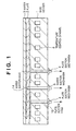
- Fig. 1 is a cross sectional view showing the structure of a substrate holding device (wafer chuck) of a semiconductor manufacturing apparatus according to a first embodiment of the present invention.
- Fig. 2 is an exploded perspective view showing respective parts of the substrate holding device in Fig. 1.
- the substrate holding device of the present embodiment is held on a drive mechanism called a wafer stage to sequentially transfer a circuit pattern on a reticle onto a semiconductor substrate (wafer).
- the wafer stage is capable of positioning in XYZ translation directions and XYZ axial rotation directions by a drive mechanism. Note that other functions than the substrate holding device are omitted.
- Numeral 1 denotes a base member fixed on the wafer stage (not shown).
- the base member 1 has a temperature control channel 6 to maintain a constant temperature of the member, and a temperature control medium is circulated through the channel. Note that in a case where the temperature of the substrate holding base is increased by heat upon exposure or heat from the drive mechanism, a coolant is used. Further, as the temperature control medium, pure water, oil or the like is used.
- Numeral 2 denotes a plate held on the base member 1, for directly holding a wafer 3. Upon chuck cleaning, only the plate 2 is removed and is cleaned. This operation will be described in detail later.
- the plate 2 is vacuum-sacked on the base member 1 by negative pressure in a gap between the base member 1 and the plate 2 caused by a plate suction mechanism 4.
- the base member 1 has a plate suction hole 15.
- Numeral 5 denotes a wafer suction mechanism to vacuum-suck the wafer on the plate 2.
- the wafer suction mechanism 5 is provided on the base member 1. Note that as a piping from the wafer suction mechanism 5 to the wafer, a wafer suction hole 14 is formed through the base member 1 and the plate 2 for holding the wafer 3 on the plate 2 by vacuum suction. That is, the plate 2 is placed on the base member 1 while the plate is aligned with the base member such that the suction hole provided in the plate 2 and the suction hole provided in the base member 1 are aligned with each other.
- the plate suction mechanism 4 and the wafer suction mechanism 5 function independently of each other.
- the vacuum suction mechanism is used for holding the wafer 3 and the plate 2, however, the present invention is not limited to the vacuum suction mechanism but any other holding mechanism such as an electrostatic chuck or a mechanical chuck can be used to obtain a similar advantage.
- the electrostatic chuck to hold the wafer 3
- the plate 2 is placed on the base member 1 while the plate is aligned with the base member such that an electrode provided in the plate 2 and an electrode provided in the base member 1 are aligned with each other.
- Numeral 7 denotes wafer contact pins for holding the wafer 3 on the plate 2.
- numeral 2a denotes a ring-shaped contact member provided on a rim of the plate 2.
- the wafer 3 is supported by the contact member 2a and the pins 7, and is flat-corrected.
- Numeral 8 denotes plate contact pins as contact members for holding the plate 2 on the base member 1.
- Numeral la denotes a ring-shaped contact member provided on a rim of the base member 1.
- the plate 2 is supported by the contact member la and the pins 8.
- the pin-shaped projections are used as the respective contact members.
- the contact members are not limited to the pin-shaped projections but any other members such as ring-shaped projections may be used as long as they attain a similar advantage. Further, even if the projections on the plate are pin-shaped projections, ring-shaped projections may be used on the base member.
- Fig. 3A shows the positional relation between the pins 7 provided on the plate 2 and the pins 8 provided on the base member 1.
- Fig. 3B shows a positional shift amount d between the central axis of the projection on the plate 2 (e.g. pin 7) and that of the projection on the base member 1 (e.g. pin 8).
- the plate 2 has a characteristic as an elastic body. Accordingly, when negative pressure occurs between the base member 1 and the plate 2 or between the plate 2 and the wafer 3, for example, the plate 2 is elastically deformed. However, even when the plate 2 is elastically deformed, the flatness of the surface of the pins 7 holding the wafer 3 must be maintained so as to flat-correct the wafer 3.
- the projections on the base member 1 are provided under the projections of the plate 2 (e.g. pins 7) as shown in Fig. 3A.
- the projections on the plate 2 and those on the base member 1 are coaxially arranged as much as possible.
- coaxial does not mean complete coaxial positioning but positioning such that the degradation of flatness caused in the plate 2 due to the positional shift d is within an allowable range. For example, if the positional shift d is equal to or less than 5 mm, the projections are coaxially positioned, and if the positional shift d is equal to or less than 1 mm, the projections are more preferably coaxially positioned, and further, if the positional shift d is equal to or less than 0.5 mm, the projections are further preferably coaxially positioned.
- the projections are in the "coaxial” relation. Further, it may be arranged such that the projections are in the "coaxial” relation if the central axis of the projection on the plate 2 is within the area of the projection of the base member 1.
- the projections on the base member 1 are arranged under all the projections on the plate 2. Note that the projections are not necessarily arranged in this manner. It is preferable that the projections on the base member 1 are provided under 90% of the projections on the plate 2.
- Numeral 13 denotes the wafer stage which is not shown in Figs. 1 and 2.
- the wafer stage 13 is capable of positioning in the XYZ translation directions and the XYZ axial rotation directions by a wafer stage drive mechanism 22.
- a bar mirror 11 as well as the above-described wafer chuck is mounted on the wafer stage 13.
- the bar mirror 11 is irradiated with a laser beam (interferometer beam) 12, thereby the position of the reflection surface of the bar mirror 11 is measured. That is, the position of the wafer stage 13 is measured by a laser interferometer (not shown) and the bar mirror 11.
- the result of measurement is inputted into a controller 21.
- the controller 21 outputs a drive signal to the wafer stage drive mechanism 22 based on the input position information of the wafer stage 13.
- the drive mechanism 22 drives the wafer stage 13 based on the drive signal.
- Numeral 9 denotes a hand for conveyance used for providing/collecting the wafer 3 and for providing/collecting the plate 2.
- the hand 9 grasps a side surface of the wafer 3 or the plate 2 by a grasp mechanism 10 included in the end of the hand 9.
- the grasp mechanism 10 is controlled based on a signal from the controller 21.
- a Z drive mechanism 25 drives the hand 9 in the Z direction.
- the Z drive mechanism 25 is controlled based on a signal from the controller 21.
- the wafer or plate grasped by the hand 9 can be placed on the base member or the like, or the placed wafer or plate can be removed. In the present embodiment, an edge portion of the wafer 3 and that of the plate 2 is grasped.
- pickup/placement upon conveyance is not limited to the grasp of the side surface.
- it may be arranged such that the wafer 3 is lifted in the Z direction from the plate 2 or the plate 2 is lifted in the Z direction from the base member 1, and the hand holds the bottom surface of the wafer 3 or the plate 2.
- a hand drive mechanism 23 is provided to drive the hand 9 in the Z or Y direction to, e.g., convey the wafer 3 and the plate 2 to the outside of the exposure chamber.
- the drive mechanism 23 drives the hand 9 based on a signal from the controller 21.
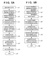
- Fig. 5A shows a sequence upon attachment of the plate 2 in the above construction
- Fig. 5B shows a sequence upon removal of the plate.
- the controller 21 controls necessary drive mechanisms and the like based on the sequences.
- a plate to be attached is designated from plural plates (a1).
- the designation of the plate is made e.g. by inputting a signal into the controller 21 or based on stored exposure information.
- the checking operation is made based on, e.g., signals from pressure sensors provided in the plate suction mechanism 4 and the wafer suction mechanism 5.
- the designated plate is conveyed from a plate carrier (not shown)(also usable as a wafer carrier) to the status as shown in Fig. 4 (a4).
- the plate suction mechanism 4 is changed to a sucking status, to suck-hold the plate 2 and the base member 1 (a6).
- the suction between the base member 1 and the plate 2 is made by vacuum suction here.
- the hand 9 changes the grasp mechanism 10 to a non-sucking status (a7), to withdraw the hand 9 (a8).
- the placement of the plate is completed (a9).
- the conveyance hand 9 is moved to hold the plate side surface (b3), and the grasp mechanism 10 of the conveyance hand 9 is changed to a grasping status (b4).
- the plate suction mechanism is released to change the plate into unsucked status (b5), and the hand 9 is moved upward by the Z drive mechanism 25, to separate the plate 2 from the base member 1 (b6), into the status as shown in Fig. 4. Thereafter, the plate 2 is conveyed onto the plate carrier (not shown).
- the plate 2 is previously processed so as to have a ultra-flat surface when placed on the base member 1. If there is a probability that dust is held between the plate and the base member upon attachment/removal, it is more preferable to provide a function or mechanism to check the flatness after the attachment/removal of the plate.
- the base member 1 and the plate 2 respectively have a ultra-flat surfaces.
- precision is obtained by grinding or lapping.
- a thin plate as in the present embodiment is distorted. Note that regarding thickness unevenness, such problem does not occur, therefore, high-precision thickness control can be made.
- the base member 1 has a ultra-flat surface, and the thickness of the plate 2 is controlled, such that the base member 1 flatten-corrects the plate 2. Accordingly, even if the plate 2 itself has slight distortion, the wafer-contact surface of the plate 2 can be corrected to be flat by sucking the plate 2 to the base member 1. For example, if the surfaces of both members are vacuum-sucked to each other in an area of ⁇ 300 mm (the area of sucked surfaces is about 707 cm 2 ), the suction can be made by a force of 707 kgf at the maximum, and this force can be utilized for correcting the distortion of the plate.
- the base member 1 receives a force to distort the base member.
- the base member is distorted by an amount exceeding the allowable range, the function to correct the flat surface of the wafer is finally degraded.
- the rigidity of the base member 1 is greater than that of the plate 2.
- the rigidity of the plate 2 is "1”
- the rigidity of the base member 1 is desirably "2" or greater.
- the relation of rigidity between the plate 2 and the base member 1 is the ratio of rigidity required of the base member 1 in this case (here the surface shape of the base member 1 is ignored for the sake of simple explanation). Note that the relation between the process precision and the ratio of rigidity (rigidity of plate 2/rigidity of base member 1) and the flatness of the plate 2 after flattening-correction is as follows.
- the contact surface of the plate 2 can be ultra flat by suck-holding the plate to the base member having sufficient rigidity.
- the flattening-correction can be made by increasing the rigidity of the base member with respect to the plate rigidity. Further, if the base member has rigidity higher than that of the plate, the flatness of the flatten-corrected plate 2 can be increased. Desirably, assuming that the rigidity of the plate 2 is "1", the rigidity of the base member 1 is "10" or greater. More desirably, assuming that the rigidity of the plate 2 is "1", the rigidity of the base member 1 is "20" or greater.
- the plate 2 is removed from the base member in accordance with a predetermined sequence.
- 1 ⁇ when contamination of the plate is detected and the contamination level is higher than a predetermined reference level the plate is removed to be exchanged with another plate; 2 ⁇ when a predetermined period has elapsed since the plate was set on the base member, the plate is removed to be exchanged with another plate; or 3 ⁇ when the substrate holding device is applied to an aligner, the plate is removed in accordance with an exposure history.
- Foreign materials attached to the plate 2 are removed by a cleaner (not shown), and the plate 2 is reused. Further, it is desirable to provide a device to detect foreign materials attached to the plate to be utilized, and it is further desirable to provide a device to detect smoothness, flaws and the like of the plate.
- an alignment reference mark 19 such as a notch or orientation/flat aligner is formed in the plate such that alignment is made upon conveyance of the plate as in the case of wafer.
- the alignment between the plate 2 and the base member 1 is not limited to this method, but any other alignment reference mark may be provided.
- an alignment mark may be formed on the plate 2, or a target for magnetic detection may be provided to detect the relative position of the plate 2 to the base member, or the plate 2 may have an edge so as to be measured from the base member 1. In this case, it is desirable to provide a sensor to detect the alignment reference mark.
- the sensor may be provided on the base member 1.
- plates used in exposure are managed by barcode or inscription.
- management is not only made by barcode or inscription but may be made by any sign for identifying the plate.
- the plate 2 is desirably made of a ceramic (e.g., SiC, SiN) material.
- the substrate holding base member to hold the plate 2 is desirably made of ceramic material.
- a cooling mechanism included in the base member 1 performs temperature control in a short period. Note that to effectively control the temperature of the plate 2 by the base member 1, thermal transfer from the base member 1 to the plate 2 can be increased by filling gas in the space sucking the both members to each other. That is, the pressure of the gap between the base member 1 and the plate 2 is controlled to an extent to which the plate 2 can be sucked, so as not to attain a vacuum state where almost no gas exists in the gap.
- the plate suction mechanism 4 desirably has a pressure regulating mechanism (not shown) and a pressure sensor (not shown).
- the controller 21 inputs a signal regarding the pressure outputted from the pressure sensor, and controls the pressure regulating mechanism based on the pressure signal.
- a throttle or the like can be used as the pressure regulating mechanism. The pressure can be controlled by controlling the opening area of the throttle.
- the wafer is conveyed by a conveyance device (not shown) from the wafer carrier (not shown) in a similar manner to that of the conveyance of the plate 2.
- the wafer 3 is conveyed to a position above the plate 2, then the wafer is moved downward by the Z drive mechanism 25, into contact with the plate 2.
- the both members are suck-held by changing the wafer suction mechanism 5 in Fig. 1 to a sucking status.
- the wafer and the plate is suck-held by vacuum suction.
- the grasp mechanism 10 in the hand 9 is changed to a non-grasping status, and the hand 9 withdraws, thus plate placement is completed. Further, when the wafer is removed, the above operation is made in the reversed order.
- the plate 2 and the wafer 3 are conveyed by the same conveyance device, however, they may be conveyed by different conveyance devices depending on system.
- the plate which may be contaminated due to attachment of photosensitive material or the like upon contact with wafer, can be replaced with another plate. Accordingly, in comparison with the conventional art, time to remove the contaminants is not required, and the productivity can be improved.
- Fig. 6 is a cross sectional view showing the structure of the substrate holding device (wafer chuck) of the semiconductor manufacturing apparatus according to a second embodiment of the present invention.
- the second embodiment uses a plate 32 corresponding to the wafer diameter.
- wafers having different diameters such as a ⁇ 300 mm (12 inch) wafer and a ⁇ 200 mm (8 inch) wafer are exposed by a single apparatus
- a wafer chuck for the ⁇ 300 mm wafer must be exchanged with a wafer chuck for the ⁇ 200 mm wafer.
- wafers having various diameters can be handled only by changing the plate shape to have a convexity as shown in Fig 6. That is, in the present embodiment, the area of the plate to suck-hold the wafer can be changed by appropriately changing the plate.
- the type of wafer to be held is specified from an exposure condition inputted into the controller 21 or stored in the memory (not shown) of the controller 21. Then the controller 21 designates a plate to be sucked on the base member 1 based on the specified wafer type.
- the identification of the plate at this time may be made by using an identification sign such as a barcode provided on the plate. Note that attachment/removal of the plate thereafter is made in the same manner as that described in the first embodiment.
- vacuum suction is used as an attraction mechanism of the base member 1 and the plate 2 (34) in the above first and second embodiments, other mechanisms such as electrostatic attraction, magnetic attraction and mechanical fixing may be used.
- a mirror platen 96 is supported by a floor or base 91 via a damper 98. Further, the mirror platen 96 supports a reticle stage platen 94 and supports a projection optical system 97 positioned between a reticle stage 95 and a wafer stage 93.
- the wafer stage 93 supported on a stage platen 92 supported by the floor or base 91, for carrying and positioning the wafer.
- the reticle stage 95 supported on the reticle stage platen 94 supported by the mirror platen 96, is movable while carrying a reticle having a circuit pattern. Exposure light to expose the reticle mounted on the reticle stage 95 is emitted from an illumination optical system 99.
- the wafer stage 93 is scanned in synchronization with the reticle stage 95. While the reticle stage 95 and the wafer stage 93 are scanned, the positions of these stages are continuously detected respectively by interferometers, and fed back to driving units of the reticle stage 95 and the wafer stage 93. This attains accurate synchronization between the scan start positions of these stages and high-precision control on scanning speed in a constant-speed scan area. While these stages are scanned with respect to the projection optical system 97, the reticle pattern is exposed and thus the circuit pattern is transferred onto the wafer.
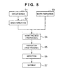
- Fig. 8 shows a flow of fabrication of semiconductor device (semiconductor chip such as an IC or an LSI or a liquid crystal panel, a CCD or the like).
- semiconductor device semiconductor chip such as an IC or an LSI or a liquid crystal panel, a CCD or the like.
- a circuit design of the semiconductor device is made.
- mask fabrication a mask where the designed circuit pattern is formed is fabricated.
- wafer fabrication a wafer is fabricated by using material such as silicon.
- preprocess the mask and the wafer are used for forming an actual circuit on the wafer by lithography.
- step S5 fabrication
- step S4 the wafer fabricated at step S4 is used for forming a semiconductor chip.
- the step S5 includes an assembly process (dicing and bonding), a packaging process (chip encapsulation) and the like.
- step S6 inspections such as an operation test and an endurance test are performed on the semiconductor device fabricated at step 5. Through these processes, the semiconductor device is completed and shipped (step S7).
- Fig. 9 shows the wafer process in detail.
- step S11 oxidation
- step S12 CVD
- step S13 electrode formation
- step S14 ion implantation
- ions are implanted into the wafer.
- step S15 resist processing
- step S16 exposure
- step S18 etching
- step S19 resist stripping
- the substrate holding device of the present invention as the plate can be removed and cleaned, time to remove contaminants is not required. Thus the productivity can be improved. Further, as the plate on the flat plate can be removed, cleaning to remove the contaminants can be easily performed.
Landscapes
- Physics & Mathematics (AREA)
- General Physics & Mathematics (AREA)
- Engineering & Computer Science (AREA)
- Public Health (AREA)
- Health & Medical Sciences (AREA)
- Epidemiology (AREA)
- Atmospheric Sciences (AREA)
- Life Sciences & Earth Sciences (AREA)
- Plasma & Fusion (AREA)
- Environmental & Geological Engineering (AREA)
- Container, Conveyance, Adherence, Positioning, Of Wafer (AREA)
- Exposure And Positioning Against Photoresist Photosensitive Materials (AREA)
- Exposure Of Semiconductors, Excluding Electron Or Ion Beam Exposure (AREA)
Abstract
Description
Claims (62)
- A substrate holding device characterized by comprising:a base member capable of removably holding a plate having a contact member to come into contact with a substrate;a first attraction mechanism that attracts said substrate onto said plate in a status where said plate is held on said base member; anda second attraction mechanism that attracts said plate onto said base member.
- The substrate holding device according to claim 1, characterized in that said first attraction mechanism performs any of vacuum suction, electrostatic attraction, magnetic attraction or mechanical fixing.
- The substrate holding device according to claim 1, characterized in that said second attraction mechanism performs any of vacuum suction, electrostatic attraction or mechanical fixing.
- The substrate holding device according to claim 1, characterized in that said base member has a pin or ring to come into contact with said plate.
- The substrate holding device according to claim 4,
characterized in that said pin or ring is provided in a position approximately the same as that of a pin or ring provided on said plate. - The substrate holding device according to claim 1, characterized in that said base member is provided on a movable stage.
- The substrate holding device according to claim 1, characterized in that said first attraction mechanism and said second attraction mechanism operate independently of each other.
- The substrate holding device according to claim 1, characterized in that said plate is removed from said base member in accordance with a predetermined sequence.
- The substrate holding device according to claim 8, characterized in that said plate is removed from said base member when said plate is contaminated.
- The substrate holding device according to claim 8, characterized in that said plate is removed from said base member when a predetermined period has elapsed.
- The substrate holding device according to claim 8, characterized in that said plate is removed from said base member in accordance with an exposure history.
- The substrate holding device according to claim 1, characterized in that a sign for identification of said plate is provided on said plate.
- The substrate holding device according to claim 12, characterized in that a barcode or inscription is provided on said plate.
- The substrate holding device according to claim 1, characterized in that said base member comprises a ceramic material.
- The substrate holding device according to claim 1, characterized in that said plate comprises a ceramic material.
- The substrate holding device according to claim 1, further characterized by comprising a temperature control mechanism for controlling a temperature of said base member.
- The substrate holding device according to claim 16, characterized in that said base member has a temperature control channel through which a temperature control medium flows.
- A substrate holding device characterized by comprising:a base member capable of removably holding a plate having a contact member to come into contact with a substrate,wherein said base member flatten-corrects said plate by sucking said plate.
- The substrate holding device according to claim 18, characterized in that rigidity of said base member is higher than that of said plate.
- The substrate holding device according to claim 18, characterized in that said base member comprises a ceramic material.
- The substrate holding device according to claim 18, characterized in that said base member has a temperature control mechanism that controls a temperature of said plate.
- The substrate holding device according to claim 18, characterized in that a projection is provided on said base member, and the projection is coaxial with a projection provided on said plate.
- A substrate holding device characterized by comprising:a base member capable of removably holding a plate having a contact member to come into contact with a substrate,wherein rigidity of said base member is higher than that of said plate.
- The substrate holding device according to claim 23, characterized in that assuming that the rigidity of said substrate is 1, the rigidity of said base member is 2 or greater.
- The substrate holding device according to claim 24, characterized in that assuming that the rigidity of said substrate is 1, the rigidity of said base member is 10 or greater.
- The substrate holding device according to claim 24, characterized in that assuming that the rigidity of said substrate is 1, the rigidity of said base member is 20 or greater.
- A substrate holding device characterized by comprising:a base member capable of removably holding a plate having a projection to come into contact with a substrate; anda projection, provided on said base member, that holds said plate,wherein said projection is provided on said base member so as to be positioned under the projection provided on said plate.
- The substrate holding device according to claim 27, characterized in that said projection provided on said base member has a pin or ring shape.
- The substrate holding device according to claim 27, characterized in that said projection provided on said base member is provided under 90% or more of projections provided on said plate.
- The substrate holding device according to claim 27, characterized in that a reference mark for alignment is provided on said plate.
- The substrate holding device according to claim 30, characterized in that said reference mark is at least any of an orientation/flat aligner, an alignment mark, a magnetic target and an edge.
- A substrate holding device characterized by comprising:a base member capable of removably holding a plate having a projection to come into contact with a substrate; anda projection, provided on said base member, that holds said plate,wherein said projection and the projection provided on said plate are coaxially provided.
- A substrate holding device characterized by comprising:a base member capable of removably holding a plate having a projection to come into contact with a substrate; anda projection, provided on said base member, that holds said plate,wherein a central axis of the projection provided on said plate is positioned within an area of said projection provided on said base member.
- A substrate holding device characterized by comprising:a base member capable of removably holding a plate having a projection to come into contact with a substrate; anda projection, provided on said base member, that holds said plate,wherein a central axis of said projection provided on said base member is positioned within a range of 5 mm from a center of the projection provided on said plate.
- The substrate holding device according to claim 34, characterized in that the amount of shift between the central axis of said projection on said base member and the projection on said plate is equal to or less than 1 mm.
- The substrate holding device according to claim 35, characterized in that the amount of shift between the central axis of said projection on said base member and the projection on said plate is equal to or less than 0.5 mm.
- A substrate holding device characterized by comprising:a base member capable of removably holding a plate having a contact member to come into contact with a substrate; anda pressure control mechanism that controls pressure in a gap between said base member and said plate.
- The substrate holding device according to claim 37, characterized in that said pressure control mechanism controls the pressure such that gas remains in said gap.
- The substrate holding device according to claim 37, characterized in that said pressure control mechanism has a throttle.
- The substrate holding device according to claim 37, characterized in that said pressure control mechanism has a sensor that detects the pressure.
- A substrate holding device characterized by comprising:a base member capable of removably holding a plate having a contact member to come into contact with a substrate; anda sensor that identifies an identification sign provided on said plate.
- The substrate holding device according to claim 41, further characterized by comprising a storage device in that a status of use of said plate is stored based on an identification signal from said sensor.
- The substrate holding device according to claim 41, further characterized by comprising a controller that selects said plate based on an identification signal from said sensor.
- The substrate holding device according to claim 43, characterized in that said controller selects said plate based on information on type of said substrate.
- The substrate holding device according to claim 44, characterized in that the information on type of said substrate is outputted based on a signal indicative of exposure condition.
- A semiconductor manufacturing apparatus characterized by comprising:a base member capable of removably holding a plate having a contact member to come into contact with a substrate;a first attraction mechanism that attracts said substrate onto said plate in a status where said plate is held on said base member; anda second attraction mechanism that attracts said plate onto said base member.
- The semiconductor manufacturing apparatus according to claim 46, further characterized by comprising a conveyance mechanism that conveys said plate.
- The semiconductor manufacturing apparatus according to claim 47, characterized in that said conveyance mechanism holds a side surface of said plate.
- The semiconductor manufacturing apparatus according to claim 47, characterized in that said conveyance mechanism conveys a plate designated from prepared plates.
- The semiconductor manufacturing apparatus according to claim 47, characterized in that said plate, removed by said conveyance mechanism, is cleaned, and said plate is conveyed to said base member by said conveyance mechanism.
- The semiconductor manufacturing apparatus according to claim 47, further characterized by comprising a storage device in that a status of use of said plate is stored.
- A semiconductor manufacturing apparatus characterized by comprising:a base member capable of removably holding a plate having a contact member to come into contact with a substrate,wherein said base member flatten-corrects said plate by sucking said plate.
- A semiconductor manufacturing apparatus characterized by comprising:a base member capable of removably holding a plate having a contact member to come into contact with a substrate,wherein rigidity of said base member is higher than that of said plate.
- A semiconductor manufacturing apparatus characterized by comprising:a base member capable of removably holding a plate having a projection to come into contact with a substrate; anda projection, provided on said base member, that holds said plate,wherein said projection is provided on said base member so as to be positioned under the projection provided on said plate.
- The semiconductor manufacturing apparatus characterized by comprising:a base member capable of removably holding a plate having a projection to come into contact with a substrate; anda projection, provided on said base member, that holds said plate,wherein said projection and the projection provided on said plate are coaxially provided.
- The semiconductor manufacturing apparatus characterized by comprising:a base member capable of removably holding a plate having a projection to come into contact with a substrate; anda projection, provided on said base member, that holds said plate,wherein a central axis of the projection provided on said plate is positioned within an area of said projection provided on said base member.
- The semiconductor manufacturing apparatus characterized by comprising:a base member capable of removably holding a plate having a projection to come into contact with a substrate; anda projection, provided on said base member, that holds said plate,wherein a central axis of said projection provided on said base member is positioned within a range of 5 mm from a center of the projection provided on said plate.
- The semiconductor manufacturing apparatus characterized by comprising:a base member capable of removably holding a plate having a contact member to come into contact with a substrate; anda pressure control mechanism that controls pressure in a gap between said base member and said plate.
- The semiconductor manufacturing apparatus characterized by comprising:a base member capable of removably holding a plate having a contact member to come into contact with a substrate; anda sensor that identifies an identification sign provided on said plate.
- A device manufacturing method characterized by comprising:a step of applying photosensitive agent to a substrate;a step of preparing the semiconductor manufacturing apparatus in claims 46, 52 to 59;a step of exposing a master pattern on said substrate;a step of developing said substrate exposed at said exposing step; anda step of manufacturing a device from the exposed and developed substrate.
- A method of mounting a substrate to a substrate holding device, comprising the steps of:providing a plate having a contact member for contacting the substrate;attracting, with an attraction means, said plate to a base of said holding device;attracting, with a second attraction means, said substrate to said plate so that said contact member of said plate contacts said substrate.
- A method of exposing a substrate to a pattern, comprising mounting said substrate to a substrate holding device by the method of claim 61, and exposing the mounted substrate to said pattern.
Priority Applications (2)
| Application Number | Priority Date | Filing Date | Title |
|---|---|---|---|
| EP10151068A EP2192608A1 (en) | 2000-03-10 | 2001-03-09 | Substrate holding device |
| EP07075481A EP1843382B1 (en) | 2000-03-10 | 2001-03-09 | Substrate holding device |
Applications Claiming Priority (4)
| Application Number | Priority Date | Filing Date | Title |
|---|---|---|---|
| JP2000066378 | 2000-03-10 | ||
| JP2000066378 | 2000-03-10 | ||
| JP2001040169A JP4700819B2 (en) | 2000-03-10 | 2001-02-16 | Substrate holding apparatus, semiconductor manufacturing apparatus, and semiconductor device manufacturing method |
| JP2001040169 | 2001-02-16 |
Related Child Applications (1)
| Application Number | Title | Priority Date | Filing Date |
|---|---|---|---|
| EP07075481A Division EP1843382B1 (en) | 2000-03-10 | 2001-03-09 | Substrate holding device |
Publications (3)
| Publication Number | Publication Date |
|---|---|
| EP1132948A2 true EP1132948A2 (en) | 2001-09-12 |
| EP1132948A3 EP1132948A3 (en) | 2006-04-26 |
| EP1132948B1 EP1132948B1 (en) | 2008-10-15 |
Family
ID=26587170
Family Applications (3)
| Application Number | Title | Priority Date | Filing Date |
|---|---|---|---|
| EP01302152A Expired - Lifetime EP1132948B1 (en) | 2000-03-10 | 2001-03-09 | Substrate holding device and method of mounting a substrate to a substrate holding device |
| EP10151068A Withdrawn EP2192608A1 (en) | 2000-03-10 | 2001-03-09 | Substrate holding device |
| EP07075481A Expired - Lifetime EP1843382B1 (en) | 2000-03-10 | 2001-03-09 | Substrate holding device |
Family Applications After (2)
| Application Number | Title | Priority Date | Filing Date |
|---|---|---|---|
| EP10151068A Withdrawn EP2192608A1 (en) | 2000-03-10 | 2001-03-09 | Substrate holding device |
| EP07075481A Expired - Lifetime EP1843382B1 (en) | 2000-03-10 | 2001-03-09 | Substrate holding device |
Country Status (4)
| Country | Link |
|---|---|
| US (3) | US6862080B2 (en) |
| EP (3) | EP1132948B1 (en) |
| JP (1) | JP4700819B2 (en) |
| DE (2) | DE60142862D1 (en) |
Cited By (7)
| Publication number | Priority date | Publication date | Assignee | Title |
|---|---|---|---|---|
| WO2002095806A1 (en) * | 2001-05-18 | 2002-11-28 | Tokyo Electron Limited | Universal backplane assembly and methods |
| WO2005009089A3 (en) * | 2003-07-23 | 2005-09-01 | Matsushita Electric Industrial Co Ltd | Plasma processing apparatus |
| WO2006025341A1 (en) | 2004-09-01 | 2006-03-09 | Nikon Corporation | Substrate holder, stage apparatus, and exposure apparatus |
| WO2006069942A1 (en) * | 2004-12-27 | 2006-07-06 | Alphasem Ag | Device for fixing a flat object, in particular a substrate, to a work surface by means of low pressure |
| ITUD20110079A1 (en) * | 2011-06-06 | 2012-12-07 | Applied Materials Italia Srl | SUPPORT AND TRANSPORT UNIT FOR A PRINTING SUBSTRATE FOR A PRINT TRACK DEPOSITION PLANT, AND ITS DEPOSITION PROCEDURE |
| CN110957256A (en) * | 2018-09-27 | 2020-04-03 | 东京毅力科创株式会社 | Substrate processing equipment |
| US20210033523A1 (en) * | 2001-06-29 | 2021-02-04 | Meso Scale Technologies, Llc. | Assay plates, reader systems and methods for luminescence test measurements |
Families Citing this family (50)
| Publication number | Priority date | Publication date | Assignee | Title |
|---|---|---|---|---|
| JP4700819B2 (en) * | 2000-03-10 | 2011-06-15 | キヤノン株式会社 | Substrate holding apparatus, semiconductor manufacturing apparatus, and semiconductor device manufacturing method |
| JP2003158173A (en) * | 2001-11-20 | 2003-05-30 | Oki Electric Ind Co Ltd | Wafer holder |
| AU2003236002A1 (en) * | 2002-04-11 | 2003-10-20 | Disco Corporation | Method for manufacturing semiconductor chip |
| JP2004103799A (en) * | 2002-09-09 | 2004-04-02 | Canon Inc | Substrate holding device, device manufacturing apparatus and device manufacturing method |
| CN1311301C (en) * | 2002-12-23 | 2007-04-18 | Asml荷兰有限公司 | Photoetching projection device |
| CN100383951C (en) * | 2003-07-23 | 2008-04-23 | 松下电器产业株式会社 | Plasma processing equipment |
| US7370659B2 (en) * | 2003-08-06 | 2008-05-13 | Micron Technology, Inc. | Photolithographic stepper and/or scanner machines including cleaning devices and methods of cleaning photolithographic stepper and/or scanner machines |
| TWI220451B (en) * | 2003-10-14 | 2004-08-21 | Ind Tech Res Inst | Positioning measurement platform of optoelectronic device |
| JP2005150527A (en) * | 2003-11-18 | 2005-06-09 | Canon Inc | Holding apparatus, exposure apparatus using the same, and device manufacturing method |
| SG186621A1 (en) * | 2004-06-09 | 2013-01-30 | Nikon Corp | Substrate holding device, exposure apparatus having same, exposure method, method for producing device, and liquid repellent plate |
| JP2005353988A (en) * | 2004-06-14 | 2005-12-22 | Canon Inc | Plate-like body conveying method, conveying apparatus and exposure apparatus |
| JP2006147776A (en) * | 2004-11-18 | 2006-06-08 | Nikon Corp | Maintenance apparatus, maintenance method, and exposure apparatus |
| US7583358B2 (en) * | 2005-07-25 | 2009-09-01 | Micron Technology, Inc. | Systems and methods for retrieving residual liquid during immersion lens photolithography |
| US7456928B2 (en) * | 2005-08-29 | 2008-11-25 | Micron Technology, Inc. | Systems and methods for controlling ambient pressure during processing of microfeature workpieces, including during immersion lithography |
| EP1780764A1 (en) * | 2005-11-01 | 2007-05-02 | FEI Company | Stage assembly, particle-optical apparatus comprising such a stage assembly, and method of treating a sample in such an apparatus |
| US8472004B2 (en) * | 2006-01-18 | 2013-06-25 | Micron Technology, Inc. | Immersion photolithography scanner |
| US20070217119A1 (en) * | 2006-03-17 | 2007-09-20 | David Johnson | Apparatus and Method for Carrying Substrates |
| JP2007281053A (en) * | 2006-04-04 | 2007-10-25 | Miraial Kk | Thin plate storage container |
| WO2007114331A1 (en) * | 2006-04-04 | 2007-10-11 | Miraial Co., Ltd. | Thin plate container |
| US7978308B2 (en) * | 2006-05-15 | 2011-07-12 | Asml Netherlands B.V. | Lithographic apparatus and device manufacturing method |
| US8760621B2 (en) * | 2007-03-12 | 2014-06-24 | Asml Netherlands B.V. | Lithographic apparatus and method |
| GB2449213B (en) | 2007-05-18 | 2011-06-29 | Kraft Foods R & D Inc | Improvements in or relating to beverage preparation machines and beverage cartridges |
| JP2010084207A (en) * | 2008-09-30 | 2010-04-15 | Canon Anelva Corp | Processing apparatus and image display device |
| JP2010084205A (en) * | 2008-09-30 | 2010-04-15 | Canon Anelva Corp | Holding mechanism, processing apparatus with the holding mechanism, deposition method using processing apparatus, and method of manufacturing image display device |
| NL2003528A (en) * | 2008-10-23 | 2010-04-26 | Asml Netherlands Bv | Lithographic apparatus and device manufacturing method. |
| NL2003845A (en) * | 2008-12-19 | 2010-06-22 | Asml Netherlands Bv | Lithographic apparatus, and patterning device for use in a lithographic process. |
| JP5345161B2 (en) * | 2011-01-20 | 2013-11-20 | 東京エレクトロン株式会社 | Wafer carrier for power device and inspection apparatus using this wafer carrier |
| CN109254501A (en) | 2012-02-03 | 2019-01-22 | Asml荷兰有限公司 | Substrate holder, lithographic apparatus, device manufacturing method, and method of manufacturing a substrate holder |
| CN103531511B (en) * | 2012-07-04 | 2017-02-08 | 上海微电子装备有限公司 | Sucking disc, wafer bearing stage using same and wafer adsorption method |
| JP6076043B2 (en) * | 2012-11-02 | 2017-02-08 | 株式会社ディスコ | Chuck table |
| JP5575934B2 (en) * | 2013-01-25 | 2014-08-20 | 東京エレクトロン株式会社 | Joining apparatus and joining system |
| DE112014001440T5 (en) * | 2013-03-15 | 2016-01-14 | Rudolph Technologies, Inc. | Flexible handling system for semiconductor substrates |
| US9698070B2 (en) * | 2013-04-11 | 2017-07-04 | Infineon Technologies Ag | Arrangement having a plurality of chips and a chip carrier, and a processing arrangement |
| CN103325722B (en) * | 2013-05-24 | 2016-04-20 | 沈阳拓荆科技有限公司 | Wafer conveying mechanism and using method |
| JP6189646B2 (en) * | 2013-05-30 | 2017-08-30 | 東レエンジニアリング株式会社 | Transport device |
| CN104637854B (en) * | 2013-11-13 | 2018-12-07 | 沈阳新松机器人自动化股份有限公司 | It is a kind of for adsorbing the sucker of silicon wafer |
| JP6498550B2 (en) * | 2015-07-14 | 2019-04-10 | 株式会社ディスコ | Turning device |
| JP6833350B2 (en) * | 2016-06-01 | 2021-02-24 | キヤノン株式会社 | Manufacturing methods for holding devices, transport devices, lithography equipment, and articles |
| KR102008515B1 (en) * | 2017-03-13 | 2019-10-22 | 한미반도체 주식회사 | semiconductor manufacturing apparatus and controlling method of the same |
| JP2019075477A (en) * | 2017-10-17 | 2019-05-16 | 株式会社ディスコ | Chuck table mechanism |
| KR102456532B1 (en) * | 2017-11-20 | 2022-10-18 | 에이에스엠엘 네델란즈 비.브이. | A substrate holder, a substrate support, and a method for clamping a substrate to a clamping system |
| JP2019115962A (en) * | 2017-12-27 | 2019-07-18 | 株式会社ディスコ | Chuck table correction method, and cutting device |
| JP7210896B2 (en) * | 2018-04-23 | 2023-01-24 | 東京エレクトロン株式会社 | SUBSTRATE PLACEMENT DEVICE AND SUBSTRATE PLACEMENT METHOD |
| JP7110053B2 (en) * | 2018-09-27 | 2022-08-01 | 東京エレクトロン株式会社 | Substrate processing equipment |
| WO2021201108A1 (en) * | 2020-03-31 | 2021-10-07 | 京セラ株式会社 | Flow path member and method for manufacturing same |
| US11794314B2 (en) * | 2021-08-30 | 2023-10-24 | Kla Corporation | Quick swap chuck with vacuum holding interchangeable top plate |
| KR102750081B1 (en) * | 2022-05-23 | 2025-01-03 | 세메스 주식회사 | Substrate processing apparatus |
| CN115632029B (en) * | 2022-12-22 | 2023-03-17 | 河北博特半导体设备科技有限公司 | Ceramic rotating platform structure of high-precision wafer bearing platform |
| JP2024104843A (en) * | 2023-01-25 | 2024-08-06 | 日本特殊陶業株式会社 | Retaining material |
| EP4632486A3 (en) * | 2025-08-29 | 2026-03-04 | ASML Netherlands B.V. | A conditioning unit for a substrate |
Family Cites Families (30)
| Publication number | Priority date | Publication date | Assignee | Title |
|---|---|---|---|---|
| US4278348A (en) * | 1979-11-26 | 1981-07-14 | Quintel Corporation | Locking mechanism for use in a chuck for an optical alignment and exposure apparatus |
| JPS6022319A (en) * | 1983-07-18 | 1985-02-04 | Canon Inc | Semiconductor exposure apparatus |
| US4755747A (en) * | 1984-06-15 | 1988-07-05 | Canon Kabushiki Kaisha | Wafer prober and a probe card to be used therewith |
| JP2649519B2 (en) * | 1987-07-21 | 1997-09-03 | キヤノン株式会社 | Flat object transfer positioning device |
| DE69032740T2 (en) * | 1989-12-20 | 1999-06-02 | Koninklijke Philips Electronics N.V., Eindhoven | Information coding method for chip identification using step litographic methods |
| JP2748181B2 (en) | 1990-07-26 | 1998-05-06 | キヤノン株式会社 | Wafer chuck |
| JPH04152512A (en) * | 1990-10-16 | 1992-05-26 | Fujitsu Ltd | Wafer chuck |
| DE69118315T2 (en) * | 1990-11-01 | 1996-08-14 | Canon Kk | Wafer holding fixture for exposure device |
| JPH0710493Y2 (en) | 1991-02-05 | 1995-03-08 | 株式会社エンヤシステム | Wafer pasting board |
| JP3168018B2 (en) * | 1991-03-22 | 2001-05-21 | キヤノン株式会社 | Substrate suction holding method |
| JP2919158B2 (en) * | 1992-02-10 | 1999-07-12 | キヤノン株式会社 | Substrate holding device |
| US5409348A (en) * | 1992-05-15 | 1995-04-25 | Tokyo Electron Limited | Substrate transfer method |
| JP3173928B2 (en) * | 1992-09-25 | 2001-06-04 | キヤノン株式会社 | Substrate holding apparatus, substrate holding method, and exposure apparatus |
| US5382311A (en) * | 1992-12-17 | 1995-01-17 | Tokyo Electron Limited | Stage having electrostatic chuck and plasma processing apparatus using same |
| JPH06196381A (en) * | 1992-12-22 | 1994-07-15 | Canon Inc | Substrate holding device |
| US5409384A (en) * | 1993-04-08 | 1995-04-25 | The Whitaker Corporation | Low profile board-to-board electrical connector |
| JPH07130637A (en) | 1993-10-29 | 1995-05-19 | Canon Inc | Semiconductor manufacturing equipment |
| JPH08257469A (en) * | 1995-01-24 | 1996-10-08 | Canon Inc | Substrate rotating device and substrate processing device |
| JPH09102453A (en) * | 1995-10-03 | 1997-04-15 | Nikon Corp | Substrate holding member and exposure apparatus |
| JPH09283609A (en) * | 1996-04-12 | 1997-10-31 | Nhk Spring Co Ltd | Electrostatic clamping device |
| JPH1076439A (en) * | 1996-08-30 | 1998-03-24 | Sony Corp | Thin plate holding device |
| JPH10116760A (en) * | 1996-10-08 | 1998-05-06 | Nikon Corp | Exposure device and substrate holding device |
| US5803797A (en) * | 1996-11-26 | 1998-09-08 | Micron Technology, Inc. | Method and apparatus to hold intergrated circuit chips onto a chuck and to simultaneously remove multiple intergrated circuit chips from a cutting chuck |
| JPH10233426A (en) * | 1997-02-20 | 1998-09-02 | Tokyo Electron Ltd | Automatic teaching method |
| JPH1165093A (en) | 1997-08-19 | 1999-03-05 | Canon Inc | Substrate management device, substrate storage container, substrate storage device, and device manufacturing method |
| JPH11121362A (en) * | 1997-10-20 | 1999-04-30 | Canon Inc | Exposure apparatus and device manufacturing method |
| US6073681A (en) * | 1997-12-31 | 2000-06-13 | Temptronic Corporation | Workpiece chuck |
| JPH11243127A (en) * | 1998-02-25 | 1999-09-07 | Jeol Ltd | Processing equipment |
| JP4700819B2 (en) * | 2000-03-10 | 2011-06-15 | キヤノン株式会社 | Substrate holding apparatus, semiconductor manufacturing apparatus, and semiconductor device manufacturing method |
| JP2002353099A (en) * | 2001-05-22 | 2002-12-06 | Canon Inc | Position detecting method and apparatus, exposure apparatus and device manufacturing method |
-
2001
- 2001-02-16 JP JP2001040169A patent/JP4700819B2/en not_active Expired - Fee Related
- 2001-03-06 US US09/799,060 patent/US6862080B2/en not_active Expired - Lifetime
- 2001-03-09 EP EP01302152A patent/EP1132948B1/en not_active Expired - Lifetime
- 2001-03-09 EP EP10151068A patent/EP2192608A1/en not_active Withdrawn
- 2001-03-09 DE DE60142862T patent/DE60142862D1/en not_active Expired - Lifetime
- 2001-03-09 DE DE60136119T patent/DE60136119D1/en not_active Expired - Lifetime
- 2001-03-09 EP EP07075481A patent/EP1843382B1/en not_active Expired - Lifetime
-
2004
- 2004-09-02 US US10/931,984 patent/US6982784B2/en not_active Expired - Fee Related
-
2005
- 2005-09-08 US US11/220,677 patent/US7102735B2/en not_active Expired - Fee Related
Cited By (11)
| Publication number | Priority date | Publication date | Assignee | Title |
|---|---|---|---|---|
| WO2002095806A1 (en) * | 2001-05-18 | 2002-11-28 | Tokyo Electron Limited | Universal backplane assembly and methods |
| US6645344B2 (en) | 2001-05-18 | 2003-11-11 | Tokyo Electron Limited | Universal backplane assembly and methods |
| US20210033523A1 (en) * | 2001-06-29 | 2021-02-04 | Meso Scale Technologies, Llc. | Assay plates, reader systems and methods for luminescence test measurements |
| WO2005009089A3 (en) * | 2003-07-23 | 2005-09-01 | Matsushita Electric Industrial Co Ltd | Plasma processing apparatus |
| US7708860B2 (en) | 2003-07-23 | 2010-05-04 | Panasonic Corporation | Plasma processing apparatus |
| WO2006025341A1 (en) | 2004-09-01 | 2006-03-09 | Nikon Corporation | Substrate holder, stage apparatus, and exposure apparatus |
| EP1796143A4 (en) * | 2004-09-01 | 2009-06-17 | Nikon Corp | SUBSTRATE CARRIER, PLATINUM APPARATUS, AND EXPOSURE APPARATUS |
| US8717543B2 (en) | 2004-09-01 | 2014-05-06 | Nikon Corporation | Substrate holder, stage apparatus, and exposure apparatus with first support part provided in a suction space and second support part |
| WO2006069942A1 (en) * | 2004-12-27 | 2006-07-06 | Alphasem Ag | Device for fixing a flat object, in particular a substrate, to a work surface by means of low pressure |
| ITUD20110079A1 (en) * | 2011-06-06 | 2012-12-07 | Applied Materials Italia Srl | SUPPORT AND TRANSPORT UNIT FOR A PRINTING SUBSTRATE FOR A PRINT TRACK DEPOSITION PLANT, AND ITS DEPOSITION PROCEDURE |
| CN110957256A (en) * | 2018-09-27 | 2020-04-03 | 东京毅力科创株式会社 | Substrate processing equipment |
Also Published As
| Publication number | Publication date |
|---|---|
| US6862080B2 (en) | 2005-03-01 |
| US20060033904A1 (en) | 2006-02-16 |
| EP1843382A3 (en) | 2008-01-02 |
| EP1843382A2 (en) | 2007-10-10 |
| EP2192608A1 (en) | 2010-06-02 |
| JP2001326270A (en) | 2001-11-22 |
| DE60142862D1 (en) | 2010-09-30 |
| EP1132948A3 (en) | 2006-04-26 |
| DE60136119D1 (en) | 2008-11-27 |
| US20010033369A1 (en) | 2001-10-25 |
| EP1843382B1 (en) | 2010-08-18 |
| JP4700819B2 (en) | 2011-06-15 |
| EP1132948B1 (en) | 2008-10-15 |
| US6982784B2 (en) | 2006-01-03 |
| US7102735B2 (en) | 2006-09-05 |
| US20050018169A1 (en) | 2005-01-27 |
Similar Documents
| Publication | Publication Date | Title |
|---|---|---|
| EP1132948B1 (en) | Substrate holding device and method of mounting a substrate to a substrate holding device | |
| US20020008864A1 (en) | Substrate holding apparatus and exposure apparatus including substrate holding apparatus | |
| JP3978140B2 (en) | Configuration and method for detecting defects on a substrate in a processing tool | |
| EP0947884A2 (en) | Lithographic projection apparatus with substrate holder | |
| JPH07153663A (en) | Mask holding method, mask and mask chuck, and exposure apparatus and device manufacturing method using the same | |
| KR102870947B1 (en) | Chuck, substrate holding apparatus, substrate processing apparatus, and article manufacturing method | |
| KR100801951B1 (en) | Lithographic Apparatus and Device Manufacturing Method | |
| US6573979B2 (en) | Cleaning method for use in exposure apparatus | |
| JP2000124122A (en) | Semiconductor exposure apparatus and device manufacturing method using the same | |
| EP1852746A2 (en) | Lithographic apparatus and method | |
| JP2003258071A (en) | Substrate holding device and exposure device | |
| JP4685041B2 (en) | Stage apparatus, exposure apparatus, and device manufacturing method | |
| JP2004221296A (en) | Substrate holding apparatus, exposure apparatus, and device manufacturing method | |
| JPH11143087A (en) | Positioning apparatus and projection exposure apparatus using the same | |
| US20040130692A1 (en) | Substrate processing apparatus | |
| JPH11121362A (en) | Exposure apparatus and device manufacturing method | |
| JPH10173030A (en) | Substrate transfer device and exposure apparatus using the same | |
| KR20210150980A (en) | Imprint device, article manufacturing method, and measuring method for imprint device | |
| JP3531899B2 (en) | Projection exposure apparatus and device manufacturing method | |
| TW202607828A (en) | Bonding apparatus, determination apparatus, and method of manufacturing article | |
| JPS6322454B2 (en) | ||
| JP2000188249A (en) | Exposure apparatus and device manufacturing method | |
| JPH1056052A (en) | Substrate delivery device in semiconductor manufacturing equipment | |
| JP2000133578A (en) | Exposure apparatus and device manufacturing method |
Legal Events
| Date | Code | Title | Description |
|---|---|---|---|
| PUAI | Public reference made under article 153(3) epc to a published international application that has entered the european phase |
Free format text: ORIGINAL CODE: 0009012 |
|
| AK | Designated contracting states |
Kind code of ref document: A2 Designated state(s): AT BE CH CY DE DK ES FI FR GB GR IE IT LI LU MC NL PT SE TR |
|
| AX | Request for extension of the european patent |
Free format text: AL;LT;LV;MK;RO;SI |
|
| RIC1 | Information provided on ipc code assigned before grant |
Ipc: H02N 13/00 20060101ALI20051209BHEP Ipc: H01L 21/00 20060101AFI20010719BHEP |
|
| PUAL | Search report despatched |
Free format text: ORIGINAL CODE: 0009013 |
|
| AK | Designated contracting states |
Kind code of ref document: A3 Designated state(s): AT BE CH CY DE DK ES FI FR GB GR IE IT LI LU MC NL PT SE TR |
|
| AX | Request for extension of the european patent |
Extension state: AL LT LV MK RO SI |
|
| 17P | Request for examination filed |
Effective date: 20061026 |
|
| 17Q | First examination report despatched |
Effective date: 20061204 |
|
| AKX | Designation fees paid |
Designated state(s): DE GB NL |
|
| RTI1 | Title (correction) |
Free format text: SUBSTRATE HOLDING DEVICE AND METHOD OF MOUNTING A SUBSTRATE TO A SUBSTRATE HOLDING DEVICE |
|
| GRAP | Despatch of communication of intention to grant a patent |
Free format text: ORIGINAL CODE: EPIDOSNIGR1 |
|
| GRAS | Grant fee paid |
Free format text: ORIGINAL CODE: EPIDOSNIGR3 |
|
| GRAA | (expected) grant |
Free format text: ORIGINAL CODE: 0009210 |
|
| AK | Designated contracting states |
Kind code of ref document: B1 Designated state(s): DE GB NL |
|
| REG | Reference to a national code |
Ref country code: GB Ref legal event code: FG4D |
|
| REF | Corresponds to: |
Ref document number: 60136119 Country of ref document: DE Date of ref document: 20081127 Kind code of ref document: P |
|
| PGFP | Annual fee paid to national office [announced via postgrant information from national office to epo] |
Ref country code: NL Payment date: 20090320 Year of fee payment: 9 |
|
| PGFP | Annual fee paid to national office [announced via postgrant information from national office to epo] |
Ref country code: GB Payment date: 20090326 Year of fee payment: 9 |
|
| PLBE | No opposition filed within time limit |
Free format text: ORIGINAL CODE: 0009261 |
|
| STAA | Information on the status of an ep patent application or granted ep patent |
Free format text: STATUS: NO OPPOSITION FILED WITHIN TIME LIMIT |
|
| 26N | No opposition filed |
Effective date: 20090716 |
|
| REG | Reference to a national code |
Ref country code: NL Ref legal event code: V1 Effective date: 20101001 |
|
| GBPC | Gb: european patent ceased through non-payment of renewal fee |
Effective date: 20100309 |
|
| PG25 | Lapsed in a contracting state [announced via postgrant information from national office to epo] |
Ref country code: NL Free format text: LAPSE BECAUSE OF NON-PAYMENT OF DUE FEES Effective date: 20101001 |
|
| PG25 | Lapsed in a contracting state [announced via postgrant information from national office to epo] |
Ref country code: GB Free format text: LAPSE BECAUSE OF NON-PAYMENT OF DUE FEES Effective date: 20100309 |
|
| PGFP | Annual fee paid to national office [announced via postgrant information from national office to epo] |
Ref country code: DE Payment date: 20170331 Year of fee payment: 17 |
|
| REG | Reference to a national code |
Ref country code: DE Ref legal event code: R119 Ref document number: 60136119 Country of ref document: DE |
|
| PG25 | Lapsed in a contracting state [announced via postgrant information from national office to epo] |
Ref country code: DE Free format text: LAPSE BECAUSE OF NON-PAYMENT OF DUE FEES Effective date: 20181002 |