EP1132726B1 - Vorrichtung zur Ermittlung der Lichtlaufzeit - Google Patents
Vorrichtung zur Ermittlung der Lichtlaufzeit Download PDFInfo
- Publication number
- EP1132726B1 EP1132726B1 EP01105034A EP01105034A EP1132726B1 EP 1132726 B1 EP1132726 B1 EP 1132726B1 EP 01105034 A EP01105034 A EP 01105034A EP 01105034 A EP01105034 A EP 01105034A EP 1132726 B1 EP1132726 B1 EP 1132726B1
- Authority
- EP
- European Patent Office
- Prior art keywords
- signal
- accordance
- light
- stage
- input
- Prior art date
- Legal status (The legal status is an assumption and is not a legal conclusion. Google has not performed a legal analysis and makes no representation as to the accuracy of the status listed.)
- Expired - Lifetime
Links
- 239000003990 capacitor Substances 0.000 claims description 16
- 230000005669 field effect Effects 0.000 claims description 9
- 238000011156 evaluation Methods 0.000 claims description 6
- 238000012545 processing Methods 0.000 claims description 2
- 230000010354 integration Effects 0.000 claims 5
- 230000015572 biosynthetic process Effects 0.000 claims 1
- 238000005259 measurement Methods 0.000 abstract 1
- 238000010586 diagram Methods 0.000 description 4
- 230000001419 dependent effect Effects 0.000 description 3
- 230000010363 phase shift Effects 0.000 description 3
- 238000013461 design Methods 0.000 description 2
- 238000012935 Averaging Methods 0.000 description 1
- 230000008030 elimination Effects 0.000 description 1
- 238000003379 elimination reaction Methods 0.000 description 1
- 238000000034 method Methods 0.000 description 1
- 230000008092 positive effect Effects 0.000 description 1
- 238000012360 testing method Methods 0.000 description 1
Images

Classifications
-
- G—PHYSICS
- G01—MEASURING; TESTING
- G01S—RADIO DIRECTION-FINDING; RADIO NAVIGATION; DETERMINING DISTANCE OR VELOCITY BY USE OF RADIO WAVES; LOCATING OR PRESENCE-DETECTING BY USE OF THE REFLECTION OR RERADIATION OF RADIO WAVES; ANALOGOUS ARRANGEMENTS USING OTHER WAVES
- G01S7/00—Details of systems according to groups G01S13/00, G01S15/00, G01S17/00
- G01S7/48—Details of systems according to groups G01S13/00, G01S15/00, G01S17/00 of systems according to group G01S17/00
- G01S7/491—Details of non-pulse systems
- G01S7/4912—Receivers
- G01S7/4913—Circuits for detection, sampling, integration or read-out
-
- G—PHYSICS
- G01—MEASURING; TESTING
- G01S—RADIO DIRECTION-FINDING; RADIO NAVIGATION; DETERMINING DISTANCE OR VELOCITY BY USE OF RADIO WAVES; LOCATING OR PRESENCE-DETECTING BY USE OF THE REFLECTION OR RERADIATION OF RADIO WAVES; ANALOGOUS ARRANGEMENTS USING OTHER WAVES
- G01S7/00—Details of systems according to groups G01S13/00, G01S15/00, G01S17/00
- G01S7/48—Details of systems according to groups G01S13/00, G01S15/00, G01S17/00 of systems according to group G01S17/00
- G01S7/491—Details of non-pulse systems
- G01S7/493—Extracting wanted echo signals
-
- G—PHYSICS
- G01—MEASURING; TESTING
- G01S—RADIO DIRECTION-FINDING; RADIO NAVIGATION; DETERMINING DISTANCE OR VELOCITY BY USE OF RADIO WAVES; LOCATING OR PRESENCE-DETECTING BY USE OF THE REFLECTION OR RERADIATION OF RADIO WAVES; ANALOGOUS ARRANGEMENTS USING OTHER WAVES
- G01S17/00—Systems using the reflection or reradiation of electromagnetic waves other than radio waves, e.g. lidar systems
- G01S17/02—Systems using the reflection of electromagnetic waves other than radio waves
- G01S17/06—Systems determining position data of a target
- G01S17/08—Systems determining position data of a target for measuring distance only
- G01S17/32—Systems determining position data of a target for measuring distance only using transmission of continuous waves, whether amplitude-, frequency-, or phase-modulated, or unmodulated
- G01S17/36—Systems determining position data of a target for measuring distance only using transmission of continuous waves, whether amplitude-, frequency-, or phase-modulated, or unmodulated with phase comparison between the received signal and the contemporaneously transmitted signal
Definitions
- the invention relates to a device for determining the light transit time with an acted upon by an oscillator light emitter, a light receiver, a mixer, and an evaluation, wherein an input of the mixer is acted upon by an oscillator voltage signal.
- Such devices are used for example in Abstandsmeßtechnikn.
- it is customary to supply the photocurrent-supplying output signal of the light receiver to an amplifier and to apply a second input of the mixing stage to the output signal of the amplifier, which is present as a voltage signal.
- two voltage signals namely the output signal of the amplifier and the oscillator voltage signal are applied to the mixer.
- the output signal of the mixing stage is then fed to an integrating stage, wherein the phase of the output signal of the integrating stage is in a defined relationship to the light propagation time to be determined.
- An object of the invention is to develop a device of the type mentioned in such a way that the disadvantages associated with the amplifier, namely its phase response and its noise contributions, are eliminated.
- this object is achieved in that the photocurrent of the output of the light receiver without the interposition of a voltage signal supplying amplifier applied to another input of the mixer, wherein the further input of the mixer is suitable for processing a current signal.
- the mixing stage according to the invention is therefore acted upon on the one hand with the oscillator voltage signal and on the other with the photocurrent supplying output signal of the light receiver, so that the mixer ultimately a voltage and a current signal are supplied. Since according to the invention, therefore, no amplifier is used which converts the photocurrent-supplying output signal of the light receiver into a voltage signal, the above-mentioned disadvantages of the amplifier can be completely avoided. This has a particularly positive effect, since the output signal of the light receiver usually has a very high, often up to six orders of magnitude reaching amplitude dynamic range, so that for large input signals of the phase response and small input signals, the noise of the previously required amplifier was particularly disturbing ,
- the mixing stage has two switches, in particular switches designed in each case as a field-effect transistor, the respective switch state being controllable by the oscillator signal.
- both switches are opened and closed by applying the voltage supplied by the oscillator voltage signal with the frequency of the oscillator.
- the one switch state is preferably controlled by the oscillator signal and the other switch state by the inverted oscillator signal, so that both switches have an inverse switching behavior to each other.
- the inputs of both switches can be connected together with the photocurrent supplying output of the light receiver, so that due to the mentioned control of the switch depending on the phase position of the photocurrent of the light receiver partially flows through the one and partly over the other switch, which means that at the outputs of the mixer, which are formed by the outputs of the two switches, alternately the output signal of the light receiver is applied. From the two output signals of the mixer, the phase response of the output signal of the light receiver with respect to the oscillator voltage signal can then be determined, which will be explained below.
- the device according to the invention preferably operates with an oscillator supplying a square-wave clock signal, which acts on both the mixing stage and the light emitter, so that the light emitter emits a correspondingly pulsed light signal.
- mixing stage and light transmitter can also be acted upon by mutually different oscillator signals, which, however, have a defined phase relationship to one another have to have, so as to allow a conclusion on the light transit time.
- the two outputs of the mixing stage can be connected to an integrating stage, wherein the integrating stage can be designed for separately integrating both switch output signals and, in particular, also for forming the difference between the two integrated switch output signals.
- the integrating stage can be designed for separately integrating both switch output signals and, in particular, also for forming the difference between the two integrated switch output signals.
- the integrating stage can be designed as a purely active or as a combined passive / active element.
- the integrating stage is to be designed as a combined passive / active element, it is preferred if it has at least one multiplexer supplied by the two switch output signals whose outputs are connected to the input of a respective capacitor (passive element), the outputs of the capacitor each act on an input of another multiplexer, which in turn has at least two outputs.
- the two outputs of the further multiplexer with the inputs of a particular integrating be connected to the active difference element.
- the inventive device operates particularly advantageously when a plurality of light receivers are coupled via one or more switching elements to the one input of the mixing stage.
- the device according to the invention can be multichannel, optionally either a receiving channel is aufschaltbar to the mixer. Since none of the channels between the light receiver and mixer requires an amplifier, the advantages according to the invention for each individual channel can be realized.
- an at least two-channel design of the device according to the invention makes sense, since in this way - in addition to a measuring channel - a reference channel is available, which is assigned for example a housing-internal reference light path and which serves to eliminate temperature dependencies of the device according to the invention.
- a reference channel which is assigned for example a housing-internal reference light path and which serves to eliminate temperature dependencies of the device according to the invention.
- each light receiver is connected to a respective DC compensation circuit, so that largely constant or low-frequency interference signals for each light receiver can be eliminated separately in this way.
- everyone Light receiver with a common DC compensation circuit is connectable.
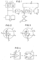
- the inventive device according to FIG. 1 has a plurality of light receivers 1, which are each connected to an equal-current compensation circuit 2.
- the output signals of both light receivers 1 are supplied to a switch arrangement 3, which is designed, for example, as a multiplexer, the number of inputs of the switch arrangement 3 corresponding to the number of light receivers 1.
- a switch arrangement 3 which is designed, for example, as a multiplexer, the number of inputs of the switch arrangement 3 corresponding to the number of light receivers 1.
- either output signal of the light receiver 1 can optionally be placed on the output of the switch arrangement 3.
- the output of the switch assembly 3 is supplied to an input of a mixer 4, wherein a further input of the mixer 4 is connected to the output of a local oscillator 5.
- the local oscillator 5 in turn does not only act on the further input of the mixer 4, but also on a light transmitter 6, which emits a pulsed light signal whose frequency corresponds to the frequency of the local oscillator 5.
- the mixing stage 4 has two outputs which act on an integrating stage 7 whose output is coupled to an evaluation unit 8.
- Mixing stage 4, integrating stage 7 and evaluation unit 8 are controlled by a control unit 9.
- the local oscillator 5 sends a clock signal both to the mixing stage 4 and to the light transmitter 6, these two clock signals being either identical or having a known phase relation to one another.
- the light transmitter 6 emits a correspondingly timed light signal, which can be guided, for example, over a measuring path and a reference path. Due to the light transit time, the light signal passed over the reference path always experiences a constant delay because the length of the reference path does not change. The delay experienced by the light signal transmitted over the measuring path, on the other hand, depends on the length of the measuring path. This delay is then ultimately used to determine the length of the test section.
- each of the two receivers 1 receives the over the measuring path and the other of the two light receivers 1 receives the sent over the reference path light signal, each of the two receivers 1 is coupled to a DC compensation circuit 2, each for the elimination of DC interference signals and low-frequency interference signals are responsible.
- the switch arrangement 3 causes selectively only one of the two signals received by the light receivers 1 to be switched through to the mixing stage 4.
- the switch arrangement 3 therefore, the signal associated with the measuring path and the signal associated with the reference path can be switched to the mixing stage 4 alternately.
- the function of the mixing stage 4 will be explained below with reference to FIGS. 2, 3 and 5.
- the mixing stage 4 subsequent integrating 7 will be explained below with reference to FIGS. 4 and 8.
- FIG. 2 shows the mixing stage 4 according to FIG. 1, which is supplied with the signal a from the switch arrangement 3 on the one hand and with the signal b from the local oscillator 5 on the other hand.
- the signal a is branched to the inputs of two parallel switches 10, 11 whose outputs form the two output signals e and d of the mixer 4.
- the switch 10 is controlled by the signal b of the local oscillator 5, d. h., The switch 10 is opened when the signal b of the local oscillator 5 is "0" and it is closed when this signal b is "1".
- the signal b of the local oscillator 5 is further applied to an inverter 12 whose output signal c controls the switch 11. Accordingly, the switch 11 is always open when the switch 10 is closed and vice versa.
- FIG. 3 shows an arrangement corresponding to FIG. 2, in which, in contrast to FIG. 2, only field-effect transistors 10 ', 11' are used instead of the switches 10, 11 '.
- the base of the field effect transistors 10 ', 11' is acted upon in accordance with FIG. 2 with the signals b and c, which may in this case, for example, also have a sinusoidal shape, so that the mixing stage 4 ultimately no hard switching, but only a sine wave modulation of Signal a causes.
- FIG. 4 shows a block diagram of an integrating stage 7 embodied as an active element 13, which is supplied with the output signals e and d of the mixing stage 4.
- the active element 13 forms the integrals of the two signals e and d, then subtracts these integrals from each other and provides as an output signal the difference signal obtained by said subtraction.
- the active element 13 described is also shown again divided into its components in FIG. 4. From this representation, it is apparent that the signals d and e are respectively supplied to separate integrating stages. The output signals f and g of these two integrating stages are applied to the two inputs of a differential element whose output signal h represents the difference between the two signals f and g.
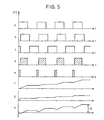
- FIG. 5 shows the time courses of the signals a to h during operation of an arrangement according to FIG. 1 in that state of the switch arrangement 3 in which the light signal transmitted over the measuring path is assigned to the signal a.
- the current signal a delivered by the light receiver 1 and the voltage signal b delivered by the local oscillator have substantially the same frequency and the same pulse duration, but the phase of both signals is shifted relative to each other over the measuring path due to the light propagation time.
- the signal c only provides the inverted signal b, this inversion being effected by the inverter 12 ( Figures 2 and 3).
- the signal a is always switched to the output d when the signal b of the local oscillator 5 the value "1 " having. Accordingly, the signal d is always “1” when both the signal a and the signal b are “1".
- the output signal e of the mixer 4 on the other hand, always assumes the value "1" when both the signal a and the signal c have the value "1", since the switch 11 or the field effect transistor 11 'is connected to the inverse signal c of the Local oscillator 5 is acted upon.
- the integrating stage 7 following the mixing stage 4 forms the two integrals f and g of the signals d and e and then subtracts these integrals from one another, whereby the signal h is obtained.
- the amplitude A of this, supplied by the integrator 7 differential signal h is thus dependent on the degree of phase shift or the cosine of the phase shift between the two signals a and b and, accordingly, the light transit time of the light emitted from the light transmitter 6 over the measuring path light signal.
- the pulses of the signal a would be slightly shifted to the right, whereas the signals b and c would remain unchanged. Accordingly, the pulses of the signal d would be slightly wider and the pulses of the signal e slightly narrower, so that the difference of the two integral signals would change accordingly.
- Fig. 6 shows the amplitude / phase relationship of two possible output signals of the integrator 7. Both signals are each assigned to equally long measuring paths, d. That is, the phase shift to be determined between the signals a and b (FIG. 1) is the same with respect to the two signals shown in FIG. Accordingly, both signals also have an identical zero crossing.
- Fig. 6 thus illustrates that regardless of the amplitude by the determination of the zero crossing always the correct phase relationship can be determined.
- Fig. 7 illustrates that asymmetries between the two channels of the mixer 4 can be compensated by the fact that the signals supplied to the integrator d and e are cyclically interchanged, so that at the output of the integrator 7, two different signals 14 and 15 are obtained. By the averaging of these two signals 14 and 15, the signal 16 ultimately used for the evaluation is then obtained, whose zero crossing lies between the zero crossings of the signals 14 and 15 and thus compensates for asymmetries.
- FIG. 8 shows an integrating stage 7, which has a first multiplexer 17, whose two inputs are supplied with the signals e and d supplied by the mixing stage 4.
- the outputs of the multiplexer 17 are connected to the inputs of another multiplexer 18, which has two outputs, which are fed to an active difference-forming integrator 23.
- the output signal of this integrator 8 forms the output signal of the entire integrating stage 7 according to FIG. 8.
- Each connecting line between an output of the multiplexer 17 and an input of the multiplexer 18 is associated with a (passive) capacitor 19, 20, 21, 22, wherein more arbitrarily more connecting lines and, accordingly, any number of more capacitors can be provided here.
- Half of the capacitors 19 to 22 are assigned to the input signal d and the other half to the input signal e.
- Each clock of the input signal e or d causes a capacitor 19 to 22 associated with the respective input signal to be charged accordingly, with the next clock of the input signal e or d leading to the charging of a further capacitor 19 to 22.
- each clock of each input signal is stored in respective different capacitors 19 to 22, so that none of the capacitors 19 to 22 reaches its capacity limit.
- the charges of the capacitors 19 to 22 are then selectively fed successively or in groups via the multiplexer 18 to the integrator 23, which generates the output signal of the integrating stage 7 from these charges.
Landscapes
- Engineering & Computer Science (AREA)
- Computer Networks & Wireless Communication (AREA)
- Physics & Mathematics (AREA)
- General Physics & Mathematics (AREA)
- Radar, Positioning & Navigation (AREA)
- Remote Sensing (AREA)
- Optical Communication System (AREA)
- Optical Radar Systems And Details Thereof (AREA)
- Gyroscopes (AREA)
- Investigating Or Analysing Materials By Optical Means (AREA)
- Semiconductor Lasers (AREA)
- Measurement Of Unknown Time Intervals (AREA)
- Photometry And Measurement Of Optical Pulse Characteristics (AREA)
Description
- Die Erfindung betrifft eine Vorrichtung zur Ermittlung der Lichtlaufzeit mit einem von einem Oszillator beaufschlagten Lichtsender, einem Lichtempfänger, einer Mischstufe, sowie einer Auswerteeinheit, wobei ein Eingang der Mischstufe von einem Oszillator-Spannungssignal beaufschlagt ist.
- Derartige Vorrichtungen werden beispielsweise in Abstandsmeßgeräten eingesetzt. Hierbei ist es üblich, das einen Photostrom liefernde Ausgangssignal des Lichtempfängers einem Verstärker zuzuführen und mit dem Ausgangssignal des Verstärkers, welches als Spannungssignal vorliegt, einen weiteren Eingang der Mischstufe zu beaufschlagen. Somit liegen an der Mischstufe zwei Spannungssignale, nämlich das Ausgangssignal des Verstärkers sowie das Oszillator-Spannungssignal an.
- Das Ausgangssignal der Mischstufe wird anschließend einer Integrierstufe zugeführt, wobei die Phase des Ausgangssignals der Integrierstufe in einer definierten Beziehung zu der zu ermittelnden Lichtlaufzeit steht.
- Diese bekannten Systeme sind mit dem Nachteil behaftet, daß der erwähnte Verstärker einen amplituden- und temperaturabhängigen Phasengang aufweist, welcher nur mit hohem Aufwand und oftmals auch nur in unzureichender Weise vom gesuchten Phasengang des empfangenen Lichtsignals trennbar ist. Zudem begrenzen die Rauschbeiträge des Verstärkers die Phasenauflösung der bekannten Vorrichtungen.
- Eine Aufgabe der Erfindung besteht darin, eine Vorrichtung der eingangs genannten Art derart weiterzubilden, daß die mit dem Verstärker verbundenen Nachteile, nämlich dessen Phasengang und dessen Rauschbeiträge, eliminiert werden.
- Erfindungsgemäß wird diese Aufgabe dadurch gelöst, daß der den Photostrom liefernde Ausgang des Lichtempfängers ohne die Zwischenschaltung eines ein Spannungssignal liefernden Verstärkers einen weiteren Eingang der Mischstufe beaufschlagt, wobei der weitere Eingang der Mischstufe zur Verarbeitung eines Stromsignals geeignet ist.
- Im Gegensatz zum Stand der Technik wird die Mischstufe erfindungsgemäß also zum einen mit dem Oszillator-Spannungssignal und zum anderen mit dem einen Photostrom liefernden Ausgangssignal des Lichtempfängers beaufschlagt, so daß der Mischstufe letztlich ein Spannungs- und ein Stromsignal zugeführt werden. Da erfindungsgemäß also kein Verstärker eingesetzt wird, welcher das einen Photostrom liefernde Ausgangssignal des Lichtempfängers in ein Spannungssignal umsetzt, lassen sich die eingangs erwähnten Nachteile des Verstärkers vollständig vermeiden. Dies wirkt sich insbesondere deshalb besonders positiv aus, da das Ausgangssignal des Lichtempfängers meist einen sehr hohen, oftmals bis zu sechs Zehnerpotenzen reichenden Amplituden-Dynamikbereich besitzt, so daß bei großen Eingangssignalen der Phasengang und bei kleinen Eingangssignalen das Rauschen des bisher benötigten Verstärkers besonders störend wirkten.
- Weitere Vorteile der Erfindung werden nachfolgend noch im Zusammenhang mit bevorzugten Ausführungsformen beschrieben.
- Von Vorteil ist es, wenn die Mischstufe zwei, insbesondere als jeweils ein Feldeffektransistor ausgebildete Schalter aufweist, wobei der jeweilige Schalterzustand durch das Oszillatorsignal steuerbar ist. In diesem Fall werden also beide Schalter durch Beaufschlagung des vom Oszillator gelieferten Spannungssignals mit der Frequenz des Oszillators geöffnet und geschlossen. Dabei wird bevorzugt der eine Schalterzustand durch das Oszillatorsignal und der andere Schalterzustand durch das invertierte Oszillatorsignal gesteuert, so daß beide Schalter ein zueinander inverses Schaltverhalten aufweisen. Die Eingänge beider Schalter können gemeinsam mit dem den Photostrom liefernden Ausgang des Lichtempfängers verbunden werden, so daß bedingt durch die erwähnte Steuerung der Schalter je nach Phasenlage der Photostrom des Lichtempfängers teilweise über den einen und teilweise über den anderen Schalter fließt, was bedeutet, daß an den Ausgängen der Mischstufe, die durch die Ausgänge der beiden Schalter gebildet sind, abwechselnd das Ausgangssignal des Lichtempfänger anliegt. Aus den beiden Ausgangssignalen der Mischstufe läßt sich anschließend der Phasengang des Ausgangssignals des Lichtempfängers gegenüber dem Oszillator-Spannungssignal ermitteln, was nachfolgend noch erläutert wird.
- Die erfindungsgemäße Vorrichtung arbeitet bevorzugt mit einem ein Rechteck-Taktsignal liefernden Oszillator, welcher sowohl die Mischstufe als auch den Lichtsender beaufschlagt, so daß der Lichtsender ein entsprechend gepulstes Lichtsignal abgibt. Alternativ können Mischstufe und Lichtsender auch mit voneinander unterschiedlichen Oszillator-Signalen beaufschlagt werden, die jedoch eine definierte Phasenbeziehung zueinander besitzen müssen, um so einen Rückschluß auf die Lichtlaufzeit zuzulassen.
- Durch die vorstehend beschriebene Ausbildung der Mischstufe mit zwei Schaltern bzw. zwei Feldeffekttransistoren läßt sich ein linearer Mischvorgang erreichen, welcher im Gegensatz zum Stand der Technik über den gesamten Amplituden-Dynamikbereich allenfalls einen vernachlässigbaren amplitudenabhängigen Phasengang aufweist. Durch einen solchen Phasengang hervorgerufene Fehler werden somit vollständig eliminiert.
- Die beiden Ausgänge der Mischstufe können mit einer Integrierstufe verbunden werden, wobei die Integrierstufe zum separaten Integrieren beider Schalterausgangssignale und insbesondere auch zur Differenzbildung zwischen den beiden integrierten Schalterausgangssignalen ausgelegt sein kann. Die Funktionsweise einer solchen Integrierstufe wird nachstehend noch im Rahmen der Figurenbeschreibung näher erläutert.
- Grundsätzlich kann die Integrierstufe als rein aktives oder als kombiniert passives/aktives Element ausgebildet werden.
- Falls die Integrierstufe als kombiniert passives/aktives Element ausgebildet werden soll, ist es bevorzugt, wenn sie zumindest einen, von den beiden Schalterausgangssignalen beaufschlagten Multiplexer aufweist, dessen Ausgänge mit dem Eingang jeweils eines Kondensators (passives Element) verbunden sind, wobei die Ausgänge des Kondensators jeweils einen Eingang eines weiteren Multiplexers beaufschlagen, welcher seinerseits zumindest zwei Ausgänge aufweist. Dabei können die beiden Ausgänge des weiteren Multiplexers mit den Eingängen eines insbesondere integrierenden aktiven Differenzelements verbunden werden. Auch die Funktionsweise einer solchen Integrierstufe wird nachfolgend anhand der Figurenbeschreibung noch näher erläutert.
- Besonders vorteilhaft arbeitet die erfindungsgemäße Vorrichtung dann, wenn eine Mehrzahl von Lichtempfängern über ein oder mehrere Schaltelemente mit dem einen Eingang der Mischstufe gekoppelt werden. Auf diese Weise läßt sich die erfindungsgemäße Vorrichtung mehrkanalig ausführen, wobei wahlweise jeweils ein Empfangskanal auf die Mischstufe aufschaltbar ist. Da keiner der Kanäle zwischen Lichtempfänger und Mischstufe einen Verstärker benötigt, lassen sich die erfindungsgemäßen Vorteile für jeden einzelnen Kanal verwirklichen.
- Insbesondere ist eine zumindest zweikanalige Ausbildung der erfindungsgemäßen Vorrichtung sinnvoll, da auf diese Weise - neben einem Meßkanal - ein Referenzkanal zur Verfügung steht, welcher beispielsweise einem gehäuseinternen Referenzlichtpfad zugeordnet ist und welcher dazu dient, Temperaturabhängigkeiten der erfindungsgemäßen Vorrichtung zu eliminieren. Weder hinsichtlich des Referenzlichtempfängers noch hinsichtlich des für den Meßkanal zuständigen Lichtempfängers müssen in diesem Fall die aus dem Stand der Technik bekannten Nachteile von sich unterschiedlich verhaltenden Verstärkern in Kauf genommen werden, da solche Verstärker erfindungsgemäß nicht mehr nötig sind.
- Von Vorteil ist es, wenn jeder Lichtempfänger mit je einer Gleichstrom-Kompensationsschaltung verbunden ist, so daß auf diese Weise weitgehend konstante bzw. niederfrequente Störsignale für jeden Lichtempfänger separat eliminiert werden können. Alternativ ist es auch möglich, daß jeder Lichtempfänger mit einer gemeinsamen Gleichstrom-Kompensationsschaltung verbindbar ist.
- Weitere bevorzugte Ausführungsformen der Erfindung sind in den Unteransprüchen beschrieben.
- Die Erfindung wird nachfolgend anhand von Ausführungsbeispielen unter Bezugnahme auf die Zeichnungen erläutert; in diesen zeigen:
- Fig. 1
- ein Blockschaltbild einer möglichen Ausführungsform einer erfindungsgemäßen Vorrichtung,
- Fig. 2
- ein Schaltbild einer erfindungsgemäßen Mischstufe gemäß einer ersten Ausführungsform,
- Fig. 3
- ein Schaltbild einer erfindungsgemäßen Mischstufe gemäß zweiten Ausführungsform,
- Fig. 4
- eine erste Ausführungsform einer erfindungsgemäß zum Einsatz gelangenden Integrierstufe,
- Fig. 5
- die Strom- bzw. Spannungsverläufe an den Ein- und Ausgängen einer Mischstufe gemäß Fig. 3,
- Fig. 6
- die Spannungs-Phasenbeziehung des Ausgangssignals der Integrierstufe gemäß Fig. 4,
- Fig. 7
- die Spannungs-Phasenbeziehung zweier unterschiedlicher Ausgangssignale der Integrierstufe gemäß Fig. 4, die zum Ausgleich von Asymmetrien der beiden Mischkanäle der erfindungsgemäßen Mischstufe herangezogen werden können, und
- Fig. 8
- eine zweite Ausführungsform einer erfindungsgemäß zum Einsatz gelangenden Integrierstufe.
- Die erfindungsgemäße Vorrichtung gemäß Fig. 1 weist eine Mehrzahl von Lichtempfängern 1 auf, welche jeweils mit einer Gleichtstrom-Kompensationsschaltung 2 verbunden sind. Die Ausgangssignale beider Lichtempfänger 1 sind einer beispielsweise als Multiplexer ausgebildeten Schalteranordnung 3 zugeführt, wobei die Anzahl der Eingänge der Schalteranordnung 3 der Anzahl der Lichtempfänger 1 entspricht. Mittels der Schalteranordnung 3 kann wahlweise jedes Ausgangssignal der Lichtempfänger 1 auf den Ausgang der Schalteranordnung 3 gelegt werden.
- Der Ausgang der Schalteranordnung 3 ist einem Eingang einer Mischstufe 4 zugeführt, wobei ein weiterer Eingang der Mischstufe 4 mit dem Ausgang eines Lokaloszillators 5 verbunden ist. Der Lokaloszillator 5 seinerseits beaufschlagt nicht nur den weiteren Eingang der Mischstufe 4, sondern ebenfalls einen Lichtsender 6, welcher ein gepulstes Lichtsignal aussendet, dessen Frequenz der Frequenz des Lokaloszillators 5 entspricht.
- Die Mischstufe 4 besitzt zwei Ausgänge, welche eine Integrierstufe 7 beaufschlagen, deren Ausgang mit einem Auswerte-Baustein 8 gekoppelt ist.
- Mischstufe 4, Integrierstufe 7 sowie Auswerte-Baustein 8 werden von einer Steuereinheit 9 kontrolliert.
- Beim Betrieb der Vorrichtung gemäß Fig. 1 sendet der Lokaloszillator 5 ein Taktsignal sowohl an die Mischstufe 4 als auch an den Lichtsender 6, wobei diese beiden Taktsignale entweder identisch sind oder eine bekannte Phasenbeziehung zueinander aufweisen. Der Lichtsender 6 sendet ein entsprechend getaktetes Lichtsignal aus, welches beispielsweise über eine Meßstrecke und eine Referenzstrecke geführt werden kann. Das über die Referenzstrecke geführte Lichtsignal erfährt bedingt durch die Lichtlaufzeit immer eine konstante Verzögerung, da sich die Länge der Referenzstrecke nicht ändert. Die Verzögerung, die das über die Meßstrecke gesendete Lichtsignal erfährt, ist hingegen abhängig von der Länge der Meßstrecke. Diese Verzögerung wird dann letztlich zur Bestimmung der Länge der Meßstrecke herangezogen.
- Einer der beiden Lichtempfänger 1 empfängt das über die Meßstrecke und der andere der beiden Lichtempfänger 1 empfängt das über die Referenzstrecke gesandte Lichtsignal, wobei jeder der beiden Empfänger 1 mit einer Gleichstrom-Kompensationsschaltung 2 gekoppelt ist, welche jeweils für die Beseitigung von Gleichstrom-Störsignalen und niederfrequenten Störsignalen verantwortlich sind.
- Die Schalteranordnung 3 bewirkt, daß wahlweise immer nur eines der beiden von den Lichtempfängern 1 empfangenen Signale zur Mischstufe 4 durchgeschaltet wird. Mittels der Schalteranordnung 3 können also abwechselnd das der Meßstrecke und das der Referenzstrecke zugeordnete Signal auf die Mischstufe 4 aufgeschaltet werden.
- Die Funktion der Mischstufe 4 wird nachfolgend noch anhand der Fig. 2, 3 und 5 erläutert. Die der Mischstufe 4 nachfolgende Integrierstufe 7 wird nachfolgend noch anhand der Fig. 4 und 8 erläutert.
- Fig. 2 zeigt die Mischstufe 4 gemäß Fig. 1, der zum einen das Signal a von der Schalteranordnung 3 und zum anderen das Signal b vom Lokaloszillator 5 zugeführt wird. Das Signal a wird zu den Eingängen von zwei parallel angeordneten Schaltern 10, 11 verzweigt, deren Ausgänge die beiden Ausgangssignale e und d der Mischstufe 4 bilden.
- Der Schalter 10 wird durch das Signal b des Lokaloszillators 5 gesteuert, d. h., der Schalter 10 ist geöffnet, wenn das Signal b des Lokaloszillators 5 "0" ist und er ist geschlossen, wenn dieses Signal b "1" ist.
- Das Signal b des Lokaloszillators 5 wird weiterhin auf einen Inverter 12 gelegt, dessen Ausgangssignal c den Schalter 11 steuert. Dementsprechend ist der Schalter 11 immer dann geöffnet, wenn der Schalter 10 geschlossen ist und umgekehrt.
- Fig. 3 zeigt eine Fig. 2 entsprechende Anordnung, bei der im Unterschied zu Fig. 2 lediglich anstelle der Schalter 10, 11 Feldeffekttransistoren 10', 11' zum Einsatz gelangen. Die Basis der Feldeffektransistoren 10', 11' ist dabei entsprechend Fig. 2 mit den Signalen b und c beaufschlagt, die in diesem Fall z.B. auch eine Sinusform aufweisen können, so daß auch die Mischstufe 4 letztlich kein hartes Schalten, sondern lediglich eine Sinusmodulation des Signals a bewirkt.
- Fig. 4 zeigt ein Blockschaltbild einer als aktives Element 13 ausgebildeten Integrierstufe 7, die mit den Ausgangssignalen e und d der Mischstufe 4 beaufschlagt ist. Das aktive Element 13 bildet die Integrale der beiden Signale e und d, subtrahiert diese Integrale anschließend voneinander und liefert als Ausgangssignal das durch die genannte Subtraktion erhaltene Differenzsignal.
- Das beschriebene aktive Element 13 ist in Fig. 4 auch nochmals aufgeteilt in seine Bestandteile gezeigt. Aus dieser Darstellung geht hervor, daß die Signale d und e jeweils separaten Integrierstufen zugeführt werden. Die Ausgangssignale f und g dieser beiden Integrierstufen sind an die beiden Eingänge eines Differenzelements angelegt, dessen Ausgangssignal h die Differenz zwischen den beiden Signalen f und g darstellt.
- Fig. 5 zeigt die Zeitverläufe der Signale a bis h beim Betrieb einer Anordnung gemäß Fig. 1 in demjenigen Zustand der Schalteranordnung 3, bei dem das über die Meßstrecke gesendete Lichtsignal dem Signal a zugeordnet ist.
- Das vom Lichtempfänger 1 gelieferte Stromsignal a und das vom Lokaloszillator gelieferte Spannungssignal b weisen im wesentlichen die gleiche Frequenz und die gleiche Impulsdauer auf, wobei jedoch die Phase beider Signale aufgrund der Lichtlaufzeit über die Meßstrecke zueinander verschoben ist.
- Das Signal c stellt lediglich das invertierte Signal b da, wobei diese Invertierung durch den Inverter 12 (Fig. 2 und 3) bewirkt wird.
- Aufgrund der in Verbindung mit den Fig. 2 und 3 erläuterten Anordnung der Schalter 10, 11 bzw. der Feldeffekttransistoren 10', 11' wird das Signal a immer dann auf den Ausgang d durchgeschaltet, wenn das Signal b des Lokaloszillators 5 den Wert "1" aufweist. Dementsprechend ist das Signal d immer dann "1", wenn sowohl das Signal a als auch das Signal b den Wert "1" aufweisen.
- Das Ausgangssignal e der Mischstufe 4 hingegen nimmt immer dann den Wert "1" an, wenn sowohl das Signal a als auch das Signal c den Wert "1" aufweisen, da der Schalter 11 bzw. der Feldeffektransistor 11' mit dem inversen Signal c des Lokaloszillators 5 beaufschlagt ist.
- Die der Mischstufe 4 nachfolgende Integrierstufe 7 bildet die beiden Integrale f und g der Signale d und e und subtrahiert diese Integrale dann voneinander, wodurch das Signal h erhalten wird. Die Amplitude A dieses, von der Integrierstufe 7 gelieferten Differenzsignals h ist somit abhängig vom Grad der Phasenverschiebung bzw. vom Cosinus der Phasenverschiebung zwischen den beiden Signalen a und b und dementsprechend auch von der Lichtlaufzeit des vom Lichtsender 6 über die Meßstrecke gesandten Lichtsignals.
- Wenn beispielsweise das über die Meßstrecke gesandte Lichtsignal aufgrund einer längeren Strecke eine geringfügig stärkere Verzögerung erfahren würde, als in Fig. 5 dargestellt, wären die Impulse des Signals a leicht nach rechts verschoben, wohingegen die Signale b und c unverändert blieben. Dementsprechend wären die Impulse des Signals d etwas breiter und die Impulse des Signals e etwas schmäler, so daß sich die Differenz der beiden Integralsignale entsprechend verändern würde.
- Fig. 6 zeigt die Amplituden/Phasenbeziehung zweier möglicher Ausgangssignale der Integrierstufe 7. Beide Signale sind jeweils gleich langen Meßstrecken zugeordnet, d. h., die zu ermittelnde Phasenverschiebung zwischen den Signalen a und b (Fig. 1) ist bezüglich beider in Fig. 6 dargestellter Signale gleich groß. Dementsprechend besitzen beide Signale auch einen identischen Nulldurchgang.
- Der Unterschied zwischen den beiden in Fig. 6 dargestellten Signalen besteht lediglich darin, daß das durchgezogen gezeichnete Signal von einem Eingangssignal a höherer und das gepunktet gezeichnete Signal von einem Eingangssignal a niedrigerer Amplitude stammt. Fig. 6 veranschaulicht somit, daß unabhängig von der Amplitude durch die Bestimmung des Nulldurchgangs immer die korrekte Phasenbeziehung ermittelt werden kann.
- Fig. 7 veranschaulicht, daß Asymmetrien zwischen den beiden Kanälen der Mischstufe 4 dadurch ausgeglichen werden können, daß die der Integrierstufe zugeführten Signalen d und e zyklisch miteinander vertauscht werden, so daß am Ausgang der Integrierstufe 7 zwei unterschiedliche Signale 14 und 15 erhalten werden. Durch die Mittelung dieser beiden Signale 14 und 15 wird dann das letztlich zur Auswertung herangezogene Signal 16 erhalten, dessen Nulldurchgang zwischen den Nulldurchgängen der Signale 14 und 15 liegt und somit Asymmetrien kompensiert.
- Fig. 8 zeigt eine Integrierstufe 7, welche einen ersten Multiplexer 17 aufweist, dessen beide Eingänge mit den von der Mischstufe 4 gelieferten Signalen e und d beaufschlagt sind. Die Ausgänge des Multiplexers 17 sind mit den Eingängen eines weiteren Multiplexers 18 verbunden, welcher zwei Ausgänge besitzt, die einem aktiven differenzbildenden Integrator 23 zugeführt sind. Das Ausgangssignal dieses Integrators 8 bildet das Ausgangssignal der gesamten Integrierstufe 7 gemäß Fig. 8.
- Jeder Verbindungsleitung zwischen einem Ausgang des Multiplexers 17 und einem Eingang des Multiplexers 18 ist ein (passiver) Kondensator 19, 20, 21, 22 zugeordnet, wobei hier ohne weiteres beliebig mehr Verbindungsleitungen und dementsprechend auch beliebig mehr Kondensatoren vorgesehen sein können.
- Die Hälfte der Kondensatoren 19 bis 22 sind dem Eingangssignal d und die anderen Hälfte dem Eingangssignal e zugeordnet. Jeder Takt des Eingangssignals e bzw. d führt dazu, daß ein dem jeweiligen Eingangssignal zugeordneter Kondensator 19 bis 22 entsprechend aufgeladen wird, wobei der nächste Takt des Eingangssignals e bzw. d zum Aufladen eines weiteren Kondensators 19 bis 22 führt. Somit wird jeder Takt jedes Eingangssignals in jeweils unterschiedlichen Kondensatoren 19 bis 22 gespeichert, so daß keiner der Kondensatoren 19 bis 22 an seine Kapazitätsgrenze gelangt.
- Die Ladungen der Kondensatoren 19 bis 22 werden dann gezielt nacheinander oder in Gruppen über den Multiplexer 18 dem Integrator 23 zugeführt, welcher aus diesen Ladungen das Ausgangssignal der Integrierstufe 7 erzeugt.
-
- 1
- Lichtempfänger
- 2
- Gleichstrom-Kompensationsschaltung
- 3
- Schalteranordnung
- 4
- Mischstufe
- 5
- Lokaloszillator
- 6
- Lichtsender
- 7
- Integrierstufe
- 8
- Auswerte-Baustein
- 9
- Steuereinheit
- 10
- Schalter
- 10'
- Feldeffekttransistor
- 11
- Schalter
- 11'
- Feldeffekttransistor
- 12
- Invertierer
- 13
- aktives Element
- 14
- Signal
- 15
- Signal
- 16
- Signal
- 17
- Multiplexer
- 18
- Multiplexer
- 19
- Kondensator
- 20
- Kondensator
- 21
- Kondensator
- 22
- Kondensator
- 23
- Integrator
Claims (12)
- Vorrichtung zur Ermittlung der Lichtlaufzeit mit einem von einem Oszillator (5) beaufschlagten Lichtsender (6), einem Lichtempfänger (1), einer Mischstufe (4), sowie einer Auswerteeinheit (7, 8, 9), wobei ein Eingang der Mischstufe von einem Oszillator-Spannungssignal (b) beaufschlagt ist,
dadurch gekennzeichnet,
dass der den Photostrom liefernde Ausgang des Lichtempfängers (1) ohne die Zwischenschaltung eines ein Spannungssignal liefernden Verstärkers einen weiteren Eingang der Mischstufe (4) beaufschlagt, wobei der weitere Eingang der Mischstufe (4) zur Verarbeitung eines Stromsignals geeignet ist. - Vorrichtung nach Anspruch 1,
dadurch gekennzeichnet,
daß die Mischstufe (4) zwei Schalter (10, 11) aufweist, wobei der jeweilige Schalterzustand durch das Oszillatorsignal (b, c) steuerbar ist. - Vorrichtung nach Anspruch 2,
dadurch gekennzeichnet,
daß ein Schalterzustand durch das Oszillatorsignal (b) und der andere Schalterzustand durch das invertierte Oszillatorsignal (c) steuerbar ist. - Vorrichtung nach Anspruch 2 oder 3,
dadurch gekennzeichnet,
daß die Eingänge beider Schalter (10, 11) mit dem den Photostrom liefernden Ausgang des Lichtempfängers (1) verbunden sind. - Vorrichtung nach Anspruch 2 bis 4,
dadurch gekennzeichnet,
daß beide Schalter als jeweils ein Feldeffekttransistor (10', 11') ausgebildet sind. - Vorrichtung nach Anspruch 2 bis 5,
dadurch gekennzeichnet,
daß die Ausgänge beider Schalter (10, 10', 11, 11') mit einer Integrierstufe (7) verbunden sind. - Vorrichtung nach Anspruch 6,
dadurch gekennzeichnet,
daß die Integrierstufe (7) zur separaten Integrierung beider Schalterausgangssignale (d, e) und insbesondere auch zur Differenzbildung zwischen den beiden integrierten Schalterausgangssignalen (d, e) ausgelegt ist. - Vorrichtung nach Anspruch 6 oder 7,
dadurch gekennzeichnet,
daß die Integrierstufe (7) als rein aktives oder als kombiniert passives/aktives Element ausgebildet ist. - Vorrichtung nach Anspruch 6 bis 8,
dadurch gekennzeichnet,
daß die Integrierstufe (7) zumindest einen, von den beiden Schalterausgangssignalen (d, e) beaufschlagten Multiplexer (17) aufweist, dessen Ausgänge mit dem Eingang jeweils eines Kondensators (19 bis 22) verbunden sind, wobei die Ausgänge der Kondensatoren (19 bis 22) jeweils einen Eingang eines weiteren Multiplexers (18) beaufschlagen, welcher seinerseits zumindest zwei Ausgänge aufweist. - Vorrichtung nach Anspruch 9,
dadurch gekennzeichnet,
daß die beiden Ausgänge des weiteren Multiplexers (18) mit den Eingängen eines insbesondere integrierenden Differenzelements (23) verbunden sind. - Vorrichtung nach einem der vorherigen Ansprüche,
dadurch gekennzeichnet,
daß eine Mehrzahl von Lichtempfängern (1) über ein oder mehrere Schaltelemente (3) mit dem Eingang der Mischstufe (4) koppelbar sind. - Vorrichtung nach einem der vorherigen Ansprüche,
dadurch gekennzeichnet,
daß jeder Lichtempfänger (1) mit je einer Gleichstrom-Kompensationsschaltung (2) verbunden ist, oder daß jeder Lichtempfänger (1) mit einer gemeinsamen Gleichstrom-Kompensationsschaltung verbindbar ist.
Applications Claiming Priority (2)
| Application Number | Priority Date | Filing Date | Title |
|---|---|---|---|
| DE10010212 | 2000-03-02 | ||
| DE10010212A DE10010212A1 (de) | 2000-03-02 | 2000-03-02 | Vorrichtung zur Ermittlung der Lichtlaufzeit |
Publications (3)
| Publication Number | Publication Date |
|---|---|
| EP1132726A2 EP1132726A2 (de) | 2001-09-12 |
| EP1132726A3 EP1132726A3 (de) | 2004-10-20 |
| EP1132726B1 true EP1132726B1 (de) | 2007-05-09 |
Family
ID=7633263
Family Applications (1)
| Application Number | Title | Priority Date | Filing Date |
|---|---|---|---|
| EP01105034A Expired - Lifetime EP1132726B1 (de) | 2000-03-02 | 2001-03-01 | Vorrichtung zur Ermittlung der Lichtlaufzeit |
Country Status (3)
| Country | Link |
|---|---|
| EP (1) | EP1132726B1 (de) |
| AT (1) | ATE362097T1 (de) |
| DE (2) | DE10010212A1 (de) |
Families Citing this family (4)
| Publication number | Priority date | Publication date | Assignee | Title |
|---|---|---|---|---|
| EP1522870B1 (de) | 2003-10-06 | 2013-07-17 | Triple-IN Holding AG | Entfernungsmessung |
| DE102006016026A1 (de) * | 2006-04-05 | 2007-10-11 | Sick Ag | Distanzmessvorrichtung |
| EP1901093B1 (de) | 2006-09-15 | 2018-11-14 | Triple-IN Holding AG | Aufnahme von Entfernungsbildern |
| RU2448334C2 (ru) * | 2010-06-23 | 2012-04-20 | Федеральное государственное военное образовательное учреждение высшего профессионального образования Военная академия Ракетных войск стратегического назначения имени Петра Великого МО РФ | Способ проверки отсутствия влияния орбитального движения земли на скорость света |
Family Cites Families (8)
| Publication number | Priority date | Publication date | Assignee | Title |
|---|---|---|---|---|
| US3778159A (en) * | 1970-03-10 | 1973-12-11 | Laser Systems & Electronics | Distance measuring apparatus and method utilizing phase comparison of modulated light beams |
| FR2543690B1 (fr) * | 1983-03-29 | 1986-01-17 | Thomson Csf | Systeme de telemetrie laser et de mesure doppler, a compression d'impulsions |
| DE4002356C2 (de) * | 1990-01-26 | 1996-10-17 | Sick Optik Elektronik Erwin | Abstandsmeßgerät |
| EP0556960A3 (en) * | 1992-02-20 | 1995-02-01 | Optical Metrology Ltd | Measurement apparatus using heterodyne phase conversion techniques |
| DE4328553A1 (de) * | 1993-04-30 | 1994-11-03 | Rudolf Prof Dr Ing Schwarte | Entfernungsmeßgerät nach dem Laufzeitprinzip |
| US6008487A (en) * | 1995-02-02 | 1999-12-28 | Yokogawa Electric Corporation | Optical-fiber inspection device |
| US5844235A (en) * | 1995-02-02 | 1998-12-01 | Yokogawa Electric Corporation | Optical frequency domain reflectometer for use as an optical fiber testing device |
| US5745437A (en) * | 1996-08-05 | 1998-04-28 | Wachter; Eric A. | Method and apparatus for coherent burst ranging |
-
2000
- 2000-03-02 DE DE10010212A patent/DE10010212A1/de not_active Withdrawn
-
2001
- 2001-03-01 EP EP01105034A patent/EP1132726B1/de not_active Expired - Lifetime
- 2001-03-01 AT AT01105034T patent/ATE362097T1/de active
- 2001-03-01 DE DE50112466T patent/DE50112466D1/de not_active Expired - Lifetime
Also Published As
| Publication number | Publication date |
|---|---|
| DE10010212A1 (de) | 2001-09-13 |
| EP1132726A3 (de) | 2004-10-20 |
| ATE362097T1 (de) | 2007-06-15 |
| DE50112466D1 (de) | 2007-06-21 |
| EP1132726A2 (de) | 2001-09-12 |
Similar Documents
| Publication | Publication Date | Title |
|---|---|---|
| EP0793075B1 (de) | Monolithisch integrierte Sensorschaltung | |
| DE69802040T2 (de) | Präzisions-Oszillatorschaltung mit steuerbarem Tastverhältnis und entsprechendes Verfahren | |
| DE69528234T2 (de) | Schaltung und Verfahren zur Erzeugung eines Taktsignals | |
| DE10232346B4 (de) | Schaltungsanordnung und Verfahren zur Datensignalreproduktion | |
| DE2153432A1 (de) | Akustischer Durchflußmesser | |
| DE10130123B4 (de) | Verzögerungsregelkreis zur Erzeugung komplementärer Taktsignale | |
| DE19743298C2 (de) | Impulsformerschaltung | |
| DE102019102132B4 (de) | Schaltung mit Kondensatoren und entsprechendes Verfahren | |
| WO1991020129A1 (de) | Schaltung zur begrenzung der signalanstiegsgeschwindigkeit von ausgangssignalen integrierter schaltkreise | |
| EP0957582B1 (de) | Schaltungsanordnung zur Erzeugung komplementärer Signale | |
| DE68920089T2 (de) | Schaltung zur Verarbeitung eines sich zeitlich ändernden Signals. | |
| EP1156299A1 (de) | Messumformer für potentiometrische Positionssensoren und Verfahren zur Parametrierung | |
| EP1132726A2 (de) | Vorrichtung zur Ermittlung der Lichtlaufzeit | |
| DE102004013093B3 (de) | Empfängerschaltung für ein Gegentaktübertragungsverfahren | |
| EP3180859A1 (de) | Schaltung und verfahren zum auswerten von messsignalen sowie sensorsystem zum kapazitiven erfassen von hindernissen | |
| DE60006453T2 (de) | Ladungspumpe für PLL in integrierter Schaltung | |
| EP0012306A1 (de) | Mehrkanalige Verstärkereinrichtung mit einem Verstärker für zeitlich verschachtelte Schwingungspakete | |
| EP1094328B1 (de) | Magnetfeldsensor mit Kettenleiterfilter | |
| DE19909536C1 (de) | Integrierte Schaltung zur Erzeugung zweier Ausgangstakte mit zeitlich nicht überlappenden Pegeln | |
| DE19841203C1 (de) | Digitale Schaltung | |
| DE10328566B4 (de) | Verfahren und Vorrichtung zum Abtasten eines Datensignals | |
| DE10334805B4 (de) | Analoge Multiplizierschaltung | |
| EP0448744A1 (de) | Taktsynchronisationsschaltung | |
| EP4687298A1 (de) | Verfahren zum abgleichen eines phasenmodulationswandlers und phasenmodulationswandler | |
| DE102020123930B3 (de) | Verfahren zur ISO 26262 konformen Auswertung eines Drucksensorsignals |
Legal Events
| Date | Code | Title | Description |
|---|---|---|---|
| PUAI | Public reference made under article 153(3) epc to a published international application that has entered the european phase |
Free format text: ORIGINAL CODE: 0009012 |
|
| AK | Designated contracting states |
Kind code of ref document: A2 Designated state(s): AT BE CH CY DE DK ES FI FR GB GR IE IT LI LU MC NL PT SE TR |
|
| AX | Request for extension of the european patent |
Free format text: AL;LT;LV;MK;RO;SI |
|
| RIN1 | Information on inventor provided before grant (corrected) |
Inventor name: BLUEMCKE, THOMAS Inventor name: TORABI, BAHRAM, DR. |
|
| PUAL | Search report despatched |
Free format text: ORIGINAL CODE: 0009013 |
|
| AK | Designated contracting states |
Kind code of ref document: A3 Designated state(s): AT BE CH CY DE DK ES FI FR GB GR IE IT LI LU MC NL PT SE TR |
|
| AX | Request for extension of the european patent |
Extension state: AL LT LV MK RO SI |
|
| 17P | Request for examination filed |
Effective date: 20041125 |
|
| AKX | Designation fees paid |
Designated state(s): AT BE CH CY DE DK ES FI FR GB GR IE IT LI LU MC NL PT SE TR |
|
| GRAP | Despatch of communication of intention to grant a patent |
Free format text: ORIGINAL CODE: EPIDOSNIGR1 |
|
| GRAS | Grant fee paid |
Free format text: ORIGINAL CODE: EPIDOSNIGR3 |
|
| RAP1 | Party data changed (applicant data changed or rights of an application transferred) |
Owner name: SICK AG |
|
| GRAA | (expected) grant |
Free format text: ORIGINAL CODE: 0009210 |
|
| AK | Designated contracting states |
Kind code of ref document: B1 Designated state(s): AT BE CH CY DE DK ES FI FR GB GR IE IT LI LU MC NL PT SE TR |
|
| PG25 | Lapsed in a contracting state [announced via postgrant information from national office to epo] |
Ref country code: FI Free format text: LAPSE BECAUSE OF FAILURE TO SUBMIT A TRANSLATION OF THE DESCRIPTION OR TO PAY THE FEE WITHIN THE PRESCRIBED TIME-LIMIT Effective date: 20070509 |
|
| REG | Reference to a national code |
Ref country code: GB Ref legal event code: FG4D Free format text: NOT ENGLISH |
|
| REG | Reference to a national code |
Ref country code: CH Ref legal event code: EP |
|
| REG | Reference to a national code |
Ref country code: IE Ref legal event code: FG4D Free format text: LANGUAGE OF EP DOCUMENT: GERMAN |
|
| REF | Corresponds to: |
Ref document number: 50112466 Country of ref document: DE Date of ref document: 20070621 Kind code of ref document: P |
|
| REG | Reference to a national code |
Ref country code: SE Ref legal event code: TRGR |
|
| GBT | Gb: translation of ep patent filed (gb section 77(6)(a)/1977) |
Effective date: 20070628 |
|
| PG25 | Lapsed in a contracting state [announced via postgrant information from national office to epo] |
Ref country code: ES Free format text: LAPSE BECAUSE OF FAILURE TO SUBMIT A TRANSLATION OF THE DESCRIPTION OR TO PAY THE FEE WITHIN THE PRESCRIBED TIME-LIMIT Effective date: 20070820 |
|
| ET | Fr: translation filed | ||
| NLV1 | Nl: lapsed or annulled due to failure to fulfill the requirements of art. 29p and 29m of the patents act | ||
| REG | Reference to a national code |
Ref country code: IE Ref legal event code: FD4D |
|
| PG25 | Lapsed in a contracting state [announced via postgrant information from national office to epo] |
Ref country code: IE Free format text: LAPSE BECAUSE OF FAILURE TO SUBMIT A TRANSLATION OF THE DESCRIPTION OR TO PAY THE FEE WITHIN THE PRESCRIBED TIME-LIMIT Effective date: 20070509 Ref country code: NL Free format text: LAPSE BECAUSE OF FAILURE TO SUBMIT A TRANSLATION OF THE DESCRIPTION OR TO PAY THE FEE WITHIN THE PRESCRIBED TIME-LIMIT Effective date: 20070509 Ref country code: PT Free format text: LAPSE BECAUSE OF FAILURE TO SUBMIT A TRANSLATION OF THE DESCRIPTION OR TO PAY THE FEE WITHIN THE PRESCRIBED TIME-LIMIT Effective date: 20071009 Ref country code: DK Free format text: LAPSE BECAUSE OF FAILURE TO SUBMIT A TRANSLATION OF THE DESCRIPTION OR TO PAY THE FEE WITHIN THE PRESCRIBED TIME-LIMIT Effective date: 20070509 |
|
| PLBE | No opposition filed within time limit |
Free format text: ORIGINAL CODE: 0009261 |
|
| STAA | Information on the status of an ep patent application or granted ep patent |
Free format text: STATUS: NO OPPOSITION FILED WITHIN TIME LIMIT |
|
| 26N | No opposition filed |
Effective date: 20080212 |
|
| PG25 | Lapsed in a contracting state [announced via postgrant information from national office to epo] |
Ref country code: GR Free format text: LAPSE BECAUSE OF FAILURE TO SUBMIT A TRANSLATION OF THE DESCRIPTION OR TO PAY THE FEE WITHIN THE PRESCRIBED TIME-LIMIT Effective date: 20070810 |
|
| BERE | Be: lapsed |
Owner name: SICK A.G. Effective date: 20080331 |
|
| PG25 | Lapsed in a contracting state [announced via postgrant information from national office to epo] |
Ref country code: MC Free format text: LAPSE BECAUSE OF NON-PAYMENT OF DUE FEES Effective date: 20080331 |
|
| PG25 | Lapsed in a contracting state [announced via postgrant information from national office to epo] |
Ref country code: BE Free format text: LAPSE BECAUSE OF NON-PAYMENT OF DUE FEES Effective date: 20080331 |
|
| PG25 | Lapsed in a contracting state [announced via postgrant information from national office to epo] |
Ref country code: CY Free format text: LAPSE BECAUSE OF FAILURE TO SUBMIT A TRANSLATION OF THE DESCRIPTION OR TO PAY THE FEE WITHIN THE PRESCRIBED TIME-LIMIT Effective date: 20070509 |
|
| PG25 | Lapsed in a contracting state [announced via postgrant information from national office to epo] |
Ref country code: LU Free format text: LAPSE BECAUSE OF NON-PAYMENT OF DUE FEES Effective date: 20080301 |
|
| PG25 | Lapsed in a contracting state [announced via postgrant information from national office to epo] |
Ref country code: TR Free format text: LAPSE BECAUSE OF FAILURE TO SUBMIT A TRANSLATION OF THE DESCRIPTION OR TO PAY THE FEE WITHIN THE PRESCRIBED TIME-LIMIT Effective date: 20070509 |
|
| PGFP | Annual fee paid to national office [announced via postgrant information from national office to epo] |
Ref country code: SE Payment date: 20120322 Year of fee payment: 12 |
|
| PGFP | Annual fee paid to national office [announced via postgrant information from national office to epo] |
Ref country code: AT Payment date: 20120321 Year of fee payment: 12 |
|
| PGFP | Annual fee paid to national office [announced via postgrant information from national office to epo] |
Ref country code: GB Payment date: 20130318 Year of fee payment: 13 Ref country code: FR Payment date: 20130329 Year of fee payment: 13 Ref country code: CH Payment date: 20130319 Year of fee payment: 13 |
|
| REG | Reference to a national code |
Ref country code: SE Ref legal event code: EUG |
|
| PG25 | Lapsed in a contracting state [announced via postgrant information from national office to epo] |
Ref country code: SE Free format text: LAPSE BECAUSE OF NON-PAYMENT OF DUE FEES Effective date: 20130302 |
|
| REG | Reference to a national code |
Ref country code: AT Ref legal event code: MM01 Ref document number: 362097 Country of ref document: AT Kind code of ref document: T Effective date: 20130301 |
|
| PG25 | Lapsed in a contracting state [announced via postgrant information from national office to epo] |
Ref country code: AT Free format text: LAPSE BECAUSE OF NON-PAYMENT OF DUE FEES Effective date: 20130301 |
|
| REG | Reference to a national code |
Ref country code: CH Ref legal event code: PL |
|
| GBPC | Gb: european patent ceased through non-payment of renewal fee |
Effective date: 20140301 |
|
| REG | Reference to a national code |
Ref country code: FR Ref legal event code: ST Effective date: 20141128 |
|
| PG25 | Lapsed in a contracting state [announced via postgrant information from national office to epo] |
Ref country code: GB Free format text: LAPSE BECAUSE OF NON-PAYMENT OF DUE FEES Effective date: 20140301 Ref country code: CH Free format text: LAPSE BECAUSE OF NON-PAYMENT OF DUE FEES Effective date: 20140331 Ref country code: LI Free format text: LAPSE BECAUSE OF NON-PAYMENT OF DUE FEES Effective date: 20140331 Ref country code: FR Free format text: LAPSE BECAUSE OF NON-PAYMENT OF DUE FEES Effective date: 20140331 |
|
| PGFP | Annual fee paid to national office [announced via postgrant information from national office to epo] |
Ref country code: IT Payment date: 20150326 Year of fee payment: 15 |
|
| PG25 | Lapsed in a contracting state [announced via postgrant information from national office to epo] |
Ref country code: IT Free format text: LAPSE BECAUSE OF NON-PAYMENT OF DUE FEES Effective date: 20160301 |
|
| PGFP | Annual fee paid to national office [announced via postgrant information from national office to epo] |
Ref country code: DE Payment date: 20200324 Year of fee payment: 20 |
|
| REG | Reference to a national code |
Ref country code: DE Ref legal event code: R071 Ref document number: 50112466 Country of ref document: DE |