EP1130717A2 - Source laser à semiconducteur à cavité externe - Google Patents
Source laser à semiconducteur à cavité externe Download PDFInfo
- Publication number
- EP1130717A2 EP1130717A2 EP00126707A EP00126707A EP1130717A2 EP 1130717 A2 EP1130717 A2 EP 1130717A2 EP 00126707 A EP00126707 A EP 00126707A EP 00126707 A EP00126707 A EP 00126707A EP 1130717 A2 EP1130717 A2 EP 1130717A2
- Authority
- EP
- European Patent Office
- Prior art keywords
- waveguide
- face
- wavelength selection
- selection element
- type wavelength
- Prior art date
- Legal status (The legal status is an assumption and is not a legal conclusion. Google has not performed a legal analysis and makes no representation as to the accuracy of the status listed.)
- Withdrawn
Links
Images


Classifications
-
- H—ELECTRICITY
- H01—ELECTRIC ELEMENTS
- H01S—DEVICES USING THE PROCESS OF LIGHT AMPLIFICATION BY STIMULATED EMISSION OF RADIATION [LASER] TO AMPLIFY OR GENERATE LIGHT; DEVICES USING STIMULATED EMISSION OF ELECTROMAGNETIC RADIATION IN WAVE RANGES OTHER THAN OPTICAL
- H01S5/00—Semiconductor lasers
- H01S5/10—Construction or shape of the optical resonator, e.g. extended or external cavity, coupled cavities, bent-guide, varying width, thickness or composition of the active region
- H01S5/14—External cavity lasers
- H01S5/141—External cavity lasers using a wavelength selective device, e.g. a grating or etalon
-
- H—ELECTRICITY
- H01—ELECTRIC ELEMENTS
- H01S—DEVICES USING THE PROCESS OF LIGHT AMPLIFICATION BY STIMULATED EMISSION OF RADIATION [LASER] TO AMPLIFY OR GENERATE LIGHT; DEVICES USING STIMULATED EMISSION OF ELECTROMAGNETIC RADIATION IN WAVE RANGES OTHER THAN OPTICAL
- H01S3/00—Lasers, i.e. devices using stimulated emission of electromagnetic radiation in the infrared, visible or ultraviolet wave range
- H01S3/10—Controlling the intensity, frequency, phase, polarisation or direction of the emitted radiation, e.g. switching, gating, modulating or demodulating
- H01S3/106—Controlling the intensity, frequency, phase, polarisation or direction of the emitted radiation, e.g. switching, gating, modulating or demodulating by controlling devices placed within the cavity
- H01S3/108—Controlling the intensity, frequency, phase, polarisation or direction of the emitted radiation, e.g. switching, gating, modulating or demodulating by controlling devices placed within the cavity using non-linear optical devices, e.g. exhibiting Brillouin or Raman scattering
- H01S3/109—Frequency multiplication, e.g. harmonic generation
-
- H—ELECTRICITY
- H01—ELECTRIC ELEMENTS
- H01S—DEVICES USING THE PROCESS OF LIGHT AMPLIFICATION BY STIMULATED EMISSION OF RADIATION [LASER] TO AMPLIFY OR GENERATE LIGHT; DEVICES USING STIMULATED EMISSION OF ELECTROMAGNETIC RADIATION IN WAVE RANGES OTHER THAN OPTICAL
- H01S5/00—Semiconductor lasers
- H01S5/005—Optical components external to the laser cavity, specially adapted therefor, e.g. for homogenisation or merging of the beams or for manipulating laser pulses, e.g. pulse shaping
- H01S5/0092—Optical components external to the laser cavity, specially adapted therefor, e.g. for homogenisation or merging of the beams or for manipulating laser pulses, e.g. pulse shaping for nonlinear frequency conversion, e.g. second harmonic generation [SHG] or sum- or difference-frequency generation outside the laser cavity
-
- H—ELECTRICITY
- H01—ELECTRIC ELEMENTS
- H01S—DEVICES USING THE PROCESS OF LIGHT AMPLIFICATION BY STIMULATED EMISSION OF RADIATION [LASER] TO AMPLIFY OR GENERATE LIGHT; DEVICES USING STIMULATED EMISSION OF ELECTROMAGNETIC RADIATION IN WAVE RANGES OTHER THAN OPTICAL
- H01S5/00—Semiconductor lasers
- H01S5/02—Structural details or components not essential to laser action
- H01S5/022—Mountings; Housings
- H01S5/023—Mount members, e.g. sub-mount members
- H01S5/02325—Mechanically integrated components on mount members or optical micro-benches
-
- H—ELECTRICITY
- H01—ELECTRIC ELEMENTS
- H01S—DEVICES USING THE PROCESS OF LIGHT AMPLIFICATION BY STIMULATED EMISSION OF RADIATION [LASER] TO AMPLIFY OR GENERATE LIGHT; DEVICES USING STIMULATED EMISSION OF ELECTROMAGNETIC RADIATION IN WAVE RANGES OTHER THAN OPTICAL
- H01S5/00—Semiconductor lasers
- H01S5/02—Structural details or components not essential to laser action
- H01S5/024—Arrangements for thermal management
- H01S5/02407—Active cooling, e.g. the laser temperature is controlled by a thermo-electric cooler or water cooling
- H01S5/02415—Active cooling, e.g. the laser temperature is controlled by a thermo-electric cooler or water cooling by using a thermo-electric cooler [TEC], e.g. Peltier element
-
- H—ELECTRICITY
- H01—ELECTRIC ELEMENTS
- H01S—DEVICES USING THE PROCESS OF LIGHT AMPLIFICATION BY STIMULATED EMISSION OF RADIATION [LASER] TO AMPLIFY OR GENERATE LIGHT; DEVICES USING STIMULATED EMISSION OF ELECTROMAGNETIC RADIATION IN WAVE RANGES OTHER THAN OPTICAL
- H01S5/00—Semiconductor lasers
- H01S5/02—Structural details or components not essential to laser action
- H01S5/028—Coatings ; Treatment of the laser facets, e.g. etching, passivation layers or reflecting layers
- H01S5/0287—Facet reflectivity
-
- H—ELECTRICITY
- H01—ELECTRIC ELEMENTS
- H01S—DEVICES USING THE PROCESS OF LIGHT AMPLIFICATION BY STIMULATED EMISSION OF RADIATION [LASER] TO AMPLIFY OR GENERATE LIGHT; DEVICES USING STIMULATED EMISSION OF ELECTROMAGNETIC RADIATION IN WAVE RANGES OTHER THAN OPTICAL
- H01S5/00—Semiconductor lasers
- H01S5/06—Arrangements for controlling the laser output parameters, e.g. by operating on the active medium
- H01S5/068—Stabilisation of laser output parameters
- H01S5/06804—Stabilisation of laser output parameters by monitoring an external parameter, e.g. temperature
-
- H—ELECTRICITY
- H01—ELECTRIC ELEMENTS
- H01S—DEVICES USING THE PROCESS OF LIGHT AMPLIFICATION BY STIMULATED EMISSION OF RADIATION [LASER] TO AMPLIFY OR GENERATE LIGHT; DEVICES USING STIMULATED EMISSION OF ELECTROMAGNETIC RADIATION IN WAVE RANGES OTHER THAN OPTICAL
- H01S5/00—Semiconductor lasers
- H01S5/06—Arrangements for controlling the laser output parameters, e.g. by operating on the active medium
- H01S5/068—Stabilisation of laser output parameters
- H01S5/0683—Stabilisation of laser output parameters by monitoring the optical output parameters
-
- H—ELECTRICITY
- H01—ELECTRIC ELEMENTS
- H01S—DEVICES USING THE PROCESS OF LIGHT AMPLIFICATION BY STIMULATED EMISSION OF RADIATION [LASER] TO AMPLIFY OR GENERATE LIGHT; DEVICES USING STIMULATED EMISSION OF ELECTROMAGNETIC RADIATION IN WAVE RANGES OTHER THAN OPTICAL
- H01S5/00—Semiconductor lasers
- H01S5/10—Construction or shape of the optical resonator, e.g. extended or external cavity, coupled cavities, bent-guide, varying width, thickness or composition of the active region
- H01S5/12—Construction or shape of the optical resonator, e.g. extended or external cavity, coupled cavities, bent-guide, varying width, thickness or composition of the active region the resonator having a periodic structure, e.g. in distributed feedback [DFB] lasers
- H01S5/1206—Construction or shape of the optical resonator, e.g. extended or external cavity, coupled cavities, bent-guide, varying width, thickness or composition of the active region the resonator having a periodic structure, e.g. in distributed feedback [DFB] lasers having a non constant or multiplicity of periods
- H01S5/1215—Multiplicity of periods
Definitions
- the present invention relates to a laser light source in which a wavelength of light emitted from a semiconductor laser device is selected by using an external resonator including a wavelength selection element so as to obtain a laser beam having the selected wavelength.
- the present invention relates to an image forming apparatus in which the above laser light source is used for recording an image.
- a semiconductor light-emitting element such as a semiconductor laser device is coupled to an external resonator including a wavelength selection element such as a narrow-band-pass filter, and the wavelength of laser light which oscillates in the external resonator is locked at a desired wavelength.
- the external resonator may be a conventional type which is formed with mirrors, or a type in which a grating formed along an optical waveguide selects a wavelength of guided light, and reflects and diffracts the guided light having the selected wavelength, or another type.
- the above external resonator and a Fabry-Perot resonator formed in the semiconductor light-emitting element form a composite resonator, and therefore the laser light source can oscillate at different wavelengths determined by the respective resonators.
- JUPP 10-254001 also discloses a technique in which an optical wavelength conversion element is coupled to a semiconductor light-emitting element as mentioned above so as to convert a laser beam into a second harmonic or the like.
- a conventional optical wavelength conversion element an optical waveguide is formed in a direction on a ferroelectric crystal substrate having a nonlinear optical effect, a plurality of domain-inverted portions are periodically formed on the optical waveguide, and the direction of the spontaneous polarization in each domain-inverted portion is inverted, so that the wavelength of the fundamental wave which propagates along the plurality of domain-inverted portions is converted.
- the so-called mode hopping occurs, i.e., the oscillation wavelength varies with variation of the optical length of the semiconductor light-emitting element, which is caused by variation of the driving current of the semiconductor light-emitting element. Therefore, in image forming apparatuses which use the above laser light source as a recording light source for production of images having density gradation, noise is produced when the driving current is varied in order to vary the intensity of the laser light for realizing the density gradation. Consequently, it is impossible to form high-quality images with the above image forming apparatus.
- Fig. 17 is a diagram illustrating two examples of variation of the optical intensity in the case where the above laser light source is used as a recording light source, and is subject to intensity modulation.
- one of the examples exhibits variation of the optical intensity when the optical intensity is increased to a relatively high level La
- the other example exhibits variation of the optical intensity when the optical intensity is increased to a relatively low level Lb.
- noise due to mode hopping is produced when the optical intensity is increased.
- Fig. 18 is a diagram illustrating an example of variation of the optical intensity in the case where the above laser light source is used as a recording light source, and is subject to pulse width modulation.
- the modulation is performed with a relatively long pulse width Ta and a relatively short pulse width Tb.
- noise due to mode hopping is also produced when the optical intensity is increased.
- the timing at which the mode hopping occurs varies when a pulse width (such as Tb) is so short that the increase in the optical intensity is discontinued before the optical intensity reaches a predetermined pulse height. Therefore, repeatability of the driving current-optical output characteristic of the laser light source becomes extremely low.
- the above problem is worsened when the above laser light source is coupled to the aforementioned optical wavelength conversion element.
- the output power of the second harmonic is proportional to the square of the output power of the fundamental wave. Therefore, the output power of the second harmonic greatly varies, and the repeatability of the driving current-optical output characteristic of the laser light source is further lowered. Therefore, when the above laser light source is coupled to an optical wavelength conversion element, and the wavelength-converted laser light is used as a recording light in an image forming apparatus, it is impossible to directly modulate the semiconductor light-emitting element. That is, it is necessary to provide an external modulator such as an acousto-optic modulator (AOM). Therefore, the cost and size of the image forming apparatus increase.
- AOM acousto-optic modulator
- a high frequency component is superimposed on a driving current of the semiconductor light-emitting element so as to suppress the mode hopping.
- the above technique also increases the cost.
- the high frequency circuits produce noise.
- a laser light source which oscillates substantially only at a wavelength selected by an external resonator.
- This laser light source is formed by directly coupling a semiconductor light-emitting element to an external resonator having a function of selecting a wavelength, and antireflection (AR) coatings for the selected wavelength are provided on end faces at which the semiconductor light-emitting element and the external resonator are is coupled. Due to the above construction, no Fabry-Perot mode exists between opposite end faces of the semiconductor light-emitting element, and therefore laser oscillation occurs substantially only in the external resonator. That is, the laser light source substantially oscillates at the wavelength selected by the external resonator.
- the laser beam oscillated in the external resonator is output through the wavelength selection element. Therefore, the internal power of the semiconductor light-emitting element becomes great, and the semiconductor light-emitting element is prone to damage.
- An object of the present invention is to provide a laser light source comprised of a semiconductor light-emitting element and a waveguide-type wavelength selection element coupled to the semiconductor light-emitting element, wherein noise production due to mode hopping and damage of the semiconductor light-emitting element due to increase in internal power can be prevented.
- Another object of the present invention is to provide an image forming apparatus which uses as a recording light source a laser light source comprised of a semiconductor light-emitting element and a waveguide-type wavelength selection element coupled to the semiconductor light-emitting element, wherein influence of noise produced due to mode hopping can be reduced, and a high-quality image can be produced.
- a laser light source comprising a semiconductor light-emitting element and a waveguide-type wavelength selection element.
- the semiconductor light-emitting element has first and second end faces at opposite ends thereof, and emits light.
- the waveguide-type wavelength selection element has a third end face at one end thereof, and selects a wavelength of the light emitted from the semiconductor light-emitting element.
- the first end face of the semiconductor light-emitting element and the third end face of the waveguide-type wavelength selection element are butt-coupled.
- An antireflection optical system for the wavelength selected by the waveguide-type wavelength selection element is formed between the first end face of the semiconductor light-emitting element and the third end face of the waveguide-type wavelength selection element.
- the second end face of the semiconductor light-emitting element and the waveguide-type wavelength selection element form an external resonator in which light having the wavelength selected by the waveguide-type wavelength selection element resonates.
- the light which resonates in the external resonator exits from the second end face of the semiconductor light-emitting element.
- a laser light source comprising a semiconductor light-emitting element, a waveguide-type wavelength selection element, and an optical wavelength conversion element.
- the semiconductor light-emitting element has first and second end faces at opposite ends thereof, and emits light.
- the waveguide-type wavelength selection element has a third end face at one end thereof, and selects a wavelength of the light emitted from the semiconductor light-emitting element, where the first end face of the semiconductor light-emitting element and the third end face of the waveguide-type wavelength selection element are optically coupled, an antireflection optical system for the wavelength selected by the waveguide-type wavelength selection element is formed between the first end face of the semiconductor light-emitting element and the third end face of the waveguide-type wavelength selection element, and the second end face of the semiconductor light-emitting element and the waveguide-type wavelength selection element form an external resonator in which light having the wavelength selected by the waveguide-type wavelength selection element resonates.
- the optical wavelength conversion element is butt-coupled to at least one of the semiconductor light-emitting element and the waveguide-type wavelength selection element so that the semiconductor light-emitting element, the waveguide-type wavelength selection element, and the optical wavelength conversion element are butt-coupled, and the optical wavelength conversion element converts the wavelength of the light which resonates in said external resonator, into another wavelength, and outputs light having the converted wavelength.
- the butt coupling of a first element to a second element means optical coupling of the first element to the second element without inserting an optical lens system between the first and second elements.
- the first and second elements may or may not be in contact with each other.
- the optical wavelength conversion element may be butt-coupled to one end of a construction which is formed by butt-coupling the waveguide-type wavelength selection element to the semiconductor light-emitting element.
- the optical wavelength conversion element may be arranged between the semiconductor light-emitting element and the waveguide-type wavelength selection element, and butt-connected to each of the semiconductor light-emitting element and the waveguide-type wavelength selection element.
- an image forming apparatus which comprises the laser light source according to the first aspect of the present invention as a light source for recording an image having density gradation.
- an image forming apparatus which comprises the laser light source according to the second aspect of the present invention as a light source for recording an image having density gradation.
- the laser light source according to the first or second aspect of the present invention may also have one or any possible combination of the following additional features (i) to (vii).
- an antireflection optical system for the wavelength selected by the waveguide-type wavelength selection element is formed between the first end face of the semiconductor light-emitting element and the third end face of the waveguide-type wavelength selection element, and the second end face of the semiconductor light-emitting element and the waveguide-type wavelength selection element form an external resonator in which light having the wavelength selected by the waveguide-type wavelength selection element resonates. Therefore, substantially no Fabry-Perot mode exists between the first and second end faces of the semiconductor light-emitting element, and laser oscillation occurs substantially only in the above external resonator at the wavelength selected in the external resonator. Consequently, in the laser light source according to the first aspect of the present invention, the mode hopping and the noise production caused by the mode hopping can be prevented.
- the light which resonates in the external resonator is output from the second end face of the semiconductor light-emitting element, which is the end face located farther from the waveguide-type wavelength selection element than the other (first) end face of the semiconductor light-emitting element. Therefore, the internal power of the semiconductor light-emitting element can be lowered, compared with the conventional laser light source in which the laser beam is output through the wavelength selection element. Consequently, it is possible to prevent the semiconductor light-emitting element from being damaged due to increase in the internal power.
- the semiconductor light-emitting element In the conventional laser light source in which laser light oscillated in the external resonator is output through the wavelength selection element, the semiconductor light-emitting element must generate additional laser power in order to compensate for coupling loss at the coupling of the semiconductor light-emitting element to the wavelength selection element and transmission loss in the wavelength selection element.
- the laser light is output from the end face of the semiconductor light-emitting element which is located farther from the wavelength selection element than the other end face of the semiconductor light-emitting element. Therefore, the above coupling loss and transmission loss occur only as resonator loss, and do not cause the increase in the internal power of the semiconductor light-emitting element.
- the internal power density of the semiconductor light-emitting element which causes catastrophic optical damage is considered to be 18 to 19 MW/cm 2 , which corresponds to the internal power of 540 to 570 mW when the area of the emission spot is 3 ⁇ m 2 .
- semiconductor light-emitting elements usually break down with lower internal power, due to defects existing in the semiconductor light-emitting elements or the like. Therefore, in order to obtain an optical output of 100 mW or more, which is a fraction of the above internal power causing the catastrophic optical damage, it is important to suppress the internal power density.
- it is advantageous for high-power lasers to output laser beams from the end face of the semiconductor light-emitting element which is located farther from the waveguide-type wavelength selection element than the other end face of the semiconductor light-emitting element.
- the laser light source according to the second aspect of the present invention further comprises an optical wavelength conversion element.
- the output power of the second harmonic is proportional to the square of the output power of the fundamental wave. Therefore, if mode hopping occurs, and noise due to the mode hopping is produced, the output power of the second harmonic greatly varies, and repeatability of the driving current-optical output characteristic of the laser light source becomes low.
- the mode hopping and the noise production caused by the mode hopping can be prevented in the laser light source according to the second aspect of the present invention.
- the output power of the optical wavelength conversion element e.g., the second harmonic
- the repeatability of the driving current-optical output characteristic of the laser light source does not become low. Consequently, the laser light source according to the second aspect of the present invention has great practical value.
- Fig. 19 is a diagram illustrating a relationship between an optical feedback ratio and a suppression ratio (dB).
- the optical feedback ratio is a ratio of an amount of light fed back from the external resonator to an amount of light fed back from the antireflection-coated surface of the semiconductor light-emitting element
- the suppression ratio is a ratio of an amount of light corresponding to the primary oscillation mode which is selected by the wavelength selection element, to an amount of light corresponding to the secondary oscillation mode or background.
- the laser light source according to the second aspect of the present invention is arranged so that the laser beam generated by the oscillation in the external resonator is output from the end face of the semiconductor light-emitting element which is farther from the wavelength selection element than the other end face of the semiconductor light-emitting element, the internal power of the semiconductor laser element can be lowered, compared with the laser light source in which the laser beam oscillated in the external resonator is output through the wavelength selection element, and therefore, it is possible to prevent the semiconductor light-emitting element from being damaged due to the increase in the internal power.
- the aforementioned antireflection optical system has a reflectance of 0.5% or less at the wavelength selected by the waveguide-type wavelength selection element, it is possible to realize oscillation at the wavelength selected by the waveguide-type wavelength selection element, for example, under the condition that the efficiency of feedback from the external resonator is 50%, which is a practicable value.
- the efficiency of feedback from the external resonator becomes 50%.
- the reflectance of the antireflection optical system can be reduced to 0.5% or less by using the conventional inexpensive antireflection coatings. Therefore, it is possible to increase the amount of the light fed back from the wavelength selection element, to at least about a hundred times the amount of the light reflected at the end faces, although the light reflected at the end faces conventionally causes unnecessary oscillation. That is, the major portion of the light oscillated in the laser light source has the wavelength selected by the wavelength selection element. Thus, the oscillation in the laser light source becomes stable.
- the image forming apparatus comprises, as a light source for recording an image having density gradation, the laser light source according to the first or second aspect of the present invention, it is possible to prevent deterioration in image quality due to the aforementioned noise, and in particular images having density gradation can be recorded with high quality.
- Fig. 1 is a diagram illustrating the construction of a laser light source as the first embodiment of the present invention.
- Fig. 2 is a diagram schematically illustrating a relationship between the driving current and the oscillation wavelength in the conventional laser light source.
- Fig. 3 is a diagram schematically illustrating a relationship between the driving current and the oscillation wavelength in the laser light source as the first embodiment.
- Fig. 4 is a diagram schematically illustrating a relationship between the driving current and the output power of the above conventional laser light source.
- Fig. 5 is a diagram schematically illustrating a relationship between the driving current and the output power of the above laser light source as the first embodiment.
- Fig. 6 is a diagram illustrating the construction of a laser light source as the second embodiment of the present invention.
- Fig. 7 is a diagram schematically illustrating a relationship between the driving current and the output power of a second harmonic in a conventional laser light source.
- Fig. 8 is a diagram schematically illustrating a relationship between the driving current and the output power of the second harmonic in the laser light source as the second embodiment.
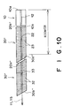
- Fig. 9 is a diagram illustrating the construction of a laser light source as the third embodiment of the present invention.
- Fig. 10 is a diagram illustrating the construction of a laser light source as the fourth embodiment of the present invention.
- Fig. 11 is a diagram illustrating the construction of a laser light source as the fifth embodiment of the present invention.
- Fig. 12 is a diagram illustrating the construction of a laser light source as the sixth embodiment of the present invention.
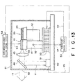
- Fig. 13 is a diagram illustrating an example of an arrangement for use of the laser light source illustrated in Fig. 1.
- Fig. 14 is a diagram illustrating an example of an arrangement for use of the laser light source illustrated in Fig. 6.
- Fig. 15 is a diagram illustrating the construction of an image forming apparatus as the seventh embodiment of the present invention.
- Fig. 16 is a diagram illustrating the construction of an image forming apparatus as the eighth embodiment of the present invention.
- Fig. 17 is a diagram illustrating examples of variation of the optical intensity in the case where a conventional laser light source is used as a recording light source, and is subject to intensity modulation.
- Fig. 18 is a diagram illustrating an example of variation of the optical intensity in the case where a conventional laser light source is used as a recording light source, and is subject to pulse width modulation.
- Fig. 19 is a diagram illustrating a relationship between an optical feedback ratio and a suppression ratio.
- Fig. 1 is a diagram illustrating the construction of a laser light source as the first embodiment of the present invention.
- the laser light source of Fig. 1 comprises a semiconductor laser element (chip) 10 as a semiconductor light-emitting element which emits a laser beam 11, and a waveguide-type wavelength selection element 20 which is butt-coupled to the semiconductor laser element 10 at one end of the semiconductor laser element 10.
- the semiconductor laser element 10 comprises an optical waveguide 12 including an active region.
- An antireflection (AR) coating is provided on an end face lOa of the semiconductor laser element 10, at which the semiconductor laser element 10 is butt-coupled to the waveguide-type wavelength selection element 20.
- the antireflection (AR) coating exhibits a reflectance of 0.5% or less at an oscillation wavelengt ⁇ (which is 950 nm in this example as explained later).
- a low-reflection (LR) coating for the oscillation wavelength ⁇ is provided on the opposite end face 10b of the semiconductor laser element 10.
- the length of the semiconductor laser element 10 is, for example, 1 mm.
- the waveguide-type wavelength selection element 20 is made by forming an optical channel waveguide 22 on a substrate 21, and arranging a DBR (distributed Bragg reflector) grating 23 along the direction of light propagation in the optical channel waveguide 22.
- the substrate 21 is made of, for example, a LiNbO 3 crystal doped with 5 mol% MgO, which is hereinafter called the MgO-LN substrate.
- the grating length is about 1 to 3 mm, and the chip length is also about 1 to 3 mm, so that a reflectance of 90% or more is realized for the oscillation wavelength ⁇ .
- Both end faces 20a and 20b of the waveguide-type wavelength selection element 20, which include end faces of the optical channel waveguide 22, are cut and polished, and antireflection coatings for the oscillation wavelength ⁇ are provided on the polished end faces 20a and 20b.
- the waveguide-type wavelength selection element 20 is formed so that the mode field diameter of the waveguide-type wavelength selection element 20 is almost identical to the mode field diameter of the light emission in the semiconductor laser element 10.
- the semiconductor laser element 10 and the waveguide-type wavelength selection element 20 are arranged so that end faces of the optical waveguide 12 and the optical channel waveguide 22 are opposite each other, and the end face 10a of the semiconductor laser element 10 and the end face 20a of the waveguide-type wavelength selection element 20 are close to each other.
- the distance between the end faces 10a and 20a is 1.5 ⁇ m or less.
- the end face 10a may be in contact with the end face 20a.
- a laser beam 11 having a center wavelength of 950 nm is emitted from the forward-side end face lOb of the semiconductor laser element 10.
- the laser beam 11 is used for a predetermined use such as image formation as explained later.
- Light having a center wavelength of 950 nm is also emitted from the backside end face 10a.
- This light enters and propagates through the optical channel waveguide 22 in the waveguide-type wavelength selection element 20, and a portion of the light is reflected and diffracted by the DBR grating 23, and returns to the semiconductor laser element 10.
- the DBR grating 23 has the function of selecting a wavelength, a wavelength of the above portion of light reflected and diffracted by the DBR grating 23 is selected, and the wavelength-selected light returns to the semiconductor laser element 10. Therefore, the oscillation wavelength of the semiconductor laser element 10 is selected and locked.
- the laser beam 11 having the wavelength of 950 nm is obtained.
- the aforementioned antireflection (AR) coatings are provided on the end face 10a of the semiconductor laser element 10 and the end face 20a of the waveguide-type wavelength selection element 20, substantially, oscillation in a Fabry-Perot mode does not occur either between the opposite end faces 10a and lOb of the semiconductor laser element 10 or between the end face lOb of the semiconductor laser element 10 and the end face 20a of the waveguide-type wavelength selection element 20. That is, in the construction of Fig. 1, a Fabry-Perot type external resonator is realized between the end face lOb of the semiconductor laser element 10 and the DBR grating 23, and the laser beam 11 oscillates substantially only in this external resonator. Therefore, the oscillation wavelength of the laser light source of Fig. 1 is the selected wavelength of the external resonator.
- the laser light source as the first embodiment is used as a recording light source in an image forming apparatus which produces images having density gradation, and the semiconductor laser element 10 is directly modulated, the repeatability of the modulated laser beam is high.
- Fig. 2 is a diagram schematically illustrating a relationship between the driving current and the oscillation wavelength in the conventional laser light source
- Fig. 3 is a diagram schematically illustrating a relationship between the driving current and the oscillation wavelength in the laser light source as the first embodiment, where both the conventional laser light source and the laser light source in the first embodiment comprise a composite resonator formed by a semiconductor laser element and an external resonator.
- the oscillation wavelength varies and hops when the driving current varies, i.e., the mode hopping occurs.
- the oscillation wavelength does not vary, i.e., is maintained constant, even when the driving current varies.
- Fig. 4 is a diagram schematically illustrating a relationship between the driving current and the output power of the conventional laser light source
- Fig. 5 is a diagram schematically illustrating a relationship between the driving current and the output power of the above laser light source as the first embodiment.
- Fig. 4 in the conventional laser light source, a great amount of noise is produced due to the mode hopping caused by the variation of the driving current.
- the laser light source as the first embodiment the noise production is prevented, and linearity is maintained in the relationship between the driving current and the output power of the laser light source, as illustrated in Fig. 5.
- the laser beam 11 exits from the end face 10b, which is located farther from the waveguide-type wavelength selection element 20 than the other end face 10a of the semiconductor laser element 10. Therefore, the internal power of the semiconductor laser element 10 can be lowered, compared with the conventional laser light source in which the laser beam oscillated in the external resonator is output through the wavelength selection element. Consequently, it is possible to prevent the semiconductor laser element 10 from being damaged due to the increase in the internal power.
- the end face 20b of the waveguide-type wavelength selection element 20 is cut at a bevel with respect to the direction of the optical channel waveguide 22. Therefore, light reflected at the end face 20b does not enter the optical channel waveguide 22. Since light reflected at the end face 20b does not return to the semiconductor laser element 10, it is possible to prevent noise production and output variation which will be caused by the returned light.
- the waveguide-type wavelength selection element 20 in the laser light source as the first embodiment is formed by arranging the optical channel waveguide and the DBR grating on the MgO-LN substrate
- other wavelength selection elements can be used.
- the wavelength selection elements which are disclosed in Japanese Patent Applications Nos. 2000-085973 and 2000-085974 can be used.
- the contents of Japanese Patent Applications Nos. 2000-085973 and 2000-085974 are incorporated in this specification by reference.
- These wavelength selection elements are formed by arranging on a substrate made of Si or quartz an optical channel waveguide and a DBR grating which are made of a core material having a refractive index of 1.75 to 2.3.
- Fig. 6 is a diagram illustrating the construction of a laser light source as the second embodiment of the present invention.
- elements having the same reference numbers as Fig. 1 have basically the same functions as the corresponding elements in Fig. 1.
- the laser light source of Fig. 6 is different from the laser light source of Fig. 1 in that the laser light source of Fig. 6 additionally comprises a waveguide-type optical wavelength conversion element 30 which is butt-coupled to the forward-side end face lOb of the semiconductor laser element 10.
- the other construction of the laser light source of Fig. 6 is basically the same as the construction of Fig. 1.
- the optical wavelength conversion element 30 is formed by arranging on a substrate 31 a domain-inverted structure and an optical channel waveguide 33 which extends along the domain-inverted structure.
- the substrate 31 is made of, for example, a LiNbO 3 crystal doped with 5 mol% MgO (hereinafter called a MgO-LN substrate), where LiNbO 3 is a ferroelectric exhibiting a nonlinear effect.
- the domain-inverted structure is formed by periodically arranging a plurality of domain-inverted portions 32. In each of the plurality of domain-inverted portions 32, the direction of the spontaneous polarization, which is originally parallel with the z-axis of the substrate 31, is inverted.
- An antireflection coating for the laser beam 11 (as the fundamental wave) is provided on the polished end face 30a, and another antireflection coating for the laser beam 11 and a second harmonic 15 (which is explained later) is provided on the other polished end face 30b.
- the semiconductor laser element 10 and the optical wavelength conversion element 30 are arranged so that the end faces of the optical waveguide 12 and the optical channel waveguide 33 are opposite each other, and the end faces lOb and 30a are close to each other.
- the distance between the end faces lOb and 30a is 2 ⁇ m or less.
- the end face lOb may be in contact with the end face 30a.
- the laser beam 11 when the laser beam 11 enters the optical wavelength conversion element 30, the laser beam 11 is converted into the second harmonic 15, where the wavelength of the second harmonic 15 is one-half the wavelength of the laser beam 11. Then, both the laser beam 11 and the second harmonic 15 exit from the end face 30b of the optical wavelength conversion element 30.
- an appropriate coating which stops the laser beam 11 is provided on the end face 30b, only the second harmonic 15 exits from the end face 30b.
- the oscillation wavelength of the semiconductor laser element 10 which is selected by the wavelength selection element 20 is 1.02 ⁇ m.
- Antireflection (AR) coatings having a reflectance of 4% at the wavelength of 1.02 ⁇ m are provided on the end face 10a of the semiconductor laser element 10 and the end face 20a of the waveguide-type wavelength selection element 20.
- the distance between the end face 10a of the semiconductor laser element 10 and the end face 20a of the waveguide-type wavelength selection element 20 is 1.5 ⁇ m, which is approximately a half-integer multiple of the above selected wavelength. Therefore, light reflected at the end face 10a and light reflected at the end face 20a interfere with each other so as to cancel each other out. That is, the effect of reducing the reflected light is enhanced.
- antireflection (AR) coatings are provided on the end face lOa of the semiconductor laser element 10 and the end face 20a of the waveguide-type wavelength selection element 20, as above.
- AR antireflection
- the distance between the end face 10a of the semiconductor laser element 10 and the end face 20a of the waveguide-type wavelength selection element 20 varies due to deviations which occur when the semiconductor laser element 10 and the waveguide-type wavelength selection element 20 are aligned and fixed.
- the variation of the distance is usually about 0.2 ⁇ m.
- the oscillation wavelengt ⁇ is about 1 ⁇ m, the above variation of the distance nearly equals ⁇ /4.
- antireflection coatings which realize a reflectance of 0.1% on the end faces, such antireflection coatings are expensive.
- antireflection coatings which realize a reflectance of 0.1 to 0.8% are provided on the end faces 10a and 20a, and the distance between the end faces 10a and 20a is fixed to a half-integer multiple of the selected wavelength ⁇ with a precision of ⁇ /4.
- the substantial reflectance of the antireflection optical system can be made 0.5% or less.
- the laser beam 11 oscillates substantially only in an external resonator formed between the forward end face 10b of the semiconductor laser element 10 and the DBR grating 23. Therefore, the laser light source as the second embodiment of the present invention also has the same advantages as the first embodiment.
- the output power of the second harmonic is proportional to the square of the output power of the fundamental wave
- the variation of the output power of the second harmonic becomes great when the mode hopping occurs, and repeatability of the driving current-second harmonic output characteristic of the laser light source is further lowered due to the mode hopping.
- the variation of the oscillation wavelength and the mode hopping can be suppressed. Therefore, the variation of the second harmonic 15 can be effectively prevented in the second embodiment of the present invention.
- Fig. 7 is a diagram schematically illustrating a relationship between the driving current and the output power of the second harmonic in a conventional laser light source
- Fig. 8 is a diagram schematically illustrating a relationship between the driving current and the output power of the second harmonic in the laser light source as the second embodiment of the present invention, where both of the conventional laser light source and the laser light source in the second embodiment comprise an optical wavelength conversion element and a composite resonator formed by a semiconductor laser element and an external resonator.
- both of the conventional laser light source and the laser light source in the second embodiment comprise an optical wavelength conversion element and a composite resonator formed by a semiconductor laser element and an external resonator.
- the end face 30b of the optical wavelength conversion element 30 is cut at a bevel with respect to the direction of the optical channel waveguide 33. Therefore, light reflected at the end face 30b does not enter the optical channel waveguide 33 of the optical wavelength conversion element 30. Consequently, the above light reflected at the end face 30b does not return to the semiconductor laser element 10. Thus, it is possible to prevent noise production and output variation which may be caused by the returned light.
- Fig. 9 is a diagram illustrating the construction of a laser light source as the third embodiment of the present invention.
- elements having the same reference numbers as Fig. 6 have basically the same functions as the corresponding elements in Fig. 6.
- the laser light source of Fig. 9 is different from the laser light source of Fig. 6 in that the waveguide-type wavelength selection element 20' is arranged between the semiconductor laser element 10 and the optical wavelength conversion element 30', instead of being arranged on the backside of the semiconductor laser element 10.
- the waveguide-type wavelength selection element 20' is butt-coupled to each of the semiconductor laser element 10 and the optical wavelength conversion element 30'.
- a portion of light which exits from the forward-side end face lOb of the semiconductor laser element 10 is reflected and diffracted by the DBR grating 23 in the waveguide-type wavelength selection element 20', and returns to the semiconductor laser element 10. Since the DBR grating 23 has the function of selecting a wavelength, the wavelength of the reflected and diffracted portion of light is selected, and the wavelength-selected light returns to the semiconductor laser element 10. Therefore, the oscillation wavelength of the semiconductor laser element 10 is selected and locked.
- Fabry-Perot mode does not occur either between the opposite end faces 10a and 10b of the semiconductor laser element 10 or between the end face 10a of the semiconductor laser element 10 and the end face 20b' of the waveguide-type wavelength selection element 20'. That is, in the construction of Fig. 9, a Fabry-Perot type external resonator is realized between the end face 10a of the semiconductor laser element 10 and the DBR grating 23, and the laser beam 11 oscillates substantially only in this external resonator.
- the oscillation wavelength of the laser light source of Fig. 9 is the selected wavelength of the external resonator.
- the oscillation wavelength does not vary. Consequently, the mode hopping does not occur even when the driving current varies, and noise production due to the mode hopping can be prevented.
- the variation of the oscillation wavelength and the mode hopping can also be suppressed in the third embodiment, the variation of the output power of the second harmonic due to the mode hopping can be surely suppressed, and the lowering of repeatability of the driving current-second harmonic output characteristic of the laser light source can be prevented.
- Fig. 10 is a diagram illustrating the construction of a laser light source as the fourth embodiment of the present invention.
- elements having the same reference numbers as Fig. 9 have basically the same functions as the corresponding elements in Fig. 9.
- the laser light source of Fig. 10 is different from the laser light source of Fig. 9 in that the end face 20a" of the waveguide-type wavelength selection element 20" and the end faces 30a" and 30b" of the optical wavelength conversion element 30" are cut at a bevel with respect to the direction in which the optical waveguides 22 and 33 extend. Therefore, light reflected at the end face 20a", 30a", or 30b" does not return to the semiconductor laser element 10. Consequently, it is possible to prevent noise production and output variation which may be caused by the returned light.
- Fig. 11 is a diagram illustrating the construction of a laser light source as the fifth embodiment of the present invention.
- elements having the same reference numbers as Fig. 9 have basically the same functions as the corresponding elements in Fig. 9.
- the laser light source of Fig. 11 is different from the laser light source of Fig. 9 in that the optical wavelength conversion element 30' is arranged between the semiconductor laser element 10' and the waveguide-type wavelength selection element 20'.
- the optical wavelength conversion element 30' is butt-coupled to each of the semiconductor laser element 10' and the waveguide-type wavelength selection element 20'.
- a high-reflection (HR) coating for the wavelength of the laser beam 11 is provided on an end face 10a' of the semiconductor laser element 10'.
- An antireflection (AR) coating for the wavelength is provided on the opposite end face 10b of the semiconductor laser element 10', at which the semiconductor laser element 10' is butt-coupled to the optical wavelength conversion element 30'.
- Antireflection (AR) coatings are provided on both end faces 30a and 30b' of the optical wavelength conversion element 30' and both end faces 20a and 20b' of the waveguide-type wavelength selection element 20'.
- an external resonator in which light having the wavelength selected by the waveguide-type wavelength selection element 20' oscillates is formed between the end face 10a' of the semiconductor laser element 10' and the waveguide-type wavelength selection element 20', and the laser beam 11 generated in the external resonator is converted into the second harmonic 15 by the optical wavelength conversion element 30'.
- the efficiency of diffraction and reflection of the light having the selected wavelength in the waveguide-type wavelength selection element 20' it is preferable to enhance the efficiency of diffraction and reflection of the light having the selected wavelength in the waveguide-type wavelength selection element 20'.
- the efficiency is enhanced, the internal power of the external resonator can be increased. Therefore, it is possible to obtain the second harmonic 15 with greater output power.
- Fig. 12 is a diagram illustrating the construction of a laser light source as the sixth embodiment of the present invention.
- elements having the same reference numbers as Fig. 11 have basically the same functions as the corresponding elements in Fig. 11.
- the laser light source of Fig. 12 is different from the laser light source of Fig. 11 in the relative positions of the waveguide-type wavelength selection element 20' and the optical wavelength conversion element 30'. That is, the waveguide-type wavelength selection element 20' is arranged between the semiconductor laser element 10' and the optical wavelength conversion element 30'.
- the end faces of the semiconductor laser element 10', the waveguide-type wavelength selection element 20', and the optical wavelength conversion element 30' are coated in the same manners as the fifth embodiment. Therefore, in the construction of Fig.
- the laser light source of Fig. 12 has substantially the same advantages as those of the laser light source of Fig. 11.
- Fig. 13 is a diagram illustrating an example of an arrangement for use of the laser light source of Fig. 1.
- the semiconductor laser element (chip) 10 and the waveguide-type wavelength selection element 20 of the laser light source are held in the blocks 41 and 42, respectively.
- the blocks 41 and 42 are made of a metal having a high thermal conductivity, such as copper.
- the metal block 42 is fixed to the metal block 41, and the metal block 41 is fixed on an upper surface (as a temperature control surface) of a Peltier element 50.
- the arrangement of Fig. 13 further includes a collimator lens 45, a beam splitter 46, and a photodetector 51.
- the collimator lens 45 collimates the laser beam 11 which is emitted from the semiconductor laser element 10 as divergent light. A portion of the collimated laser beam is branched off by the beam splitter 46, and directed to the photodetector 51.
- the photodetector 51 is, for example, a photodiode, and detects the intensity of the laser beam 11.
- the above construction is contained in a package comprised of a package base 60 and a package cover 61 which covers the package base 60.
- the package cover 61 has a window 62 made of glass.
- the laser beam 11 which passes through the beam splitter 46 exits from the package through the glass window 62, and is used for a predetermined purpose.
- a thermistor 52 is provided for detecting the ambient temperature of the external resonator formed between the end face 10b of the semiconductor laser element 10 and the DBR grating 23.
- the thermistor 52 outputs a temperature detection signal S1, which is then input into a temperature control circuit 53.
- the temperature control circuit 53 supplies to the Peltier element 50 a Peltier-element driving control signal S2 corresponding to the temperature detection signal S1 so as to control the Peltier element 50.
- the photodetector 51 outputs an optical-intensity detection signal S3, which is fed back to a semiconductor laser driving control circuit 54.
- the semiconductor-laser driving control circuit 54 varies a driving current S4 which is supplied to the semiconductor laser element 10, based on the optical-intensity detection signal S3, so as to maintain the optical output (of the laser beam 11) at a predetermined level.
- Fig. 14 is a diagram illustrating an example of an arrangement for use of the laser light source illustrated in Fig. 6.
- the semiconductor laser element (chip) 10 the waveguide-type wavelength selection element 20, and the optical wavelength conversion element 30 of the laser light source are held in the blocks 41, 42, and 43, respectively.
- the blocks 41, 42, and 43 are made of a metal having a high thermal conductivity, such as copper.
- the metal blocks 41 and 42 are fixed to the metal block 43, and the metal block 43 is fixed on an upper surface (as a temperature control surface) of a Peltier element 50.
- the laser beam 11 (as the fundamental wave) and its second harmonic 15 exit from the end face 30b of the optical wavelength conversion element 30, the laser beam 11 is cut off by a fundamental-wave cut filter 47, which is arranged between the collimator lens 45 and the beam splitter 46 in the construction of Fig. 14. Therefore, in this case, the photodetector 51 detects the optical intensity of a portion of the second harmonic 15 which is branched off by the beam splitter 46, and the semiconductor laser element 10 is controlled by the semiconductor-laser driving control circuit 54 so that the optical intensity of the second harmonic 15 is maintained at a predetermined level.
- Fig. 15 is a diagram illustrating the construction of an image forming apparatus as the seventh embodiment of the present invention.
- the image forming apparatus of Fig. 15 is provided for forming a color image on a recording medium 80.
- the image forming apparatus of Fig. 15 comprises three laser light sources 71, 72, and 73, cylindrical lenses 74, 75, and 76, a polygon mirror 77, and another cylindrical lens 78, and an f-theta lens 79.
- the cylindrical lenses 74, 75, and 76 respectively converge laser beams 81, 82, and 83, which are emitted from the laser light sources 71, 72, and 73 for recording the color image, into the plane of Fig. 15.
- the laser beams 81, 82, and 83 are called the recording laser beams.
- the polygon mirror 77 is arranged so that the recording laser beams 81, 82, and 83 are respectively converged by the cylindrical lenses 74, 75, and 76, into a common converging position on a mirror face of the polygon mirror 77.
- the polygon mirror 77 reflects the converged recording laser beams 81, 82, and 83 so as to be deflected toward the cylindrical lens 78.
- the cylindrical lenses 74, 75, 76, and 78 constitute a face-inclination-correction optical system.
- the f-theta lens 79 converges the deflected recording laser beams 81, 82, and 83 into a predetermined spot having a predetermined diameter, regardless of deflected position on the recording medium 80.
- each of the above laser light sources 71, 72, and 73 has the construction of Fig. 13.
- the oscillation wavelengths ⁇ 1, ⁇ 2, and ⁇ 3 of the laser light sources 71, 72, and 73 are different, and respectively used for forming blue, green, and red on the recording medium 80.
- a modulation circuit, a semiconductor laser driving circuit, and a temperature control circuit are provided corresponding to each of the laser light sources 71, 72, and 73, and image data corresponding to each color component of a color image are supplied from an image data source 93 to each modulation circuit.
- the modulation circuit 84 when image data DB indicating the blue density are supplied to the modulation circuit 84, the modulation circuit 84 generates a modulation signal MB based on the image data DB, and outputs the modulation signal MB to the semiconductor laser driving circuit 85, which controls a driving current which is supplied to the corresponding laser light source 71, based on the modulation signal MB.
- the temperature regulator 86 is provided for maintaining the temperature of the resonator portion of the laser light source 71 at a predetermined target temperature.
- the semiconductor laser driving circuit 85 may be: a type which controls based on the modulation signal MB the level of the driving current supplied to the corresponding laser light source 71; a type which controls based on the modulation signal MB a pulse width of a pulsed driving current supplied to the corresponding laser light source 71; a type which controls based on the modulation signal MB the number of pulses of a pulsed driving current supplied to the corresponding laser light source 71; or the like.
- the semiconductor laser driving circuit 85 When the semiconductor laser driving circuit 85 is the type which controls based on the modulation signal MB the level of the driving current supplied to the corresponding laser light source 71, the recording laser beam 81 is intensity-modulated based on the modulation signal MB.
- the level of the driving current can be controlled, for example, by using the photodetector 51 and the semiconductor-laser driving control circuit 54 which are illustrated in Fig. 13.
- the semiconductor-laser driving control circuit 54 (in Fig. 13) may controls the driving current S4 which is supplied to the semiconductor laser element 10 the so that the optical intensity of the recording laser beam 81 becomes the intensity-modulated level corresponding to the modulation signal MB.
- the driving current may be controlled based on a relationship between the driving current and the optical intensity of the recording laser beam 81, which is obtained in advance by measurement.
- the relationship can be obtained by measuring the optical intensity when the image forming apparatus is in a quiescent state.
- a monitoring means such as the photodetector 51 can be used in the measurement, and appropriate values of the driving current, corresponding to respective values of the optical intensity, can be held for use in the control of the level of the driving current during operation.
- the semiconductor laser driving circuit 85 When the semiconductor laser driving circuit 85 is the type which controls based on the modulation signal MB a pulse width of a pulsed driving current supplied to the corresponding laser light source 71, the recording laser beam 81 is pulse-width modulated based on the image data DB.
- the values of the pulse width of the driving current, corresponding to respective levels of the modulation signal MB can be obtained in advance based on a relationship between the driving current and the optical intensity of the recording laser beam 81, and held for use in the control of the pulse width of the driving current during operation.
- the relationship between the driving current and the optical intensity of the recording laser beam 81 is obtained by measurement, which is performed when the image forming apparatus is in a quiescent state.
- a monitoring means such as the photodetector 51 can be used in the measurement.
- the temperature regulator 86 is realized, for example, by the thermistor 52, the temperature control circuit 53, and the Peltier element 50 in the construction of Fig. 13.
- the modulation circuit 87 when image data DG indicating the green density are supplied to the modulation circuit 87, the modulation circuit 87 generates a modulation signal MG based on the image data DG, and outputs the modulation signal MG to the semiconductor laser driving circuit 88, which controls a driving current which is supplied to the corresponding laser light source 72, based on the modulation signal MG.
- the temperature regulator 89 is provided for maintaining the temperature of the resonator portion of the laser light source 72 at a predetermined target temperature.
- the modulation circuit 87, the semiconductor laser driving circuit 88, and the temperature control circuit 89 are realized in the same manners as the modulation circuit 84, the semiconductor laser driving circuit 85, and the temperature control circuit 86, respectively.
- the modulation circuit 90 when image data DR indicating the red density are supplied to the modulation circuit 90, the modulation circuit 90 generates a modulation signal MR based on the image data DR, and outputs the modulation signal MR to the semiconductor laser driving circuit 91, which controls a driving current which is supplied to the corresponding laser light source 73, based on the modulation signal MR.
- the temperature regulator 92 is provided for maintaining the temperature of the resonator portion of the laser light source 73 at a predetermined target temperature.
- the modulation circuit 90, the semiconductor laser driving circuit 91, and the temperature control circuit 92 are realized in the same manners as the modulation circuit 84, the semiconductor laser driving circuit 85, and the temperature control circuit 86, respectively.
- the recording laser beams 81, 82, and 83 being emitted from the laser light sources 71, 72, and 73 and having the different wavelengths are reflected and deflected by the polygon mirror 77 so as to scan the recording medium 80 in the X direction (i.e., the main scanning direction).
- the recording medium 80 is moved by a sub-scanning (feeding) means (not shown) at a constant speed in the Y direction, which is approximately perpendicular to the X direction.
- the recording medium 80 is two-dimensionally scanned with the recording laser beams 81, 82, and 83.
- the recording medium 80 includes color-forming layers for forming blue, green, and red, respectively.
- the recording medium 80 is illuminated with the recording laser beams 81, 82, and 83 having the wavelengths ⁇ 1, ⁇ 2, and ⁇ 3, the color-forming layers form blue, green, and red images, respectively.
- the color-forming layers included in the recording medium 80 form blue, green, and red with densities corresponding to the image data DB, DG, and DR, respectively, so as to form (record) a color image represented by the image data DB, DG, and DR on the recording medium 80 when the recording medium 80 is two-dimensionally scanned with the recording laser beams 81, 82, and 83.
- the wavelengths ⁇ 1, ⁇ 2, and ⁇ 3 do not belong to the blue, green, and red wavelength ranges, respectively. In this case, a so-called pseudo color image is formed.
- the laser light sources 71, 72, and 73 have basically the same construction as the construction of Fig. 13. Therefore, the oscillation wavelength in each laser light source does not vary even when the optical length of the semiconductor laser element in each laser light source varies due to variation of the driving current injected into the semiconductor laser element. Consequently, the mode hopping due to the variation of the driving current does not occur, and noise production caused by the mode hopping can be prevented. Thus, in the image forming apparatus of Fig. 15, the noise production caused by the mode hopping can be prevented even when the recording laser beams 81, 82, and 83 are intensity-modulated, pulse-width modulated, or pulse-number modulated, and therefore high-quality color images can be formed on the recording medium 80. In addition, since the repeatability of the modulated laser beams, which are obtained when the laser light sources 71, 72, and 73 are modulated, is high, the repeatability of the image density is also maintained high.
- the recording medium 80 may be a type which forms blue, green, and red images when the recording medium 80 is illuminated with the recording laser beams 81, 82, and 83, and then undergoes a wet or dry developing process.
- the above recording medium 80 used in the seventh embodiment is a positive type
- a negative-type recording medium in which a negative image is formed may be used instead of the positive-type recording medium 80.
- a positive image can be produced in a positive-type recording medium by using the negative image which is formed in the negative-type recording medium by illumination with the recording laser beams 81, 82, and 83.
- Fig. 16 is a diagram illustrating the construction of an image forming apparatus as the eighth embodiment of the present invention.
- the image forming apparatus of Fig. 16 is different from the image forming apparatus of Fig. 15 in that the recording medium 80' includes color-forming layers which respectively form colors of yellow, magenta, and cyan when the recording medium 80' is illuminated with the recording laser beams 111, 112, and 113 respectively having wavelengths in the blue, green, and red wavelength ranges.
- the laser light source 101 has, for example, the construction of Fig. 14, in which a laser beam as a fundamental wave is converted by an optical wavelength conversion element into the laser beam 111 (which is a second harmonic) having a wavelength in the blue wavelength range.
- the laser light source 102 has, for example, the construction of Fig. 14, in which a laser beam as a fundamental wave is converted by an optical wavelength conversion element into the laser beam 112 (which is a second harmonic) having a wavelength in the green wavelength range.
- the laser light source 103 has, for example, the construction of Fig. 13, and emits the laser beam 113 having a wavelength in the red wavelength range.
- the recording laser beams 111, 112, and 113 are modulated, and the recording medium 80' is two-dimensionally scanned with the modulated recording laser beams 111, 112, and 113 so that a color image is formed in the recording medium 80'.
- the oscillation wavelength in each laser light source does not vary even when the optical length of the semiconductor laser element in each laser light source varies due to variation of the driving current injected into the semiconductor laser element. Therefore, the mode hopping due to the variation of the driving current does not occur, and noise production caused by the mode hopping can be prevented. Consequently, in the image forming apparatus of Fig. 16, the noise production caused by the mode hopping can be prevented even when the recording laser beams 111, 112, and 113 are intensity-modulated, pulse-width modulated, or pulse-number modulated, and therefore high-quality color images can be formed on the recording medium 80'. In addition, since the repeatability of the modulated laser beams, which are obtained when the laser light sources 101, 102, and 103 are modulated, is high, the repeatability of the image density is also maintained high.
Applications Claiming Priority (8)
| Application Number | Priority Date | Filing Date | Title |
|---|---|---|---|
| JP34572499 | 1999-12-06 | ||
| JP34572499 | 1999-12-06 | ||
| JP2000157792 | 2000-05-29 | ||
| JP2000157792 | 2000-05-29 | ||
| JP2000196166 | 2000-06-29 | ||
| JP2000196166 | 2000-06-29 | ||
| JP2000326383 | 2000-10-26 | ||
| JP2000326383 | 2000-10-26 |
Publications (2)
| Publication Number | Publication Date |
|---|---|
| EP1130717A2 true EP1130717A2 (fr) | 2001-09-05 |
| EP1130717A3 EP1130717A3 (fr) | 2003-03-19 |
Family
ID=27480662
Family Applications (1)
| Application Number | Title | Priority Date | Filing Date |
|---|---|---|---|
| EP00126707A Withdrawn EP1130717A3 (fr) | 1999-12-06 | 2000-12-05 | Source laser à semiconducteur à cavité externe |
Country Status (2)
| Country | Link |
|---|---|
| US (1) | US20010050932A1 (fr) |
| EP (1) | EP1130717A3 (fr) |
Cited By (7)
| Publication number | Priority date | Publication date | Assignee | Title |
|---|---|---|---|---|
| EP1313186A1 (fr) * | 2001-11-19 | 2003-05-21 | Agilent Technologies, Inc. (a Delaware corporation) | Laser stabilisée par un réseau sur une fibre |
| WO2005104316A1 (fr) * | 2004-04-27 | 2005-11-03 | Bookham Technology Plc | Source laser stabilisee a retroaction relative tres elevee et faible large de bande |
| EP1609221A2 (fr) * | 2003-03-19 | 2005-12-28 | Binoptics Corporation | Lasers mordances unidirectionnels a fort smsr, et dispositif photonique a faible retroreflexion |
| WO2007065455A1 (fr) * | 2005-12-06 | 2007-06-14 | Pirelli & C. S.P.A. | Commande de phase passive dans un laser a cavite externe |
| US8259765B2 (en) | 2006-12-06 | 2012-09-04 | Google Inc. | Passive phase control in an external cavity laser |
| US8526103B2 (en) | 2010-01-08 | 2013-09-03 | Oclaro Technology Limited | Laser system with highly linear output |
| US10541509B2 (en) | 2016-01-28 | 2020-01-21 | Sony Corporation | Semiconductor light emitting device |
Families Citing this family (5)
| Publication number | Priority date | Publication date | Assignee | Title |
|---|---|---|---|---|
| JP2002176224A (ja) * | 2000-12-07 | 2002-06-21 | Fuji Photo Film Co Ltd | レーザー光源 |
| JP4841428B2 (ja) * | 2004-02-27 | 2011-12-21 | パナソニック株式会社 | 映像投射装置 |
| JP2005354032A (ja) * | 2004-05-12 | 2005-12-22 | Canon Inc | 分布ブラッグ反射型半導体レーザの制御方法および画像投影装置 |
| JPWO2007026510A1 (ja) * | 2005-08-29 | 2009-03-26 | パナソニック株式会社 | ファイバレーザおよび光学装置 |
| DE102022115317A1 (de) | 2022-06-20 | 2023-12-21 | Trumpf Laser Gmbh | Laservorrichtung |
Citations (8)
| Publication number | Priority date | Publication date | Assignee | Title |
|---|---|---|---|---|
| JPH0373583A (ja) * | 1989-08-14 | 1991-03-28 | Nippon Telegr & Teleph Corp <Ntt> | 半導体レーザ光源装置 |
| EP0592226A1 (fr) * | 1992-10-07 | 1994-04-13 | Matsushita Electric Industrial Co., Ltd. | Dispositif de conversion de longeur d'onde optique |
| US5440352A (en) * | 1993-03-04 | 1995-08-08 | Schneider Rundfunkwerke Aktiengesellschaft | Laser-driven television projection system with attendant color correction |
| WO1995024618A2 (fr) * | 1994-03-11 | 1995-09-14 | Philips Electronics N.V. | Dispositif servant a augmenter la frequence d'un rayonnement electromagnetique |
| US5499256A (en) * | 1995-02-14 | 1996-03-12 | Deacon Research | Polarized frequency-selective optical source |
| US5513196A (en) * | 1995-02-14 | 1996-04-30 | Deacon Research | Optical source with mode reshaping |
| WO1996018132A1 (fr) * | 1994-12-07 | 1996-06-13 | Fredrik Laurell | Dispositif laser a diode a frequence doublee |
| US5699377A (en) * | 1996-04-30 | 1997-12-16 | E-Tek Dynamics, Inc. | Narrow linewidth, stabilized semiconductor laser source |
Family Cites Families (4)
| Publication number | Priority date | Publication date | Assignee | Title |
|---|---|---|---|---|
| US5682398A (en) * | 1996-05-03 | 1997-10-28 | Eastman Kodak Company | Frequency conversion laser devices |
| JP3006832B2 (ja) * | 1996-05-14 | 2000-02-07 | 日本電気株式会社 | 発光素子と光導波路の光結合構造 |
| JPH10221572A (ja) * | 1997-02-07 | 1998-08-21 | Fujitsu Ltd | 光装置 |
| US6363097B1 (en) * | 1998-09-18 | 2002-03-26 | Nec Corporation | Semiconductor laser with a rewritable wavelength stabilizer |
-
2000
- 2000-12-05 EP EP00126707A patent/EP1130717A3/fr not_active Withdrawn
- 2000-12-05 US US09/730,248 patent/US20010050932A1/en not_active Abandoned
Patent Citations (8)
| Publication number | Priority date | Publication date | Assignee | Title |
|---|---|---|---|---|
| JPH0373583A (ja) * | 1989-08-14 | 1991-03-28 | Nippon Telegr & Teleph Corp <Ntt> | 半導体レーザ光源装置 |
| EP0592226A1 (fr) * | 1992-10-07 | 1994-04-13 | Matsushita Electric Industrial Co., Ltd. | Dispositif de conversion de longeur d'onde optique |
| US5440352A (en) * | 1993-03-04 | 1995-08-08 | Schneider Rundfunkwerke Aktiengesellschaft | Laser-driven television projection system with attendant color correction |
| WO1995024618A2 (fr) * | 1994-03-11 | 1995-09-14 | Philips Electronics N.V. | Dispositif servant a augmenter la frequence d'un rayonnement electromagnetique |
| WO1996018132A1 (fr) * | 1994-12-07 | 1996-06-13 | Fredrik Laurell | Dispositif laser a diode a frequence doublee |
| US5499256A (en) * | 1995-02-14 | 1996-03-12 | Deacon Research | Polarized frequency-selective optical source |
| US5513196A (en) * | 1995-02-14 | 1996-04-30 | Deacon Research | Optical source with mode reshaping |
| US5699377A (en) * | 1996-04-30 | 1997-12-16 | E-Tek Dynamics, Inc. | Narrow linewidth, stabilized semiconductor laser source |
Non-Patent Citations (1)
| Title |
|---|
| PATENT ABSTRACTS OF JAPAN vol. 015, no. 240 (E-1079), 20 June 1991 (1991-06-20) -& JP 03 073583 A (NIPPON TELEGR & TELEPH CORP), 28 March 1991 (1991-03-28) * |
Cited By (9)
| Publication number | Priority date | Publication date | Assignee | Title |
|---|---|---|---|---|
| EP1313186A1 (fr) * | 2001-11-19 | 2003-05-21 | Agilent Technologies, Inc. (a Delaware corporation) | Laser stabilisée par un réseau sur une fibre |
| EP1609221A2 (fr) * | 2003-03-19 | 2005-12-28 | Binoptics Corporation | Lasers mordances unidirectionnels a fort smsr, et dispositif photonique a faible retroreflexion |
| EP1609221A4 (fr) * | 2003-03-19 | 2006-05-24 | Binoptics Corp | Lasers mordances unidirectionnels a fort smsr, et dispositif photonique a faible retroreflexion |
| US10063028B2 (en) | 2003-03-19 | 2018-08-28 | Macom Technology Solutions Holdings, Inc. | High SMSR unidirectional etched lasers and low back-reflection photonic device |
| WO2005104316A1 (fr) * | 2004-04-27 | 2005-11-03 | Bookham Technology Plc | Source laser stabilisee a retroaction relative tres elevee et faible large de bande |
| WO2007065455A1 (fr) * | 2005-12-06 | 2007-06-14 | Pirelli & C. S.P.A. | Commande de phase passive dans un laser a cavite externe |
| US8259765B2 (en) | 2006-12-06 | 2012-09-04 | Google Inc. | Passive phase control in an external cavity laser |
| US8526103B2 (en) | 2010-01-08 | 2013-09-03 | Oclaro Technology Limited | Laser system with highly linear output |
| US10541509B2 (en) | 2016-01-28 | 2020-01-21 | Sony Corporation | Semiconductor light emitting device |
Also Published As
| Publication number | Publication date |
|---|---|
| US20010050932A1 (en) | 2001-12-13 |
| EP1130717A3 (fr) | 2003-03-19 |
Similar Documents
| Publication | Publication Date | Title |
|---|---|---|
| US4786132A (en) | Hybrid distributed bragg reflector laser | |
| US7463664B2 (en) | Coherent light source and optical device | |
| EP0169567B1 (fr) | Dispositif laser à semi-conducteur | |
| JP5206187B2 (ja) | 光半導体装置 | |
| EP1840638B1 (fr) | Source de lumiere ayant une fonction de modulation, et procede de modulation de la lumiere | |
| US20020015433A1 (en) | Tunable frequency stabilized fiber grating laser | |
| US6839376B2 (en) | Laser light source | |
| EP1130717A2 (fr) | Source laser à semiconducteur à cavité externe | |
| JP2001320124A (ja) | 変調器集積化光源及び光通信用モジュール | |
| EP1691458B1 (fr) | Laser a semi-conducteur de type resonateur externe | |
| US6711183B1 (en) | Optical wavelength conversion device, coherent light generator, and optical information processing apparatus | |
| US20030012246A1 (en) | Semiconductor zigzag laser and optical amplifier | |
| US6944194B1 (en) | Light scanning and recording apparatus | |
| US6273620B1 (en) | Semiconductor light emitting module | |
| KR950015079B1 (ko) | 광 통신 레이저 | |
| US6524016B1 (en) | Semiconductor laser module | |
| JP2011086714A (ja) | 波長可変レーザ | |
| JP2002204025A (ja) | レーザー光源および画像形成装置 | |
| JP3382471B2 (ja) | 半導体光デバイス及びそれを用いた光ネットワーク | |
| US11754907B2 (en) | Photon-pair source for quantum applications | |
| JPS6250075B2 (fr) | ||
| JPH0311554B2 (fr) | ||
| JPS61290787A (ja) | 半導体レ−ザ装置 | |
| US20100254422A1 (en) | Semiconductor laser | |
| Bergonzo et al. | Tuning range extension by active mode-locking of external cavity laser including a linearly chirped fiber Bragg grating |
Legal Events
| Date | Code | Title | Description |
|---|---|---|---|
| PUAI | Public reference made under article 153(3) epc to a published international application that has entered the european phase |
Free format text: ORIGINAL CODE: 0009012 |
|
| AK | Designated contracting states |
Kind code of ref document: A2 Designated state(s): AT BE CH CY DE DK ES FI FR GB GR IE IT LI LU MC NL PT SE TR |
|
| AX | Request for extension of the european patent |
Free format text: AL;LT;LV;MK;RO;SI |
|
| PUAL | Search report despatched |
Free format text: ORIGINAL CODE: 0009013 |
|
| AK | Designated contracting states |
Kind code of ref document: A3 Designated state(s): AT BE CH CY DE DK ES FI FR GB GR IE IT LI LU MC NL PT SE TR Designated state(s): AT BE CH CY DE DK ES FI FR GB GR IE IT LI LU MC NL PT SE TR |
|
| AX | Request for extension of the european patent |
Extension state: AL LT LV MK RO SI |
|
| 17P | Request for examination filed |
Effective date: 20030521 |
|
| 17Q | First examination report despatched |
Effective date: 20030916 |
|
| AKX | Designation fees paid |
Designated state(s): DE FR GB NL |
|
| STAA | Information on the status of an ep patent application or granted ep patent |
Free format text: STATUS: THE APPLICATION IS DEEMED TO BE WITHDRAWN |
|
| 18D | Application deemed to be withdrawn |
Effective date: 20040127 |