EP1120840A2 - Organic luminescence device - Google Patents
Organic luminescence device Download PDFInfo
- Publication number
- EP1120840A2 EP1120840A2 EP01300728A EP01300728A EP1120840A2 EP 1120840 A2 EP1120840 A2 EP 1120840A2 EP 01300728 A EP01300728 A EP 01300728A EP 01300728 A EP01300728 A EP 01300728A EP 1120840 A2 EP1120840 A2 EP 1120840A2
- Authority
- EP
- European Patent Office
- Prior art keywords
- substituted
- group
- organic
- unsubstituted
- layer
- Prior art date
- Legal status (The legal status is an assumption and is not a legal conclusion. Google has not performed a legal analysis and makes no representation as to the accuracy of the status listed.)
- Withdrawn
Links
- 0 CC(*)C1(CC(C)CC2C3(C(CC(C)CC(C)(C4)C5=CCCCC5)C4C4C3CC(C)CC(C)(CC3CC(C5)C5CC3)C4)C(CC(C)CC(CCC(CC3)C3N)(C3)C4CCCC4)C3C2C1)C1[C@@]2C1CCC2 Chemical compound CC(*)C1(CC(C)CC2C3(C(CC(C)CC(C)(C4)C5=CCCCC5)C4C4C3CC(C)CC(C)(CC3CC(C5)C5CC3)C4)C(CC(C)CC(CCC(CC3)C3N)(C3)C4CCCC4)C3C2C1)C1[C@@]2C1CCC2 0.000 description 10
- YXFVVABEGXRONW-UHFFFAOYSA-N Cc1ccccc1 Chemical compound Cc1ccccc1 YXFVVABEGXRONW-UHFFFAOYSA-N 0.000 description 3
- IVSZLXZYQVIEFR-UHFFFAOYSA-N Cc1cccc(C)c1 Chemical compound Cc1cccc(C)c1 IVSZLXZYQVIEFR-UHFFFAOYSA-N 0.000 description 2
- NDVXSCDMBHGYKQ-UUILKARUSA-N C/C=C/c1ccc(C([Si](C)(C)C(c2ccc[s]2)=C2c3ccccc3)=C2c2ccccc2)[s]1 Chemical compound C/C=C/c1ccc(C([Si](C)(C)C(c2ccc[s]2)=C2c3ccccc3)=C2c2ccccc2)[s]1 NDVXSCDMBHGYKQ-UUILKARUSA-N 0.000 description 1
- OLEMFCJPUIFOAY-UHFFFAOYSA-N CC1(C)c(cc(cc2)N3Cc4cc(C)ccc4-c4ccccc4C3)c2-c(cc2)c1cc2N(c1ccccc1)c1cc(C)ccc1 Chemical compound CC1(C)c(cc(cc2)N3Cc4cc(C)ccc4-c4ccccc4C3)c2-c(cc2)c1cc2N(c1ccccc1)c1cc(C)ccc1 OLEMFCJPUIFOAY-UHFFFAOYSA-N 0.000 description 1
- ABMKWMASVFVTMD-UHFFFAOYSA-N Cc(cccc1)c1-c1c(C)cccc1 Chemical compound Cc(cccc1)c1-c1c(C)cccc1 ABMKWMASVFVTMD-UHFFFAOYSA-N 0.000 description 1
- DKFYQMSLASQUNW-UHFFFAOYSA-N Cc1ccc(C2(CCCCC2)c(cc2)ccc2N)cc1 Chemical compound Cc1ccc(C2(CCCCC2)c(cc2)ccc2N)cc1 DKFYQMSLASQUNW-UHFFFAOYSA-N 0.000 description 1
- JJYPMNFTHPTTDI-UHFFFAOYSA-N Cc1cccc(N)c1 Chemical compound Cc1cccc(N)c1 JJYPMNFTHPTTDI-UHFFFAOYSA-N 0.000 description 1
- HMZHPDZCVINDPO-UHFFFAOYSA-N N=C1CCCC1 Chemical compound N=C1CCCC1 HMZHPDZCVINDPO-UHFFFAOYSA-N 0.000 description 1
- PAYRUJLWNCNPSJ-UHFFFAOYSA-N Nc1ccccc1 Chemical compound Nc1ccccc1 PAYRUJLWNCNPSJ-UHFFFAOYSA-N 0.000 description 1
- DMBHHRLKUKUOEG-UHFFFAOYSA-N c(cc1)ccc1Nc1ccccc1 Chemical compound c(cc1)ccc1Nc1ccccc1 DMBHHRLKUKUOEG-UHFFFAOYSA-N 0.000 description 1
Images

Classifications
-
- H—ELECTRICITY
- H10—SEMICONDUCTOR DEVICES; ELECTRIC SOLID-STATE DEVICES NOT OTHERWISE PROVIDED FOR
- H10K—ORGANIC ELECTRIC SOLID-STATE DEVICES
- H10K50/00—Organic light-emitting devices
- H10K50/10—OLEDs or polymer light-emitting diodes [PLED]
- H10K50/11—OLEDs or polymer light-emitting diodes [PLED] characterised by the electroluminescent [EL] layers
-
- C—CHEMISTRY; METALLURGY
- C09—DYES; PAINTS; POLISHES; NATURAL RESINS; ADHESIVES; COMPOSITIONS NOT OTHERWISE PROVIDED FOR; APPLICATIONS OF MATERIALS NOT OTHERWISE PROVIDED FOR
- C09K—MATERIALS FOR MISCELLANEOUS APPLICATIONS, NOT PROVIDED FOR ELSEWHERE
- C09K11/00—Luminescent materials, e.g. electroluminescent or chemiluminescent
- C09K11/06—Luminescent materials, e.g. electroluminescent or chemiluminescent containing organic luminescent materials
-
- H—ELECTRICITY
- H10—SEMICONDUCTOR DEVICES; ELECTRIC SOLID-STATE DEVICES NOT OTHERWISE PROVIDED FOR
- H10K—ORGANIC ELECTRIC SOLID-STATE DEVICES
- H10K85/00—Organic materials used in the body or electrodes of devices covered by this subclass
- H10K85/10—Organic polymers or oligomers
- H10K85/111—Organic polymers or oligomers comprising aromatic, heteroaromatic, or aryl chains, e.g. polyaniline, polyphenylene or polyphenylene vinylene
- H10K85/113—Heteroaromatic compounds comprising sulfur or selene, e.g. polythiophene
-
- H—ELECTRICITY
- H10—SEMICONDUCTOR DEVICES; ELECTRIC SOLID-STATE DEVICES NOT OTHERWISE PROVIDED FOR
- H10K—ORGANIC ELECTRIC SOLID-STATE DEVICES
- H10K85/00—Organic materials used in the body or electrodes of devices covered by this subclass
- H10K85/40—Organosilicon compounds, e.g. TIPS pentacene
-
- H—ELECTRICITY
- H10—SEMICONDUCTOR DEVICES; ELECTRIC SOLID-STATE DEVICES NOT OTHERWISE PROVIDED FOR
- H10K—ORGANIC ELECTRIC SOLID-STATE DEVICES
- H10K85/00—Organic materials used in the body or electrodes of devices covered by this subclass
- H10K85/60—Organic compounds having low molecular weight
- H10K85/615—Polycyclic condensed aromatic hydrocarbons, e.g. anthracene
-
- H—ELECTRICITY
- H10—SEMICONDUCTOR DEVICES; ELECTRIC SOLID-STATE DEVICES NOT OTHERWISE PROVIDED FOR
- H10K—ORGANIC ELECTRIC SOLID-STATE DEVICES
- H10K85/00—Organic materials used in the body or electrodes of devices covered by this subclass
- H10K85/60—Organic compounds having low molecular weight
- H10K85/615—Polycyclic condensed aromatic hydrocarbons, e.g. anthracene
- H10K85/626—Polycyclic condensed aromatic hydrocarbons, e.g. anthracene containing more than one polycyclic condensed aromatic rings, e.g. bis-anthracene
-
- H—ELECTRICITY
- H10—SEMICONDUCTOR DEVICES; ELECTRIC SOLID-STATE DEVICES NOT OTHERWISE PROVIDED FOR
- H10K—ORGANIC ELECTRIC SOLID-STATE DEVICES
- H10K85/00—Organic materials used in the body or electrodes of devices covered by this subclass
- H10K85/60—Organic compounds having low molecular weight
- H10K85/649—Aromatic compounds comprising a hetero atom
- H10K85/655—Aromatic compounds comprising a hetero atom comprising only sulfur as heteroatom
-
- H—ELECTRICITY
- H10—SEMICONDUCTOR DEVICES; ELECTRIC SOLID-STATE DEVICES NOT OTHERWISE PROVIDED FOR
- H10K—ORGANIC ELECTRIC SOLID-STATE DEVICES
- H10K2102/00—Constructional details relating to the organic devices covered by this subclass
- H10K2102/10—Transparent electrodes, e.g. using graphene
- H10K2102/101—Transparent electrodes, e.g. using graphene comprising transparent conductive oxides [TCO]
- H10K2102/103—Transparent electrodes, e.g. using graphene comprising transparent conductive oxides [TCO] comprising indium oxides, e.g. ITO
-
- H—ELECTRICITY
- H10—SEMICONDUCTOR DEVICES; ELECTRIC SOLID-STATE DEVICES NOT OTHERWISE PROVIDED FOR
- H10K—ORGANIC ELECTRIC SOLID-STATE DEVICES
- H10K85/00—Organic materials used in the body or electrodes of devices covered by this subclass
- H10K85/10—Organic polymers or oligomers
- H10K85/111—Organic polymers or oligomers comprising aromatic, heteroaromatic, or aryl chains, e.g. polyaniline, polyphenylene or polyphenylene vinylene
-
- H—ELECTRICITY
- H10—SEMICONDUCTOR DEVICES; ELECTRIC SOLID-STATE DEVICES NOT OTHERWISE PROVIDED FOR
- H10K—ORGANIC ELECTRIC SOLID-STATE DEVICES
- H10K85/00—Organic materials used in the body or electrodes of devices covered by this subclass
- H10K85/10—Organic polymers or oligomers
- H10K85/111—Organic polymers or oligomers comprising aromatic, heteroaromatic, or aryl chains, e.g. polyaniline, polyphenylene or polyphenylene vinylene
- H10K85/114—Poly-phenylenevinylene; Derivatives thereof
-
- H—ELECTRICITY
- H10—SEMICONDUCTOR DEVICES; ELECTRIC SOLID-STATE DEVICES NOT OTHERWISE PROVIDED FOR
- H10K—ORGANIC ELECTRIC SOLID-STATE DEVICES
- H10K85/00—Organic materials used in the body or electrodes of devices covered by this subclass
- H10K85/10—Organic polymers or oligomers
- H10K85/111—Organic polymers or oligomers comprising aromatic, heteroaromatic, or aryl chains, e.g. polyaniline, polyphenylene or polyphenylene vinylene
- H10K85/115—Polyfluorene; Derivatives thereof
-
- H—ELECTRICITY
- H10—SEMICONDUCTOR DEVICES; ELECTRIC SOLID-STATE DEVICES NOT OTHERWISE PROVIDED FOR
- H10K—ORGANIC ELECTRIC SOLID-STATE DEVICES
- H10K85/00—Organic materials used in the body or electrodes of devices covered by this subclass
- H10K85/10—Organic polymers or oligomers
- H10K85/141—Organic polymers or oligomers comprising aliphatic or olefinic chains, e.g. poly N-vinylcarbazol, PVC or PTFE
-
- H—ELECTRICITY
- H10—SEMICONDUCTOR DEVICES; ELECTRIC SOLID-STATE DEVICES NOT OTHERWISE PROVIDED FOR
- H10K—ORGANIC ELECTRIC SOLID-STATE DEVICES
- H10K85/00—Organic materials used in the body or electrodes of devices covered by this subclass
- H10K85/10—Organic polymers or oligomers
- H10K85/141—Organic polymers or oligomers comprising aliphatic or olefinic chains, e.g. poly N-vinylcarbazol, PVC or PTFE
- H10K85/146—Organic polymers or oligomers comprising aliphatic or olefinic chains, e.g. poly N-vinylcarbazol, PVC or PTFE poly N-vinylcarbazol; Derivatives thereof
-
- H—ELECTRICITY
- H10—SEMICONDUCTOR DEVICES; ELECTRIC SOLID-STATE DEVICES NOT OTHERWISE PROVIDED FOR
- H10K—ORGANIC ELECTRIC SOLID-STATE DEVICES
- H10K85/00—Organic materials used in the body or electrodes of devices covered by this subclass
- H10K85/10—Organic polymers or oligomers
- H10K85/151—Copolymers
-
- H—ELECTRICITY
- H10—SEMICONDUCTOR DEVICES; ELECTRIC SOLID-STATE DEVICES NOT OTHERWISE PROVIDED FOR
- H10K—ORGANIC ELECTRIC SOLID-STATE DEVICES
- H10K85/00—Organic materials used in the body or electrodes of devices covered by this subclass
- H10K85/30—Coordination compounds
-
- H—ELECTRICITY
- H10—SEMICONDUCTOR DEVICES; ELECTRIC SOLID-STATE DEVICES NOT OTHERWISE PROVIDED FOR
- H10K—ORGANIC ELECTRIC SOLID-STATE DEVICES
- H10K85/00—Organic materials used in the body or electrodes of devices covered by this subclass
- H10K85/30—Coordination compounds
- H10K85/311—Phthalocyanine
-
- H—ELECTRICITY
- H10—SEMICONDUCTOR DEVICES; ELECTRIC SOLID-STATE DEVICES NOT OTHERWISE PROVIDED FOR
- H10K—ORGANIC ELECTRIC SOLID-STATE DEVICES
- H10K85/00—Organic materials used in the body or electrodes of devices covered by this subclass
- H10K85/30—Coordination compounds
- H10K85/321—Metal complexes comprising a group IIIA element, e.g. Tris (8-hydroxyquinoline) gallium [Gaq3]
-
- H—ELECTRICITY
- H10—SEMICONDUCTOR DEVICES; ELECTRIC SOLID-STATE DEVICES NOT OTHERWISE PROVIDED FOR
- H10K—ORGANIC ELECTRIC SOLID-STATE DEVICES
- H10K85/00—Organic materials used in the body or electrodes of devices covered by this subclass
- H10K85/30—Coordination compounds
- H10K85/321—Metal complexes comprising a group IIIA element, e.g. Tris (8-hydroxyquinoline) gallium [Gaq3]
- H10K85/324—Metal complexes comprising a group IIIA element, e.g. Tris (8-hydroxyquinoline) gallium [Gaq3] comprising aluminium, e.g. Alq3
-
- H—ELECTRICITY
- H10—SEMICONDUCTOR DEVICES; ELECTRIC SOLID-STATE DEVICES NOT OTHERWISE PROVIDED FOR
- H10K—ORGANIC ELECTRIC SOLID-STATE DEVICES
- H10K85/00—Organic materials used in the body or electrodes of devices covered by this subclass
- H10K85/30—Coordination compounds
- H10K85/341—Transition metal complexes, e.g. Ru(II)polypyridine complexes
- H10K85/342—Transition metal complexes, e.g. Ru(II)polypyridine complexes comprising iridium
-
- H—ELECTRICITY
- H10—SEMICONDUCTOR DEVICES; ELECTRIC SOLID-STATE DEVICES NOT OTHERWISE PROVIDED FOR
- H10K—ORGANIC ELECTRIC SOLID-STATE DEVICES
- H10K85/00—Organic materials used in the body or electrodes of devices covered by this subclass
- H10K85/60—Organic compounds having low molecular weight
- H10K85/615—Polycyclic condensed aromatic hydrocarbons, e.g. anthracene
- H10K85/621—Aromatic anhydride or imide compounds, e.g. perylene tetra-carboxylic dianhydride or perylene tetracarboxylic di-imide
-
- H—ELECTRICITY
- H10—SEMICONDUCTOR DEVICES; ELECTRIC SOLID-STATE DEVICES NOT OTHERWISE PROVIDED FOR
- H10K—ORGANIC ELECTRIC SOLID-STATE DEVICES
- H10K85/00—Organic materials used in the body or electrodes of devices covered by this subclass
- H10K85/60—Organic compounds having low molecular weight
- H10K85/615—Polycyclic condensed aromatic hydrocarbons, e.g. anthracene
- H10K85/622—Polycyclic condensed aromatic hydrocarbons, e.g. anthracene containing four rings, e.g. pyrene
-
- H—ELECTRICITY
- H10—SEMICONDUCTOR DEVICES; ELECTRIC SOLID-STATE DEVICES NOT OTHERWISE PROVIDED FOR
- H10K—ORGANIC ELECTRIC SOLID-STATE DEVICES
- H10K85/00—Organic materials used in the body or electrodes of devices covered by this subclass
- H10K85/60—Organic compounds having low molecular weight
- H10K85/615—Polycyclic condensed aromatic hydrocarbons, e.g. anthracene
- H10K85/624—Polycyclic condensed aromatic hydrocarbons, e.g. anthracene containing six or more rings
-
- H—ELECTRICITY
- H10—SEMICONDUCTOR DEVICES; ELECTRIC SOLID-STATE DEVICES NOT OTHERWISE PROVIDED FOR
- H10K—ORGANIC ELECTRIC SOLID-STATE DEVICES
- H10K85/00—Organic materials used in the body or electrodes of devices covered by this subclass
- H10K85/60—Organic compounds having low molecular weight
- H10K85/631—Amine compounds having at least two aryl rest on at least one amine-nitrogen atom, e.g. triphenylamine
-
- H—ELECTRICITY
- H10—SEMICONDUCTOR DEVICES; ELECTRIC SOLID-STATE DEVICES NOT OTHERWISE PROVIDED FOR
- H10K—ORGANIC ELECTRIC SOLID-STATE DEVICES
- H10K85/00—Organic materials used in the body or electrodes of devices covered by this subclass
- H10K85/60—Organic compounds having low molecular weight
- H10K85/631—Amine compounds having at least two aryl rest on at least one amine-nitrogen atom, e.g. triphenylamine
- H10K85/633—Amine compounds having at least two aryl rest on at least one amine-nitrogen atom, e.g. triphenylamine comprising polycyclic condensed aromatic hydrocarbons as substituents on the nitrogen atom
-
- H—ELECTRICITY
- H10—SEMICONDUCTOR DEVICES; ELECTRIC SOLID-STATE DEVICES NOT OTHERWISE PROVIDED FOR
- H10K—ORGANIC ELECTRIC SOLID-STATE DEVICES
- H10K85/00—Organic materials used in the body or electrodes of devices covered by this subclass
- H10K85/60—Organic compounds having low molecular weight
- H10K85/649—Aromatic compounds comprising a hetero atom
- H10K85/653—Aromatic compounds comprising a hetero atom comprising only oxygen as heteroatom
-
- H—ELECTRICITY
- H10—SEMICONDUCTOR DEVICES; ELECTRIC SOLID-STATE DEVICES NOT OTHERWISE PROVIDED FOR
- H10K—ORGANIC ELECTRIC SOLID-STATE DEVICES
- H10K85/00—Organic materials used in the body or electrodes of devices covered by this subclass
- H10K85/60—Organic compounds having low molecular weight
- H10K85/649—Aromatic compounds comprising a hetero atom
- H10K85/654—Aromatic compounds comprising a hetero atom comprising only nitrogen as heteroatom
-
- H—ELECTRICITY
- H10—SEMICONDUCTOR DEVICES; ELECTRIC SOLID-STATE DEVICES NOT OTHERWISE PROVIDED FOR
- H10K—ORGANIC ELECTRIC SOLID-STATE DEVICES
- H10K85/00—Organic materials used in the body or electrodes of devices covered by this subclass
- H10K85/60—Organic compounds having low molecular weight
- H10K85/649—Aromatic compounds comprising a hetero atom
- H10K85/656—Aromatic compounds comprising a hetero atom comprising two or more different heteroatoms per ring
- H10K85/6565—Oxadiazole compounds
-
- H—ELECTRICITY
- H10—SEMICONDUCTOR DEVICES; ELECTRIC SOLID-STATE DEVICES NOT OTHERWISE PROVIDED FOR
- H10K—ORGANIC ELECTRIC SOLID-STATE DEVICES
- H10K85/00—Organic materials used in the body or electrodes of devices covered by this subclass
- H10K85/60—Organic compounds having low molecular weight
- H10K85/649—Aromatic compounds comprising a hetero atom
- H10K85/657—Polycyclic condensed heteroaromatic hydrocarbons
-
- Y—GENERAL TAGGING OF NEW TECHNOLOGICAL DEVELOPMENTS; GENERAL TAGGING OF CROSS-SECTIONAL TECHNOLOGIES SPANNING OVER SEVERAL SECTIONS OF THE IPC; TECHNICAL SUBJECTS COVERED BY FORMER USPC CROSS-REFERENCE ART COLLECTIONS [XRACs] AND DIGESTS
- Y10—TECHNICAL SUBJECTS COVERED BY FORMER USPC
- Y10S—TECHNICAL SUBJECTS COVERED BY FORMER USPC CROSS-REFERENCE ART COLLECTIONS [XRACs] AND DIGESTS
- Y10S428/00—Stock material or miscellaneous articles
- Y10S428/917—Electroluminescent
Definitions
- the present invention relates to an organic (electro-)luminescence device and particularly to an organic luminescence device for emitting light by applying an electric field to a film of an organic compound (organic compound layer).
- An organic luminescence device generally comprises a pair of electrodes (comprising an anode and a cathode) and a film comprising a fluorescent organic compound disposed between the electrodes.
- a pair of electrodes comprising an anode and a cathode
- a film comprising a fluorescent organic compound disposed between the electrodes.
- holes and electrons are injected from the anode and the cathode, respectively, thus forming excitons of the fluorescent organic compound.
- the organic luminescence device emits light or causes luminescence.
- an organic luminescence device using a conjugated polymer has been reported by a research group of Cambridge University ("Nature", vol. 347, pp. 539- (1990)). According to this report, a signal layer of polyphenylenevinylene (PPV) is formed through a wet-coating process and luminescence from the single layer is confirmed.
- PSV polyphenylenevinylene
- Such an organic luminescence device using a conjugated polymer has also been proposed by, e.g., U.S. Patent Nos. 5,247,190, 5,514,878 and 5,672,678, JP-A 4-145192, and JP-A 5-247460.
- organic luminescence devices are characterized by high luminance (brightness) under application of a low voltage, various (light-)emission wavelengths, high-speed responsiveness, small thickness and light weight, thus suggesting possibility of wide applications.
- organic luminescence devices are still required to effect light output (emission) at a higher luminance and/or a higher conversion efficiency in the present state.
- These organic luminescence devices are also still insufficient in terms of durability such that the devices are liable to be changed in their properties with time when used for a long period or liable to be deteriorated by the influence of ambient air containing oxygen or of humidity.
- a satisfactory solution to the problem has not been realized yet, and particularly a red luminescence with a good color purity has not been satisfactorily provided.
- a generic object of the present invention is to provide improvements to problems as mentioned above encountered in organic luminescence devices proposed heretofore.
- a more specific object of the present invention is to provide an organic (electro-) luminescence device capable of effecting light output (emission) at high efficiency and luminance while realizing a prolonged life.
- Another object of the present invention is to provide an organic luminescence device capable of providing a wide variety of emission wavelengths and emission hues, inclusive of particularly orange and red hues, and a good durability.
- a further object of the present invention is to provide an organic luminescence device which can be produced easily and relatively inexpensively.
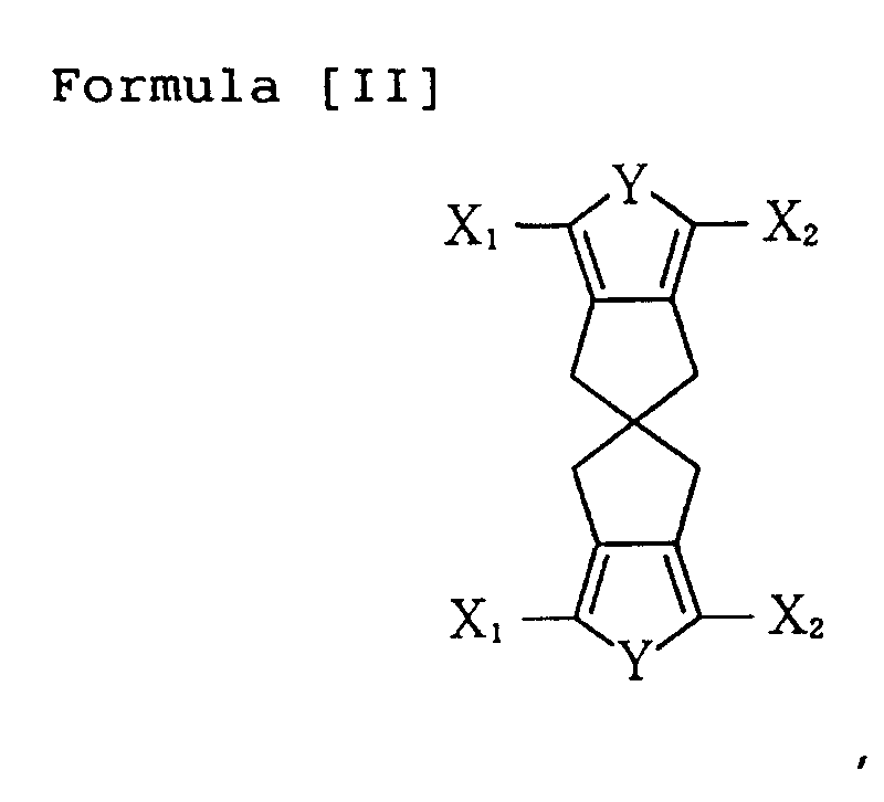
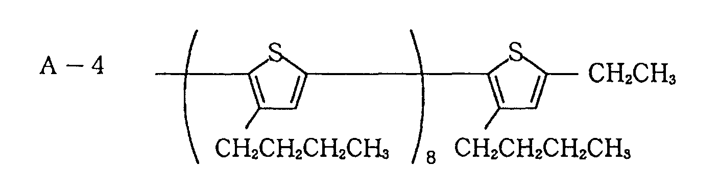
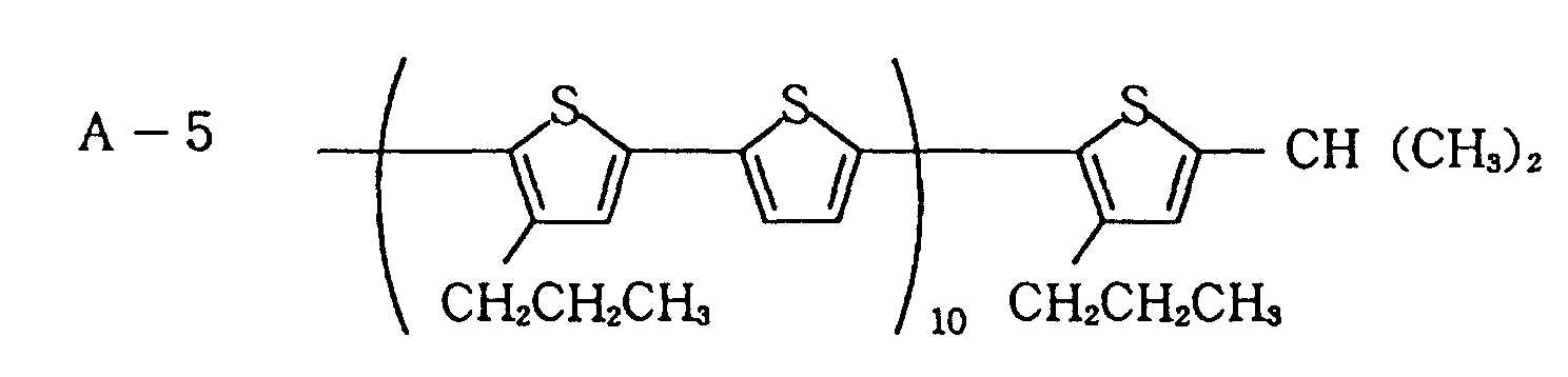
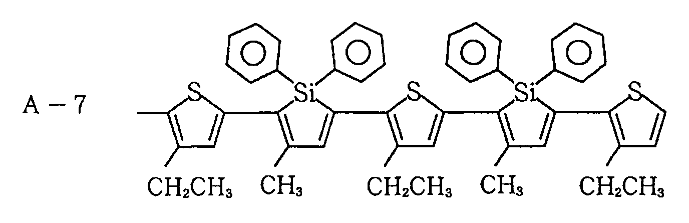
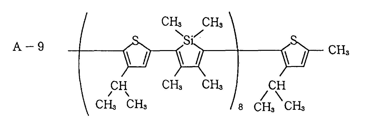
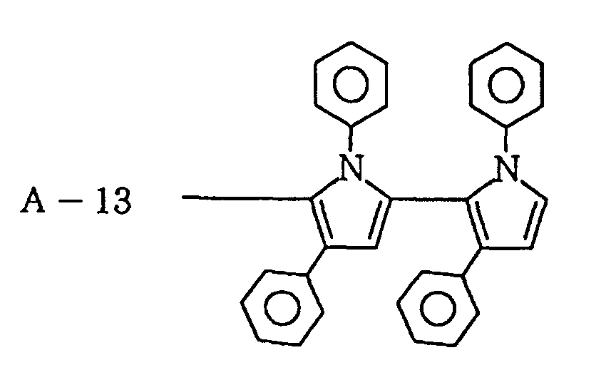
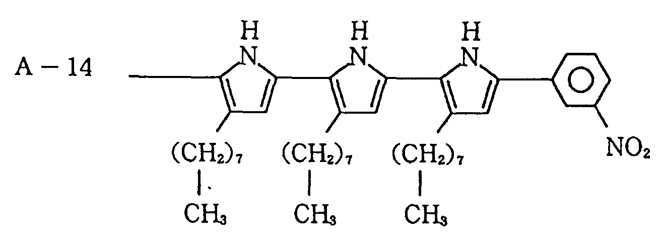
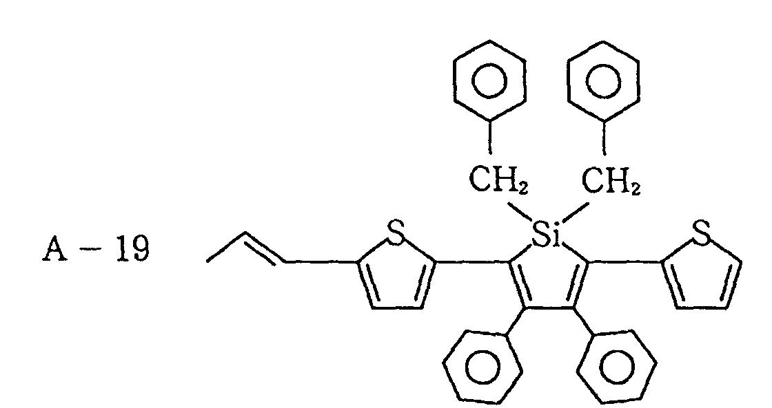
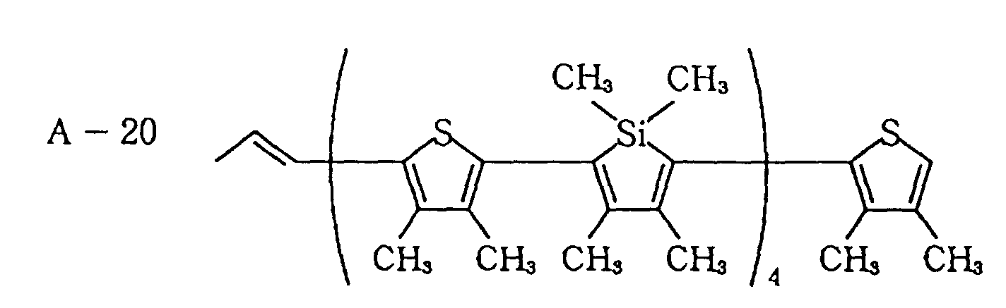
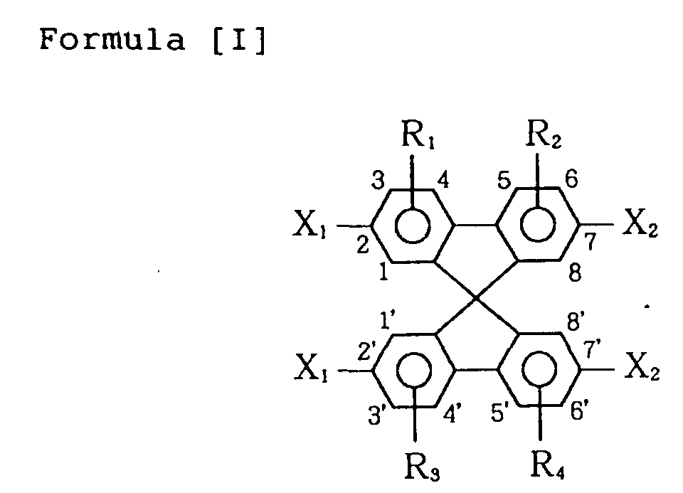
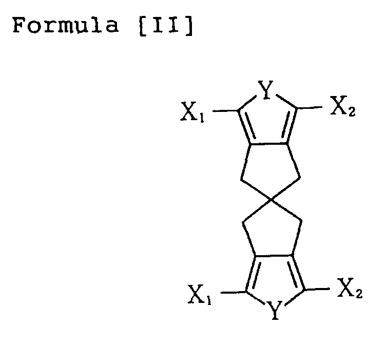
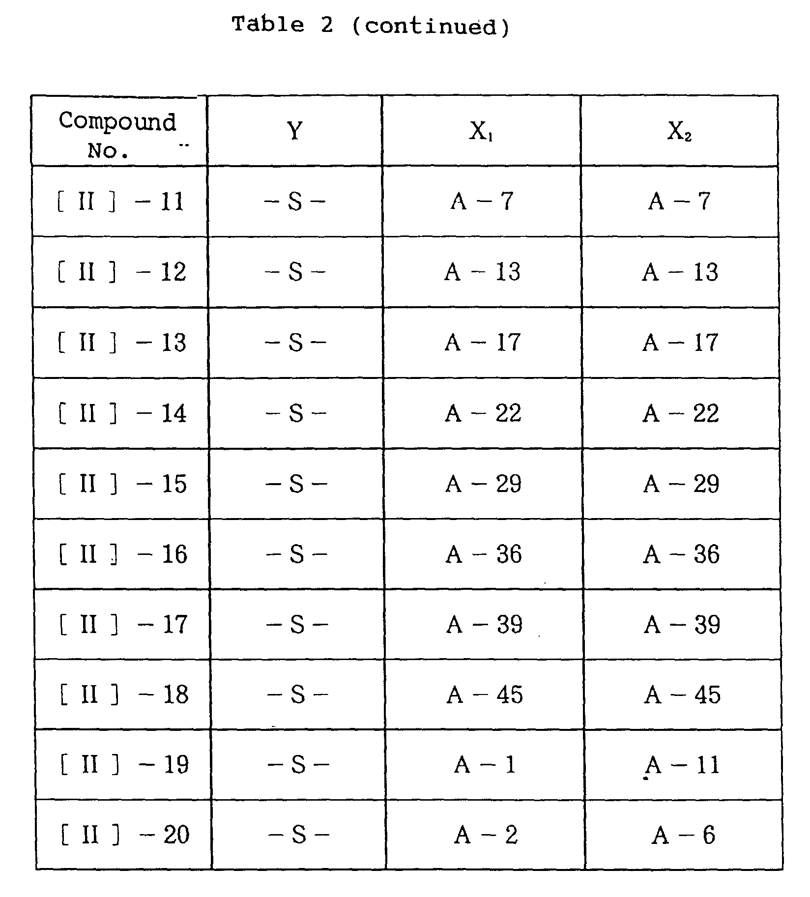
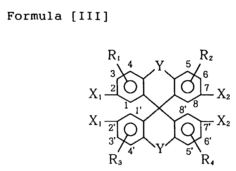
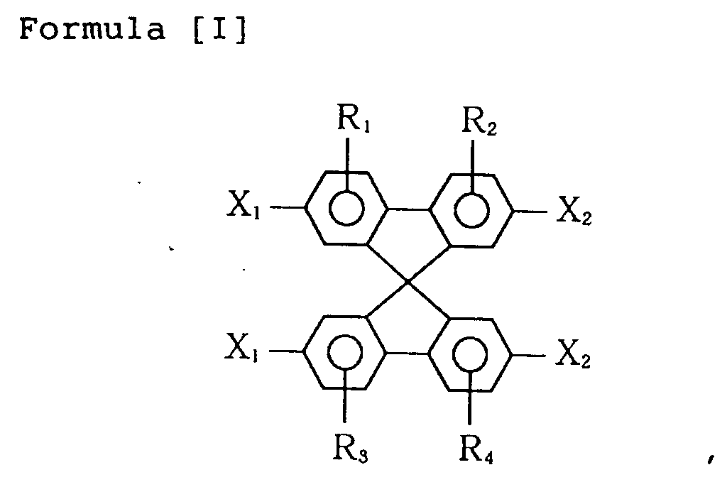
- an organic luminescence device comprising: a pair of electrodes comprising an anode and a cathode, and a layer of organic compound disposed between the electrodes; wherein the organic compound layer contains at least one species of spiro compounds represented by formulae [I], [II] and [III] shown below: and wherein R 1 , R 2 , R 3 and R 4 independently denote a hydrogen atom, an alkyl group, a substituted or unsubstituted aralkyl group, a substituted or unsubstituted aryl group, a substituted or unsubstituted heterocyclic group or a nitro group;
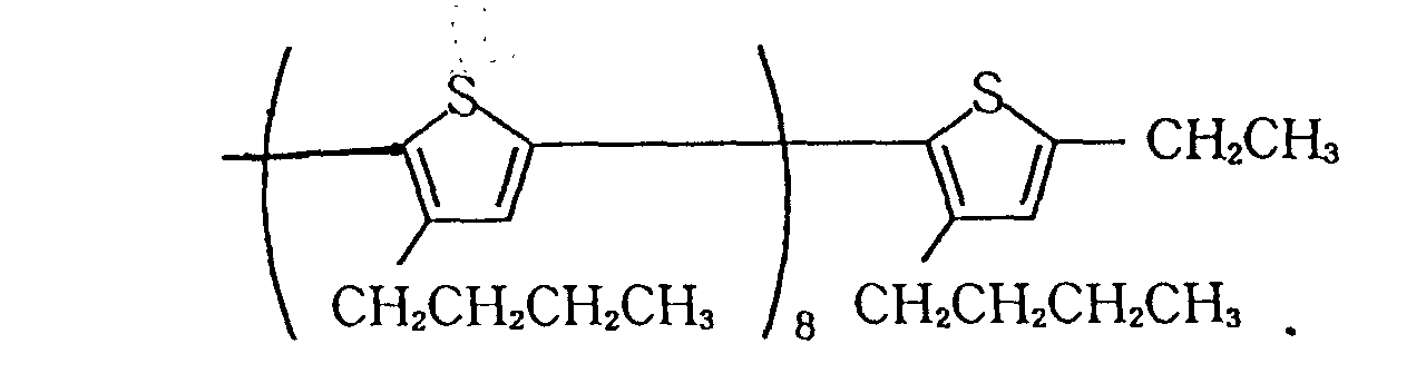
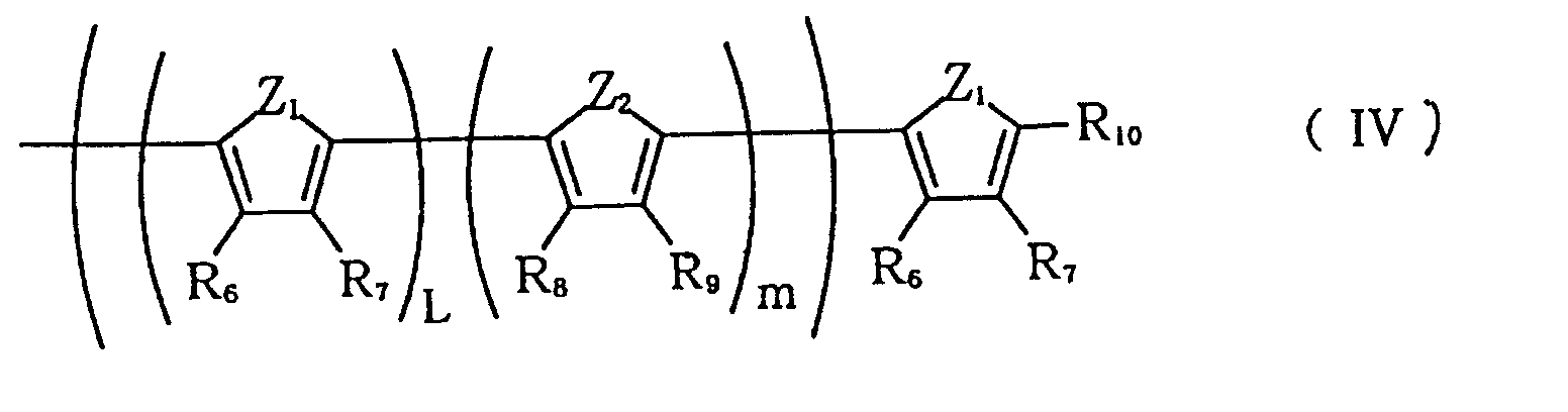
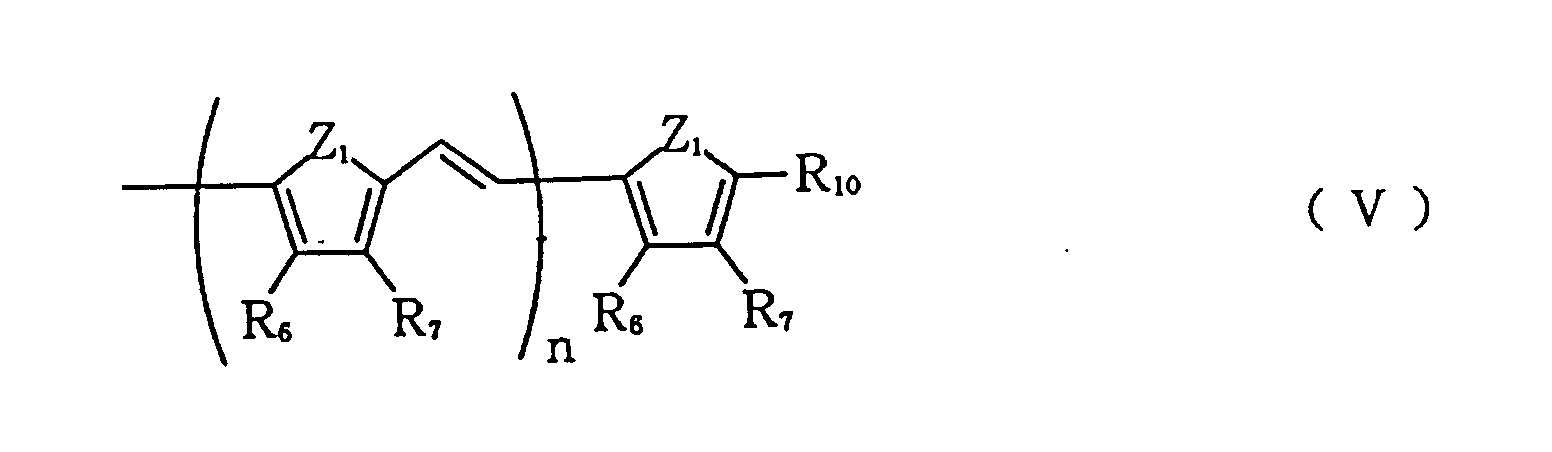
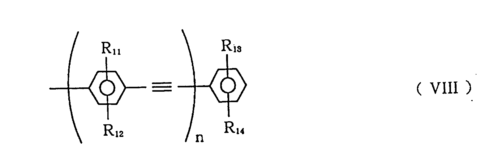
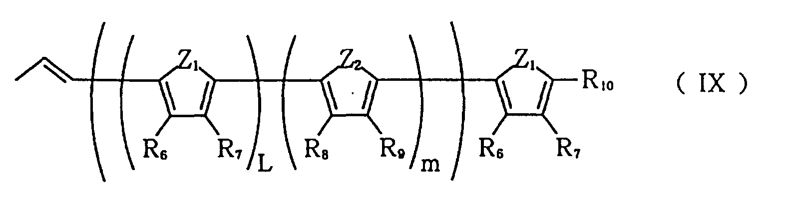
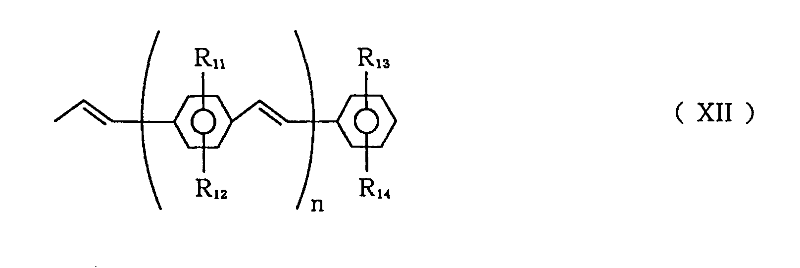
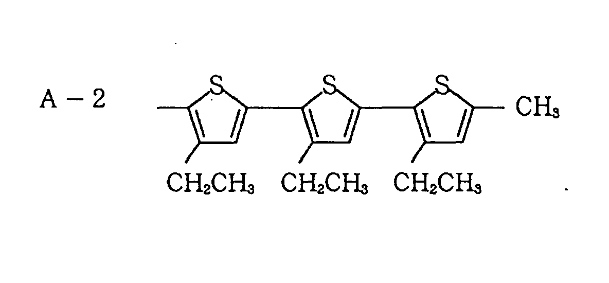
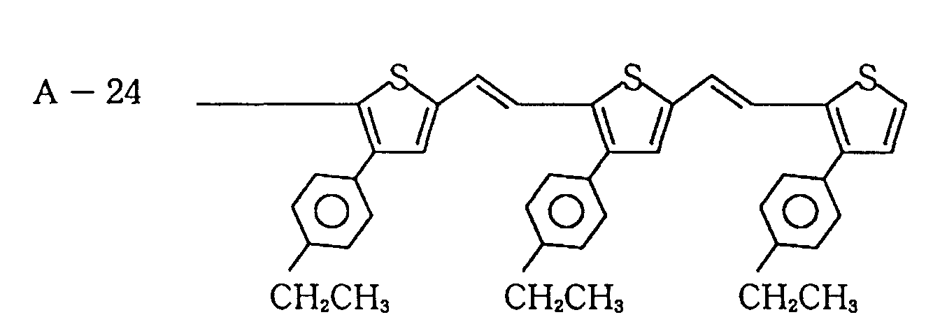
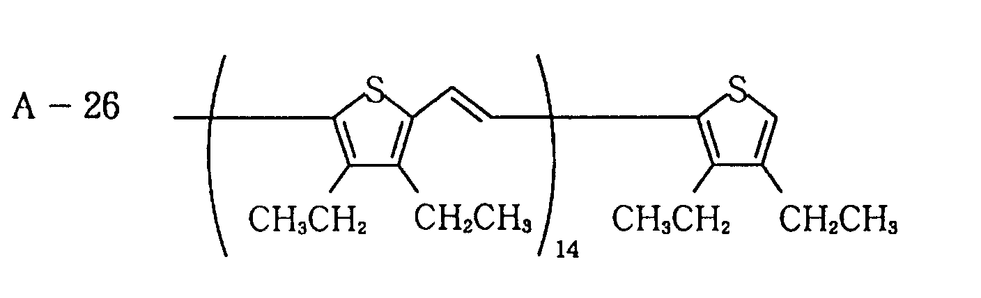
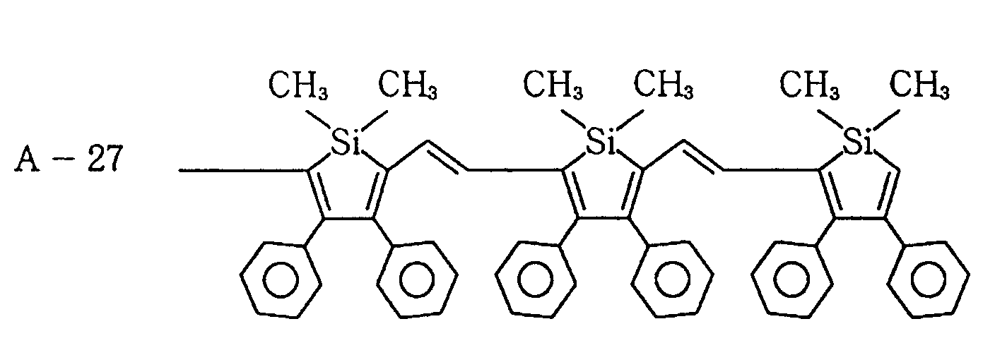
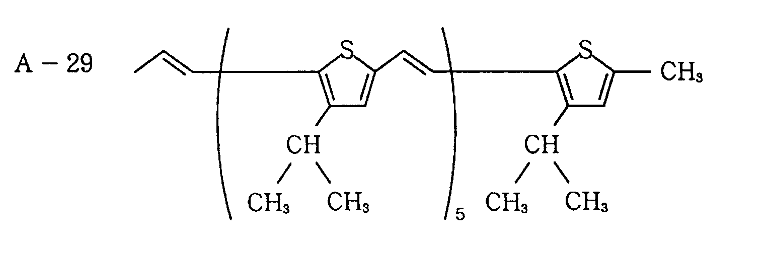
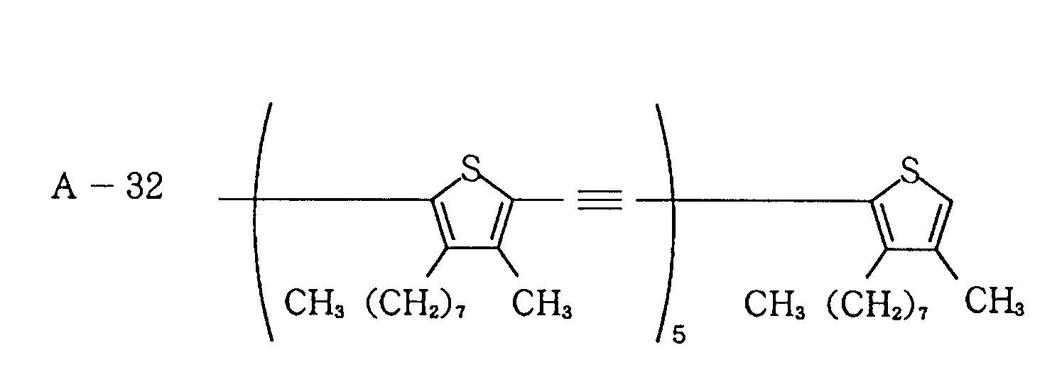
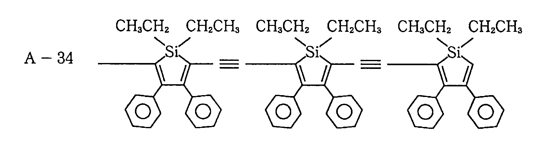
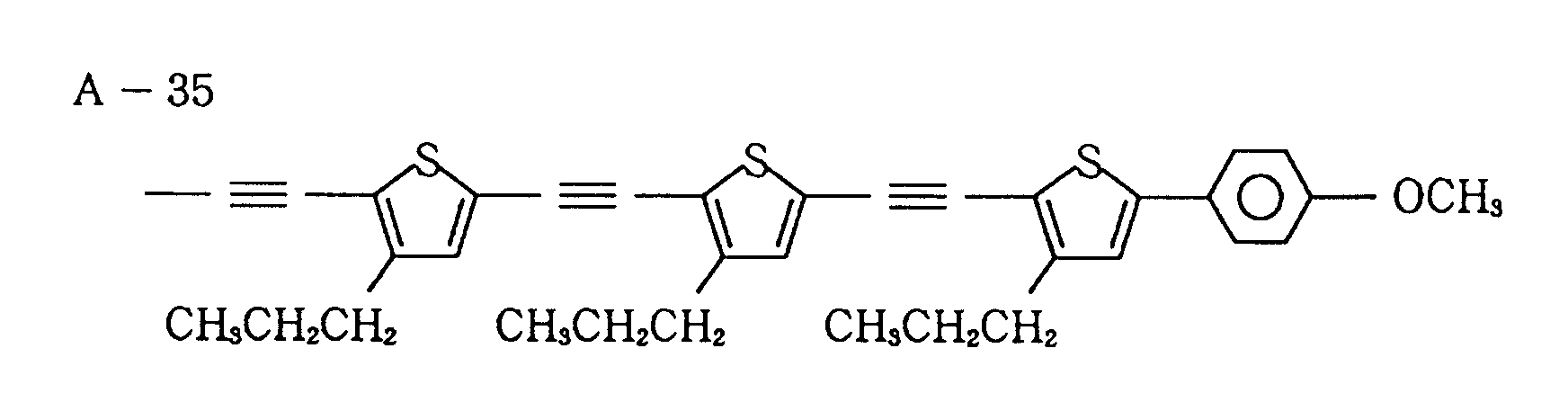
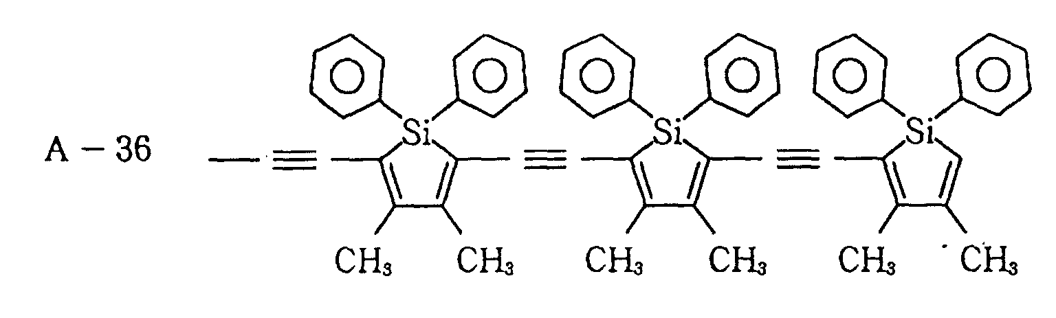
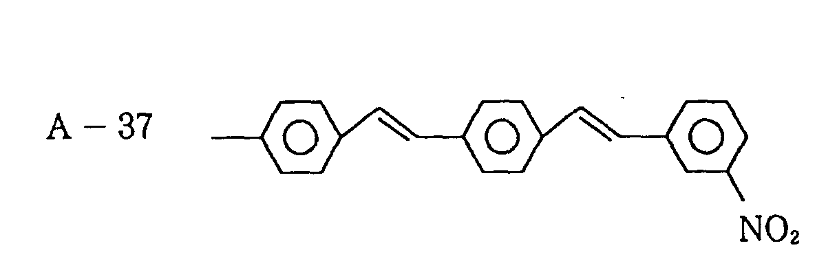
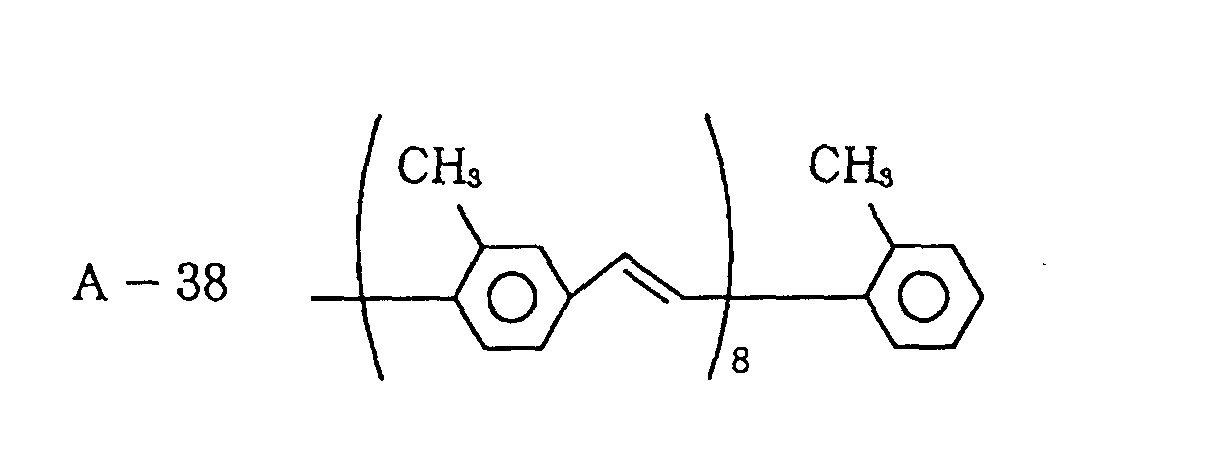
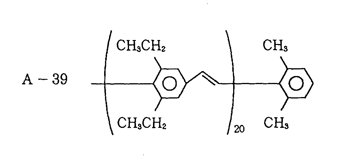
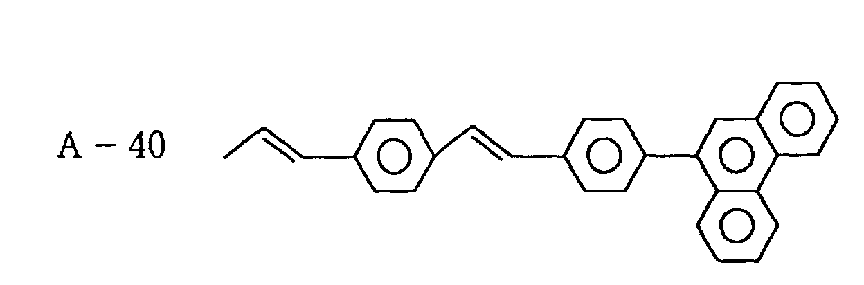
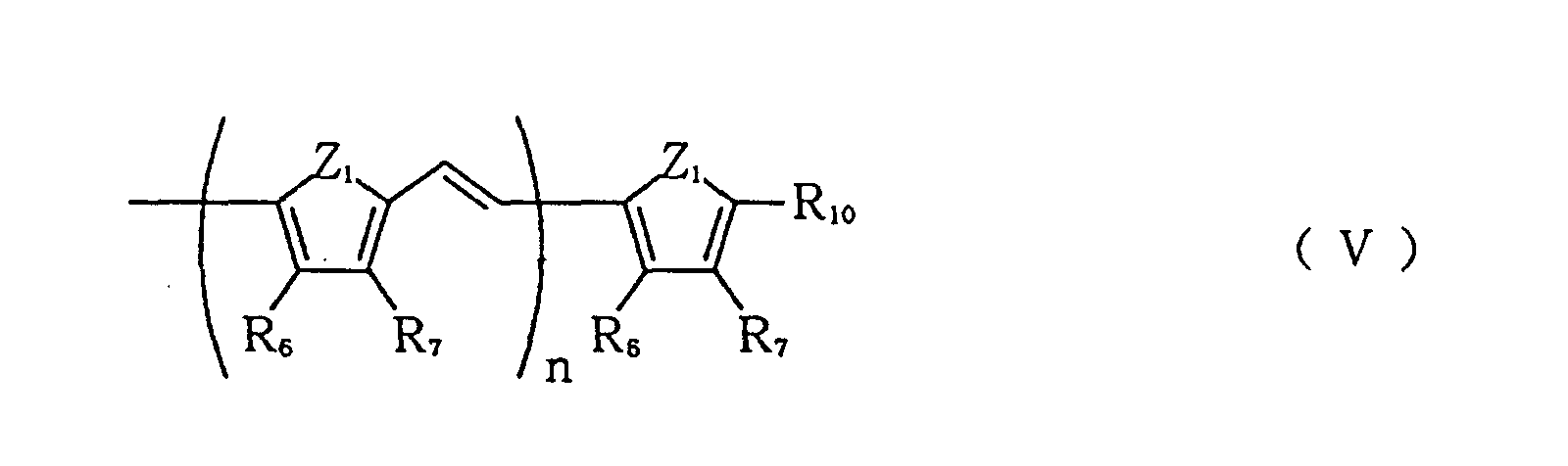
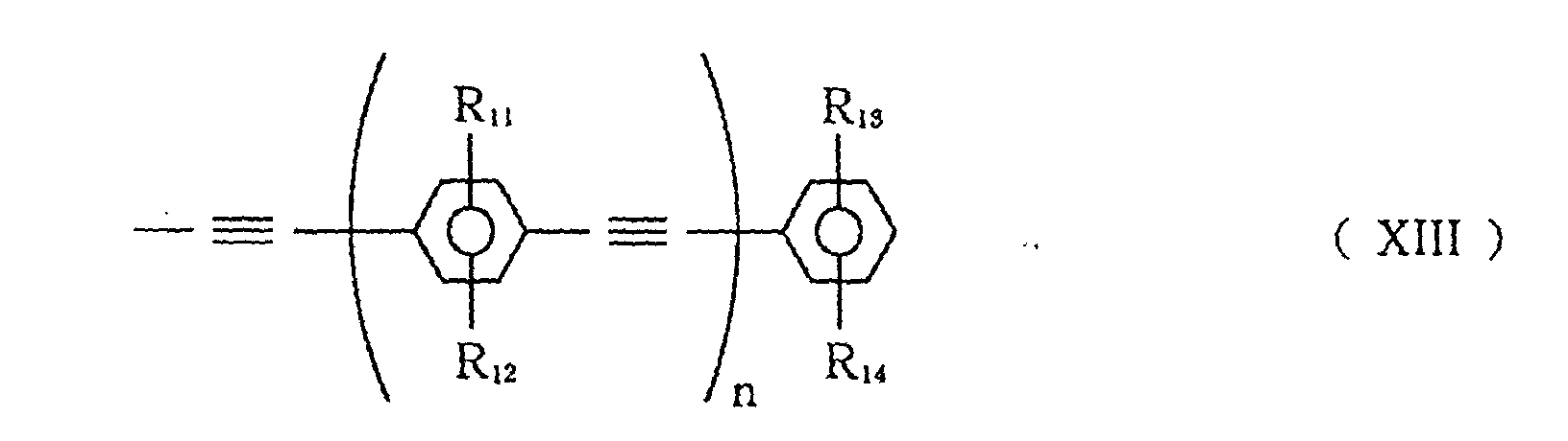
- X 1 and X 2 independently denote a hydrogen atom, an alkyl group, a substituted or unsubstituted aralkyl group, a substituted or unsubstituted aryl group, a substituted or unsubstituted heterocyclic group, a nitro group, a substituted or unsubstituted amino group, or a group selected from those represented by structural formulae (IV) - (XIII) shown below with the proviso that at least one of X 1 and X 2 is selected from groups represented by the formulae (IV) - (XIII): wherein R 6 to R 14 independently denote a hydrogen atom, an alkyl group, a substituted or unsubstituted aralkyl group, a substituted or unsubstituted aryl group, a substituted or unsubstituted heterocyclic group, an alkoxyl group, or a nitro group;
- Z 1 and Z 2 independently denote -S-, NR 15 or Si(R 16 )R 17 wherein R 15 denotes a hydrogen atom, an alkyl group, a substituted or unsubstituted aralkyl group, a substituted or unsubstituted aryl group or a substituted or unsubstituted heterocyclic group; R 16 and R 17 independently denote an alkyl group, a substituted or unsubstituted aralkyl group, a substituted or unsubstituted aryl group or a substituted or unsubstituted heterocyclic group; and
- L denotes an integer of 0 - 20
- m denotes an integer of 0 - 20 with the proviso that L+m makes an integer of 1 - 20
- n is an integer of 1 - 20.
- the organic compound layer comprising the spiro compound of the formula [I], [II] or [III] used in the present invention is useful as an electron-transporting layer, and also as a luminscence layer.
- the organic compound layer can be prepared through vacuum deposition, casting, wet-coating, etc., thus readily realizing a larger size thereof relatively inexpensively.
- Figures 1 to 3 are schematic sectional views each illustrating a basic structure of an organic luminescence device according to an embodiment of the present invention.
- the organic luminescence device is characterized in that the organic compound layer disposed between the pair of electrodes (anode and cathode) contains at least one species of spiro compound represented by the above-mentioned formulae [I] to [III].
- alkyl group is C 1 -C 8 alkyl groups and include: methyl, ethyl, n-propyl, isopropyl, n-butyl, tert-butyl, and octyl.
- aralkyl group may include: benzyl and phenethyl.
- aryl group may include: phenyl, biphenyl, terphenyl, naphthyl, anthryl and phenanthryl.
- heterocyclic group may include: thienyl, pyrrolyl, imidazolyl, furyl, pyridyl, indolyl, quinolinyl, isoquinolyl and carbazolyl.
- substituted amino group may include: methylamino, dimethylamino, ethylamino, diethylamino, benzylamino, dibenzylamino, phenylamino and diphenylamino.
- alkoxyl group is C 1 -C 8 alkoxyl groups and may include: methoxyl, ethoxyl, propoxyl; and phenoxyl.
- substituents which may be possessed by the above-mentioned substituents include: C 1 -C 8 alkyl groups, such as methyl, ethyl and propyl; aralkyl groups, such as benzyl and phenethyl; aryl groups, such as phenyl, biphenyl, terphenyl, naphthyl, anthryl and phenanthryl; heterocyclic groups, such as thienyl, pyrrolyl, imidazolyl, furyl, pyridyl, indolyl, quinolinyl, isoquinolyl and carbazolyl; and amino groups, such as amino, methylamino, dimethylamino, ethylamino, diethylamino, benzylamino, dibenzylamino, phenylamino and diphenylamino.
- C 1 -C 8 alkyl groups such as methyl, ethyl and propyl
- L+m and n in the structural formulae (IV) - (XIII) are integers of 2 - 8.
- the spiro compound of the formula [I], [II] or [III] is contained in a single luminescence layer constituting the organic compound layer, or more preferably in a luminescence layer and/or an electron-transporting layer constituting the organic compound layer of a laminated structure for achieving better luminescence performances in a longer wavelength region.
- the spiro compounds used in the present invention inclusive of those enumerated below are synthesized by, e.g., a method as reported by James M, Tour; Journal of Organic Chemistry, Vol. 61 , pp. 6906- (1996).
- the organic compound layer comprising the above-mentioned spiro compound of the formula [I], [II.] or [III] may be formed between a pair of electrodes (anode and cathode) by vacuum deposition or wet-coating process.
- the organic compound layer may preferably be formed in a thickness of at most 10 ⁇ m, more preferably at most 0.5 ⁇ m, further preferably 0.01 - 0.5 ⁇ m.
- the organic compound layer constituting the organic luminescence device of the present invention may have a single-layer structure as shown in Figure 1 or a laminate structure of two or more layers as shown in Figures 2 and 3.
- Figure 1 is a schematic sectional view illustrating an embodiment of the organic luminescence device of the present invention.
- the organic luminescence device includes a substrate 1, and an anode 2, a luminescence layer 3 and a cathode disposed in this order on the substrate 1 so as to form a laminate structure.
- the luminescence layer 3 may comprise a single species of luminescent material exhibiting a hole-transporting function, an electron-transporting function and a luminescence function in combination or a mixture of plural compounds exhibiting these functions, respectively.
- the luminescence layer 3 may have a thickness of 5 nm to 1 ⁇ m, preferably 10 - 500 nm.
- Figure 2 is a sectional view showing a laminate structure of another embodiment of the organic luminescence device.
- the organic luminescence device includes a substrate 1, and an anode 2, a hole-transporting layer 5, an electron-transporting layer 6 and a cathode 4 disposed successively in this order on the substrate 1 so as to form a laminate structure, either one or both of the hole-transporting layer 5 and the electron-transporting layer 6 may contain a luminescent material also having a hole-transporting function and/or an electron-transporting function, respectively, for constituting a luminescence layer 3 in combination.
- One of the layers 6 and 5 may contain a material having no luminescent function but having a good electron-transporting or hole-transporting function.
- Each of the hole-transporting layer 5 and the electron-transporting layer 6 may have a thickness of 5 nm to 1 ⁇ m, preferably 10 - 500 nm.
- FIG. 3 is a sectional view showing still another embodiment of the organic luminescence device of the present invention.
- the organic luminescence device includes a substrate 1, and an anode 2, a hole-transporting layer 5, a luminescence layer 3, an electron-transporting layer 6 and a cathode 4 disposed successively in this order on the substrate 1 to form a laminate structure.
- the carrier transporting functions and the luminescent function of the organic compound layer are separated and assigned to the respective layers.
- Each of the hole-transporting layer 5, the luminescence layer 3 and the electron-transporting layer 6 may contain a single species or plural species of compounds showing respectively expected functions so as to exhibit desired performances. More specifically, in the case of using plural species of compounds in combination, a lot of latitude is provided in selection of materials for each layer, and various compounds having different emission wavelengths can be used to provide a variety of luminescence hues.
- each of the hole-transporting layer 5, the luminescence layer 3 and the electron-transporting layer 6 may have a thickness of 5 nm - 1 ⁇ m, preferably 10 - 500 nm.
- Figures 1 - 3 described above merely show basic structures of the organic luminescence device according to the present invention, and various modifications thereof are possible.
- an electron injection layer on the cathode side
- a hole injection layer on the anode side
- an insulating layer on the anode side
- an adhesive layer on the adhesive layer
- an interference layer on the hole-transporting layer 5
- the hole-transporting layer 5 can be divided into two layers with different ionization potentials.
- the spiro compounds represented by the formula [I], [II] or [III] have better electron-transporting performance, luminescence performance and durability than conventional compounds and can be adopted in any of the device structures shown in Figures 1 to 3.
- the organic compound layer containing the spiro compound is particularly useful as an electron-transporting layer and/or a luminescence layer.
- a layer thereof may be formed by vacuum deposition or solution coating in a form which is not liable to crystallize and is excellent in stability with time.
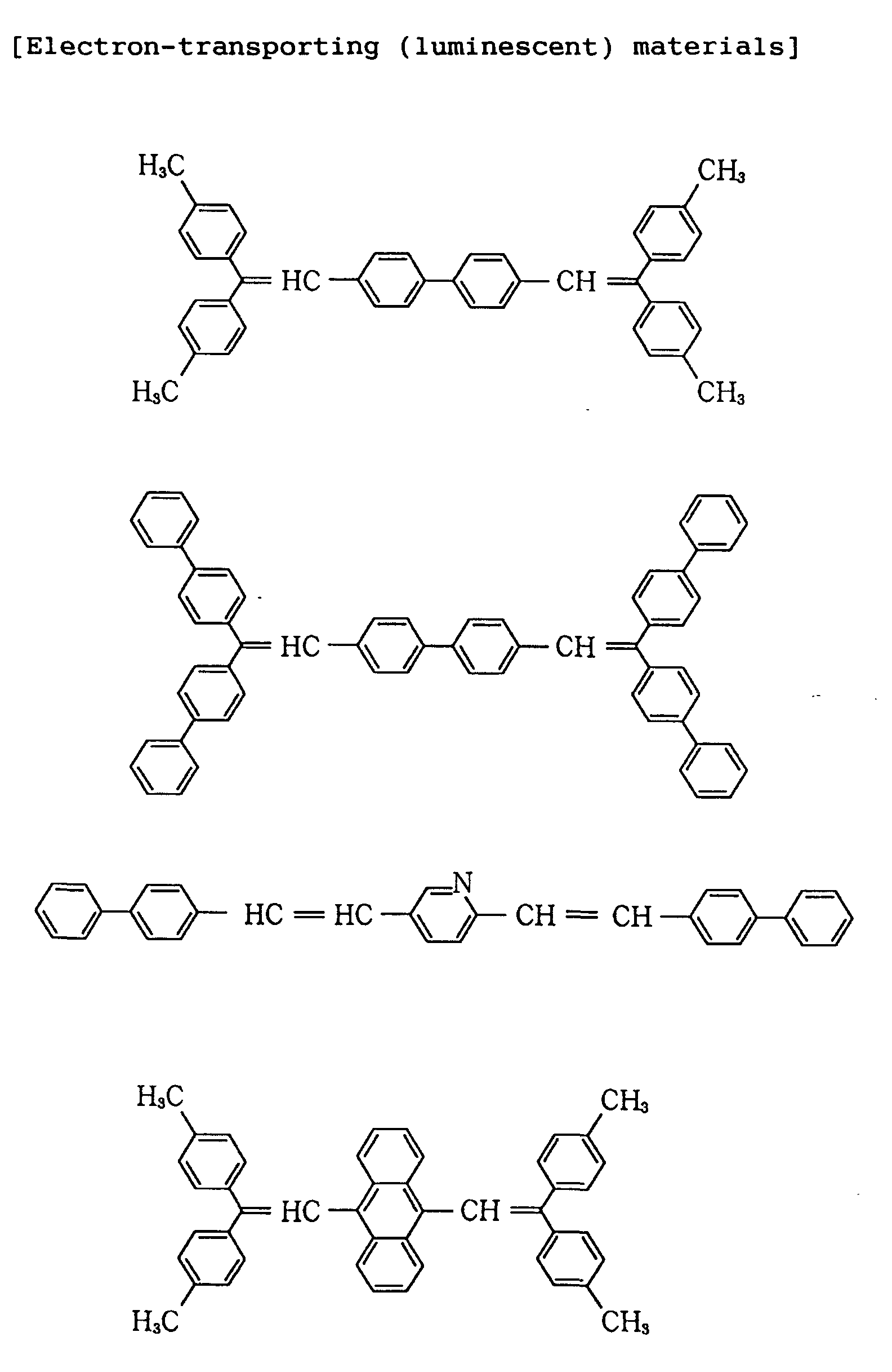
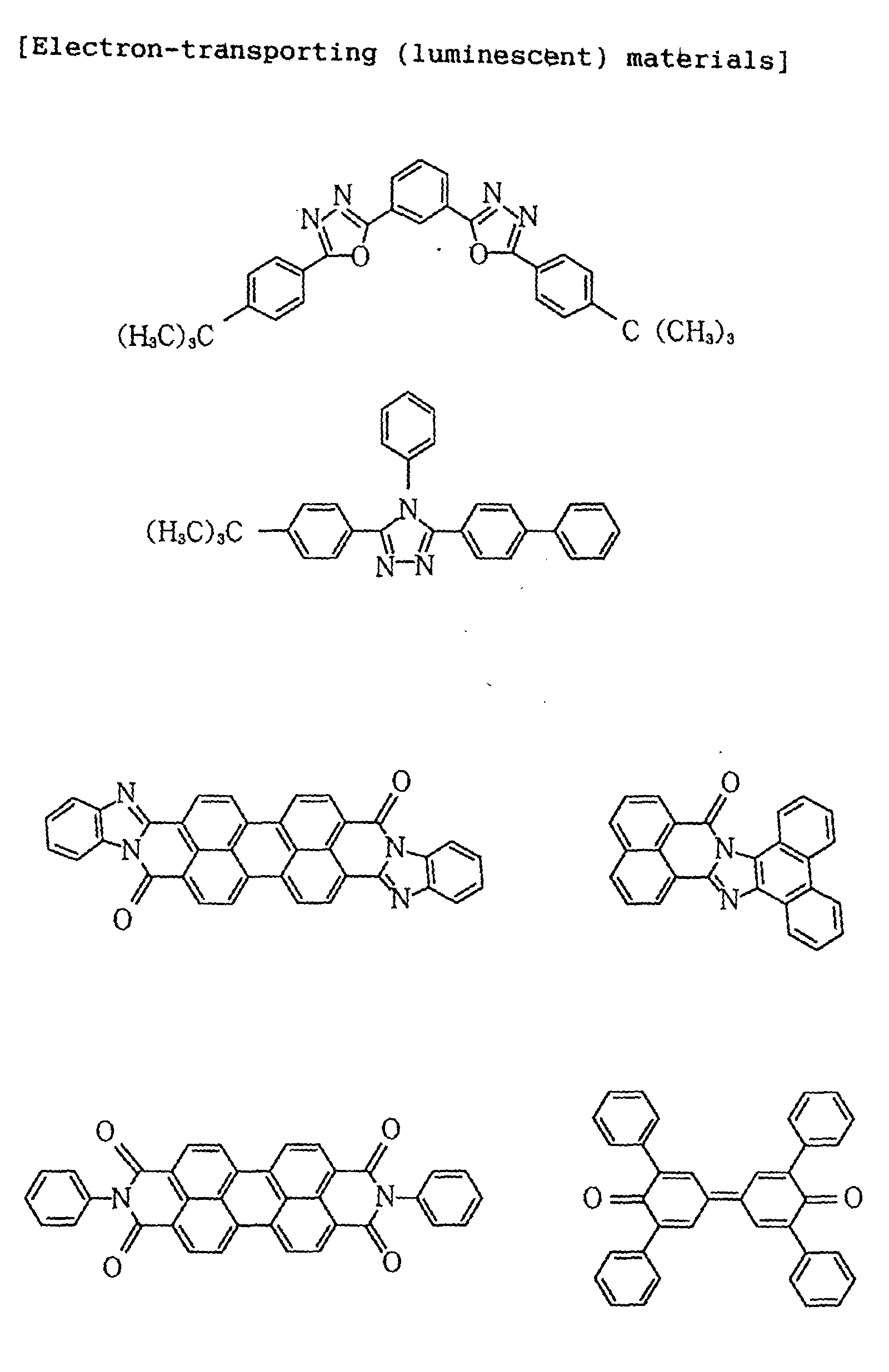
- the spiro compounds of the formula [I], [II] or [III] can be used to constitute an electron-transporting layer and/or a luminescence layer, as desired, in combination with a known hole-transporting compound, luminescent compound or electron-transporting compound, examples of which are enumerated hereinbelow.
- the organic compound layer containing the spiro compound of the formula [I], [II] or [III] or other organic compound layers may be formed into film by vacuum deposition or coating of a solution of the relevant compound in an appropriate solvent.
- the organic compound can be used in mixture with an appropriate binder resin to form a film.
- the organic compound, inclusive of the spiro compound of the formula [I], [II] or [III] may for example be used in 0.1 - 10 wt. parts per 100 wt. parts of the binder resin.
- the binder resin used for the above purpose may be selected from a wide variety of scope. Examples thereof may include: polyvinyl carbazole resin, polycarbonate resin, polyester resin, polyarylate resin, polystyrene resin, acrylic resin, methacrylic resin, butyral resin, polyvinyl acetal resin, diallyl phthalate resin, phenolic resin, epoxy resin, silicone resin, polysulfone resin, and urea resin. These resins may be used singly or in combination of two or more species or in the form of copolymers.
- the anode As a material for the anode (2 shown in Figures 1 - 3), it is preferred to use one having as large a work function as possible, examples of which may include: metals, such as gold, platinum, nickel, palladium, cobalt, selenium and vanadium, and their alloys; metal oxides, such as tin oxide, zinc oxide, indium tin oxide (ITO), and indium zinc oxide; and electroconductive polymers, such as polyaniline, polypyrrole, polythiophene, and polyphenylene sulfide. These compounds may be used singly or in combination of two or more species.
- metals such as gold, platinum, nickel, palladium, cobalt, selenium and vanadium, and their alloys
- metal oxides such as tin oxide, zinc oxide, indium tin oxide (ITO), and indium zinc oxide
- electroconductive polymers such as polyaniline, polypyrrole, polythiophene, and polyphenylene sulfide.
- the cathode 4 shown in Figures 1 - 3 it is preferred to use one having a small work function, examples of which may include: metals, such as lithium, sodium, potassium, calcium, magnesium, aluminum, indium, silver, lead, tin and chromium, and their alloys. It is also possible to use metal oxide, such as indium tin oxide (ITO).
- ITO indium tin oxide
- the cathode may be formed in a single layer or a lamination of plural layers.
- the substrate 1 shown in Figures 1 - 3 for the organic luminescence device of the present invention may include an opaque substrate of metal, ceramics, etc., and a transparent substrate of glass, quartz, plastics, etc. It is possible to form the substrate with a color filter film, a fluorescent color conversion film, a dielectric reflection film, etc., thus controlling emitted luminescent light.
- the organic luminescence device of the present invention may further include a protective layer or a sealing layer.
- the protective layer may include: an inorganic film of diamond, metal oxide, metal nitride, etc.; a polymer film of fluorine-containing resin, polyparaxylene, polyethylene, silicone resin, polystyrene, etc., and a film of light-curable resin. It is also possible to effect packaging of the organic luminescence device per se with a sealing resin while covering the organic luminescence device with glass, gas-impermeable film, metal, etc.
- An electroluminescence device of a structure as shown in Figure 2 was prepared in the following manner.
- a 1.1 mm-thick glass substrate coated with a 120 nm-thick film of ITO (indium tin oxide) formed by sputtering was successively washed with acetone and isopropyl alcohol (IPA) under application of ultrasonic wave and then washed with IPA under boiling, followed by cleaning by UV/ozone (i.e., irradiation with ultraviolet rays in an ozone-containing atmosphere), to obtain a transparent conductive substrate (including a substrate 1 and an ITO anode 2 formed thereon).
- ITO indium tin oxide
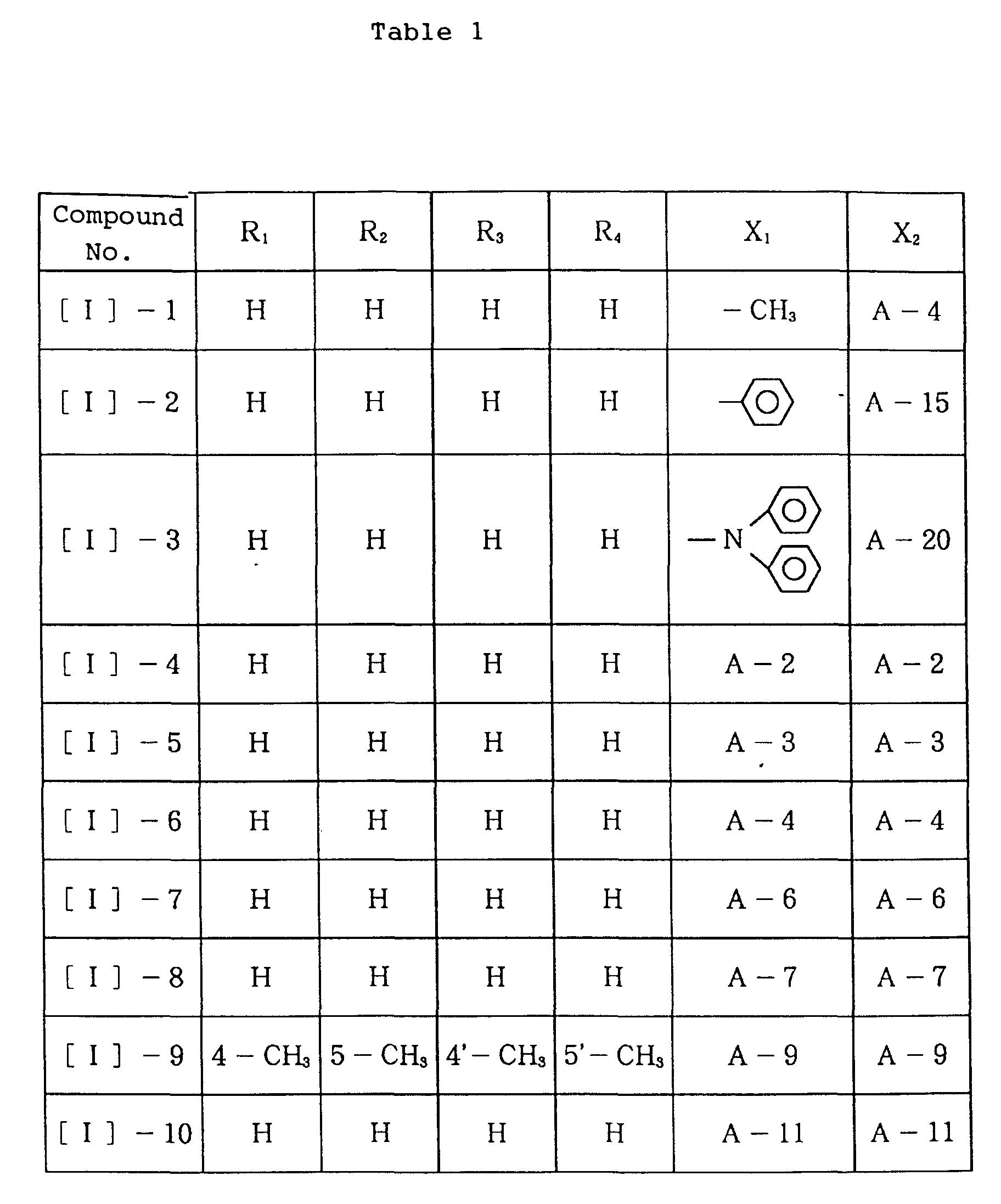
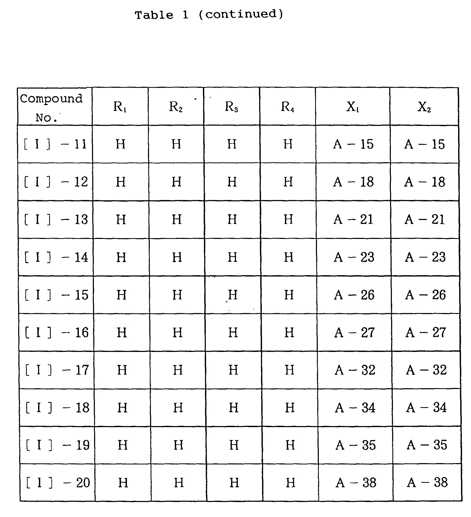
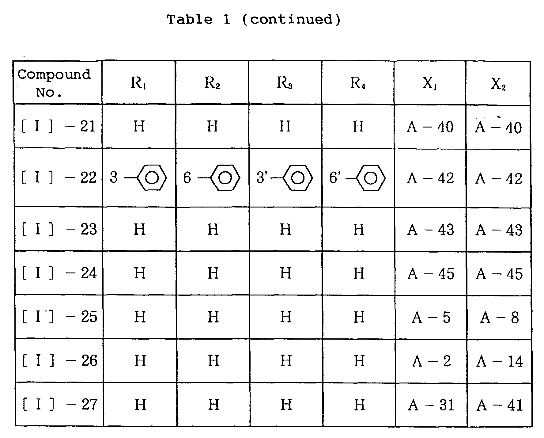
- the transparent conductive substrate was coated by vacuum deposition of a compound (TPD) represented by a structural formula shown below: to form a 60 nm-thick hole-transporting layer 5 and then by vacuum deposition of a spiro compound (Compound No. I-4 listed in Table 1) to form a 60 nm-thick electron-transporting layer 6.
- TPD a compound represented by a structural formula shown below: to form a 60 nm-thick hole-transporting layer 5 and then by vacuum deposition of a spiro compound (Compound No. I-4 listed in Table 1) to form a 60 nm-thick electron-transporting layer 6.
- the vacuum deposition was respectively performed in a vacuum of 1.0x10 -4 Pa and at a film thickness growth rate of 0.2 - 0.3 nm/sec.
- the electron-transporting layer was further coated by vacuum deposition of Al-Li alloy (Li content: 1 atom %) to form a 150 nm-thick metal film 4 under a vacuum of 1.0x10 -4 Pa and at a film thickness growth rate of 1.0 - 1.2 nm/sec, thereby forming an organic luminescence device of a structure shown in Figure 2.
- Al-Li alloy Li content: 1 atom %
- the thus-obtained device was then supplied with a DC voltage of 8 volts between the ITO electrode 2 as an anode and the Al-Li alloy electrode as a cathode, whereby a current flowed at a density of 8.2 mA/cm 2 and red luminescence was observed at a luminance of 550 cd/m 2 .
- the device was further subjected to 100 hours of continuous voltage application at a constant current density of 7.0 mA/cm 2 in a nitrogen atmosphere, whereby the device initially exhibited a luminance of 505 cd/m 2 , which was lowered to 460 cd/m 2 after 100 hours, thus showing only a small luminance deterioration.
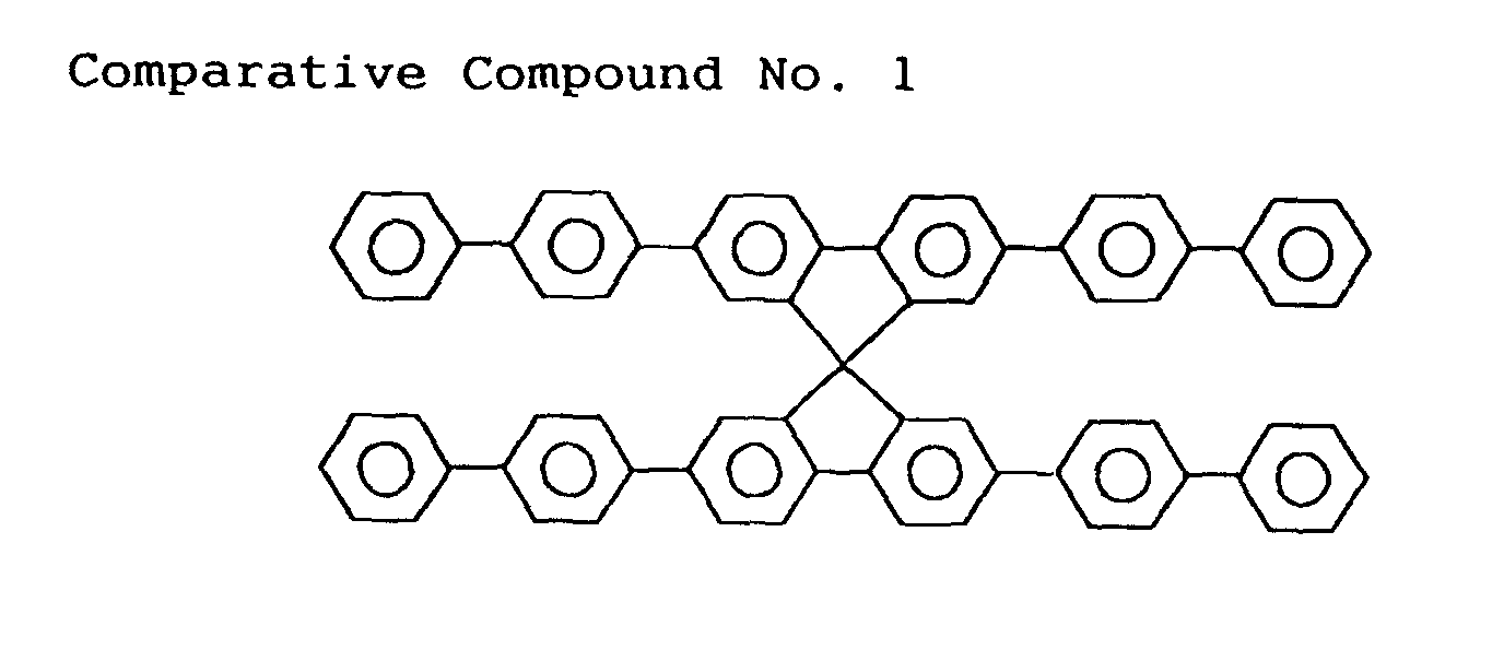
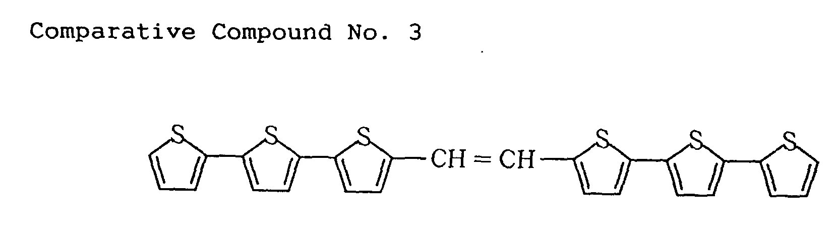
- Comparative organic luminescence devices were prepared and evaluated in the same manner as in Example 1 except for using Comparative Compound Nos. 1 - 3, respectively, shown below, instead of Compound No. I-4. The results are also shown in Table 4.
- Example 1 The procedure of Example 1 was repeated up to the formation of the hole-transporting layer 5.
- the hole-transporting layer 5 was further coated by vacuum deposition of a mixture of spiro compound (Compound No. I-1) and aluminum tris(quinolinol) in a weight ratio of 1:20 to form a 60 nm-thick electron-transporting layer 6 under a vacuum of 1.0x10 -4 Pa and at a film thickness growth rate of 0.2 - 0.3 nm/sec.
- a mixture of spiro compound Compound No. I-1
- aluminum tris(quinolinol) in a weight ratio of 1:20 to form a 60 nm-thick electron-transporting layer 6 under a vacuum of 1.0x10 -4 Pa and at a film thickness growth rate of 0.2 - 0.3 nm/sec.
- the electron-transporting layer was further coated by vacuum deposition of Al-Li alloy (Li content: 1 atom. %) to form a 150 nm-thick metal film 4 under a vacuum of 1.0x10 -4 Pa and at a film thickness growth rate of 1.0 - 1.2 nm/sec, thereby forming an organic luminescence device of a structure shown in Figure 2.
- Al-Li alloy Li content: 1 atom. %
- the thus-obtained device was then supplied with a DC voltage of 8 volts between the ITO electrode 2 as an anode and the Al-Li alloy electrode as a cathode, whereby a current flowed at a density of 8.7 mA/cm 2 and red luminescence was observed at a luminance of 540 cd/m 2 .
- the device was further subjected to 100 hours of continuous voltage application at a constant current density of 7.0 mA/cm 2 in a nitrogen atmosphere, whereby the device initially exhibited a luminance of 500 cd/m 2 , which was lowered to 360 cd/m 2 after 100 hours, thus showing only a small luminance deterioration.
- Comparative organic compound devices were prepared and evaluated in the same manner as in Example 21 except for using Comparative Compound Nos. 1 - 3, respectively, shown above, instead of Compound No. I-1. The results are also shown in Table 5.
- Initial Luminance at 7.0mA/cm 2
- Initial (cd/m 2 ) After 100 hrs.
- Example 1 The procedure of Example 1 was repeated up to the formation of the hole-transporting layer 5.
- the hole-transporting layer 5 was further coated by vacuum deposition of aluminum tris(quinolinol) to form a 25 nm-thick luminescence layer 3 and then by vacuum deposition of a spiro compound (Compound No. I-5) to form a 40 nm-thick electron-transporting layer 6, respectively under a vacuum of 1.0x10 -4 Pa and at a film thickness growth rate of 0.2 - 0.3 nm/sec.
- a spiro compound Compound No. I-5
- the electron-transporting layer was further coated by vacuum deposition of Al-Li alloy (Li content: 1 atom. %) to form a 150 nm-thick metal film 4 under a vacuum of 1.0x10 -4 Pa and at a film thickness growth rate of 1.0 - 1.2 nm/sec, thereby forming an organic luminescence device of a structure shown in Figure 3.
- Al-Li alloy Li content: 1 atom. %
- the thus-obtained device was then supplied with a DC voltage of 10 volts between the ITO electrode 2 as an anode and the Al-Li alloy electrode as a cathode, whereby a current flowed at a density of 12.3 mA/cm 2 and orange luminescence was observed at a luminance of 1470 cd/m 2 .
- the device was further subjected to 100 hours of continuous voltage application at a constant current density of 10.0 mA/cm 2 in a nitrogen atmosphere, whereby the device initially exhibited a luminance of 1280 cd/m 2 , which was lowered to 1200 cd/m 2 after 100 hours, thus showing only a small luminance deterioration.
- Comparative organic luminescence devices were prepared and evaluated in the same manner as in Example 33 except for using Comparative Compound Nos. 1 - 3, respectively, shown above, instead of Compound No. I-5. The results are also shown in Table 6.
- Initial Luminance at 7.0mA/cm 2
- Initial (cd/m 2 ) After 100 hrs.
- a spiro compound Compound No. I-4
- the luminescence layer was further coated by vacuum deposition of Al-Li alloy (Li content: 1 atom %) to form a 150 nm-thick metal film 4 under a vacuum of 1.0x10 -4 Pa and at a film thickness growth rate of 1.0 - 1.2 nm/sec, thereby forming an organic luminescence device of a structure shown in Figure 1.
- Al-Li alloy Li content: 1 atom %
- the thus-obtained device was then supplied with a DC voltage of 10 volts between the ITO electrode 2 as an anode and the Al-Li alloy electrode as a cathode, whereby a current flowed at a density of 9.3 mA/cm 2 and red luminescence was observed at a luminance of 350 cd/m 2 .
- An organic luminescence device was prepared in the same manner as in Example 46 except for using Comparative Compound No. 2 instead of Comparative Example No. I-4.
- the resultant device was similarly supplied with a DC voltage of 10 volts, whereby a current followed at a density of 8.1 mA/cm 2 and yellow-green luminescence was observed at a luminance of 25 cd/m 2 .
- the organic luminescence device of the invention may be used, for example, as a display device, a photoindicator or a light source, such as in printers or facsimile apparatus.
Landscapes
- Chemical & Material Sciences (AREA)
- Engineering & Computer Science (AREA)
- Materials Engineering (AREA)
- Physics & Mathematics (AREA)
- Spectroscopy & Molecular Physics (AREA)
- Organic Chemistry (AREA)
- Optics & Photonics (AREA)
- Electroluminescent Light Sources (AREA)
Abstract

Description































| Example | Compound No. | Initial | Luminance (at 7.0mA/cm2) | ||
| Voltage (V) | Luminance (cd/m2) | Initial (cd/m2) | After 100 hrs. (cd/m2) | ||
| 1 | I-4 | 8 | 550 | 505 | 460 |
| 2 | I-6 | 8 | 540 | 500 | 460 |
| 3 | I-7 | 8 | 355 | 310 | 280 |
| 4 | I-10 | 8 | 340 | 290 | 260 |
| 5 | I-13 | 8 | 200 | 170 | 145 |
| 6 | I-21 | 8 | 165 | 140 | 115 |
| 7 | I-25 | 8 | 310 | 270 | 235 |
| 8 | II-1 | 8 | 170 | 130 | 110 |
| 9 | II-5 | 8 | 200 | 165 | 135 |
| 10 | II-7 | 8 | 170 | 130 | 105 |
| 11 | II-10 | 8 | 590 | 540 | 485 |
| 12 | II-12 | 8 | 145 | 120 | 100 |
| 13 | II-15 | 8 | 350 | 310 | 275 |
| 14 | II-23 | 8 | 210 | 170 | 145 |
| 15 | II-28 | 8 | 160 | 130 | 105 |
| 16 | II-33 | 8 | 140 | 120 | 90 |
| 17 | III-4 | 8 | 330 | 280 | 245 |
| 18 | III-7 | 8 | 150 | 120 | 95 |
| 19 | III-9 | 8 | 350 | 315 | 280 |
| 20 | III-11 | 8 | 170 | 135 | 110 |
| Comp. 1 | Comp. No. 1 | 8 | 45 | 40 | 10 |
| Comp. 2 | Comp. No. 2 | 8 | 80 | 55 | 20 |
| Comp. 3 | Comp. No. 3 | 8 | 25 | 20 |
| Initial | Luminance (at 7.0mA/cm2) | ||||
| Example | Compound No. | Voltage (V) | Luminance (cd/m2) | Initial (cd/m2) | After 100 hrs. (cd/m2) |
| 21 | I-1 | 8 | 540 | 500 | 460 |
| 22 | I-8 | 8 | 760 | 715 | 660 |
| 23 | I-11 | 8 | 555 | 520 | 490 |
| 24 | I-16 | 8 | 565 | 530 | 495 |
| 25 | I-23 | 8 | 360 | 330 | 305 |
| 26 | II-2 | 8 | 745 | 700 | 670 |
| 27 | II-9 | 8 | 530 | 500 | 465 |
| 28 | II-16 | 8 | 545 | 510 | 475 |
| 29 | II-20 | 8 | 980 | 935 | 890 |
| 30 | III-2 | 8 | 1020 | 975 | 925 |
| 31 | III-6 | 8 | 530 | 500 | 455 |
| 32 | III-7 | 8 | 380 | 350 | 310 |
| Comp. 4 | Comp. No. 1 | 8 | 270 | 230 | 120 |
| Comp. 5 | Comp. No. 2 | 8 | 305 | 250 | 110 |
| Comp. 6 | Comp. No. 3 | 8 | 260 | 230 | 30 |
| Initial | Luminance (at 7.0mA/cm2) | ||||
| Example | Compound No. | Voltage (V) | Luminance (cd/m2) | Initial (cd/m2) | After 100 hrs. (cd/m2) |
| 33 | I-5 | 10 | 1470 | 1280 | 1200 |
| 34 | I-9 | 10 | 950 | 785 | 720 |
| 35 | I-12 | 10 | 1340 | 1160 | 1060 |
| 36 | I-17 | 10 | 940 | 780 | 730 |
| 37 | I-24 | 10 | 630 | 525 | 460 |
| 38 | II-3 | 10 | 930 | 765 | 710 |
| 39 | II-13 | 10 | 1280 | 1100 | 1010 |
| 40 | II-19 | 10 | 870 | 725 | 660 |
| 41 | II-25 | 10 | 960 | 820 | 730 |
| 42 | II-30 | 10 | 1450 | 1270 | 1170 |
| 43 | III-3 | 10 | 1540 | 1330 | 1220 |
| 44 | III-8 | 10 | 810 | 700 | 645 |
| 45 | III-10 | 10 | 860 | 720 | 640 |
| Comp. 7 | Comp. No. 1 | 10 | 130 | 100 | 35 |
| Comp. 8 | Comp. No. 2 | 10 | 160 | 125 | 40 |
| Comp. 9 | Comp. No. 3 | 10 | 55 | 40 |
Claims (4)
- An organic luminescence device, comprising: a pair of electrodes comprising an anode and a cathode, and a layer of organic compound disposed between the electrodes; wherein the organic compound layer contains at least one species of spiro compounds represented by formulae [I], [II] and [III] shown below:
 and
and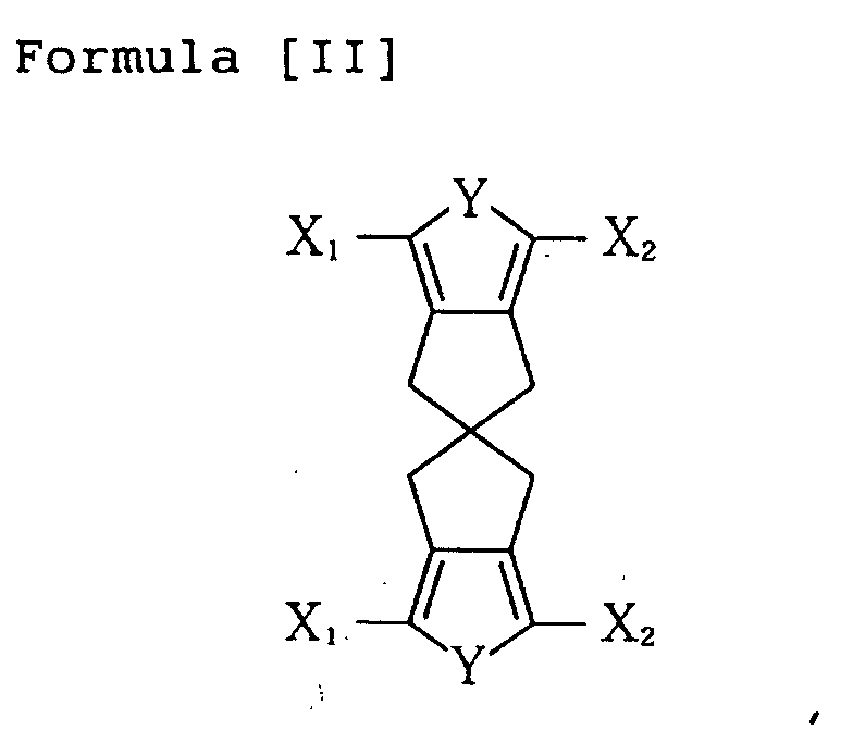 wherein
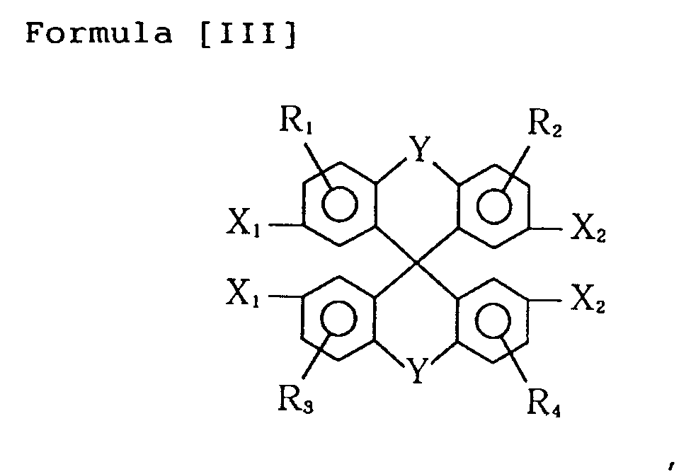 R1, R2, R3 and R4 independently denote a hydrogen atom, an alkyl group, a substituted or unsubstituted aralkyl group, a substituted or unsubstituted aryl group, a substituted or unsubstituted heterocyclic group or a nitro group;Y denotes -O-, -S-, NR5 or -CH=CH- wherein R5 denotes a hydrogen atom, an alkyl group, a substituted or unsubstituted aralkyl group, a substituted or unsubstituted aryl group, or a substituted or unsubstituted heterocyclic group; andX1 and X2 independently denote a hydrogen atom, an alkyl group, a substituted or unsubstituted aralkyl group, a substituted or unsubstituted aryl group, a substituted or unsubstituted heterocyclic group, a nitro group, a substituted or unsubstituted amino group, or a group selected from those represented by structural formulae (IV) - (XIII) shown below with the proviso that at least one of X1 and X2 is selected from groups represented by the formulae (IV) - (XIII):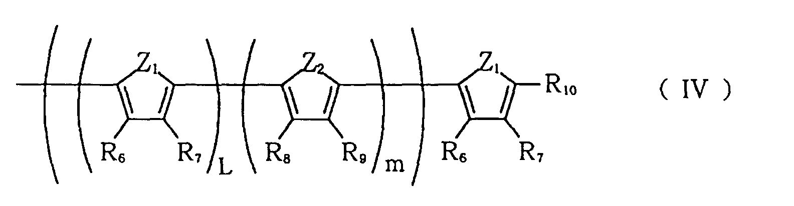

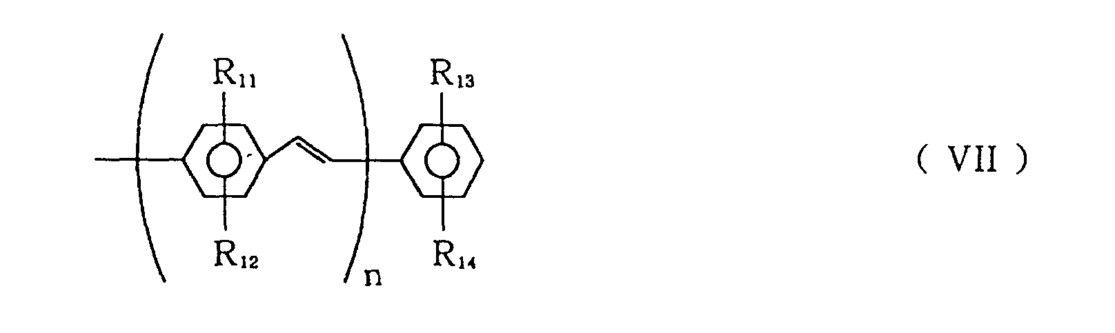


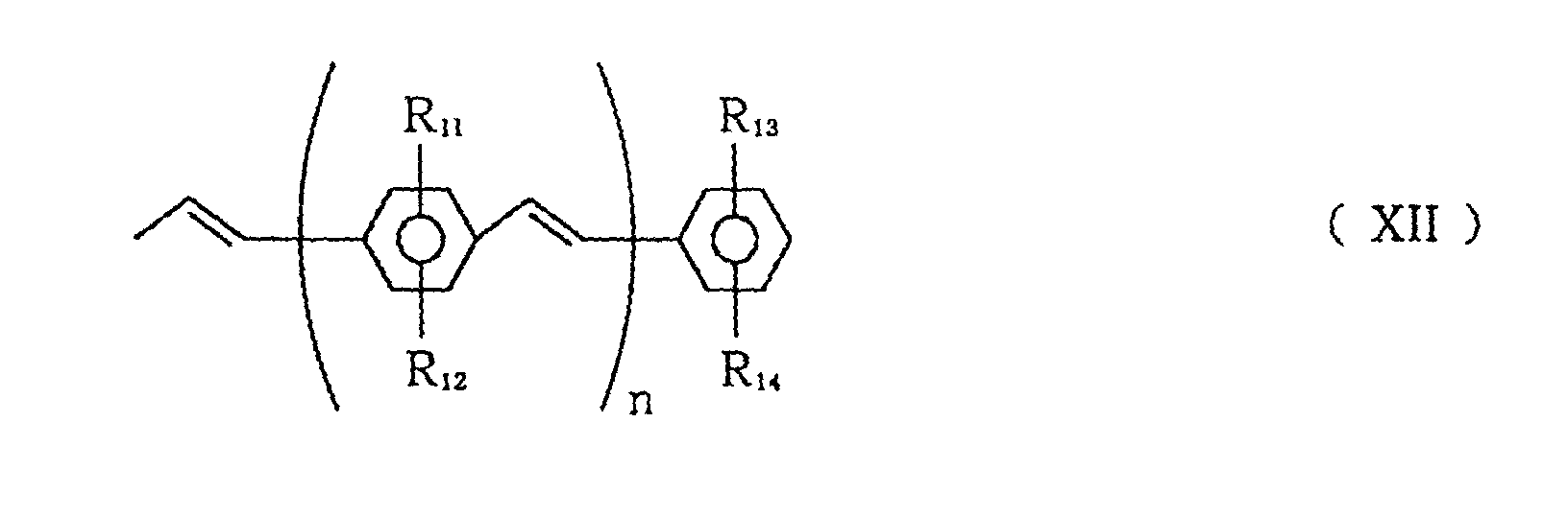 wherein R6 to R14 independently denote a hydrogen atom, an alkyl group, a substituted or unsubstituted aralkyl group, a substituted or unsubstituted aryl group, a substituted or unsubstituted heterocyclic group, an alkoxyl group, or a nitro group;
 Z1 and Z2 independently denote -S-, NR15 or Si(R16)R17 wherein R15 denotes a hydrogen atom, an alkyl group, a substituted or unsubstituted aralkyl group, a substituted or unsubstituted aryl group or a substituted or unsubstituted heterocyclic group; R16 and R17 independently denote an alkyl group, a substituted or unsubstituted aralkyl group, a substituted or unsubstituted aryl group or a substituted or unsubstituted heterocyclic group; andL denotes an integer of 0 - 20, m denotes an integer of 0 - 20 with the proviso that L+m makes an integer of 1 - 20, and n is an integer of 1 - 20.
 - An organic luminescence device according to Claim 1, wherein the organic compound layer contains a spiro compound selected from those represented by the formulae [I] to [III] wherein both X1 and X2 are groups selected from those of the formulae (IV) to (XIII).
- An organic luminescence device according to Claim 1 or claim 2 wherein the organic compound layer contains a spiro compound selected from those represented by the formulae [I] to [III] wherein both X1 and X2 are groups selected from those of the formulae (IV) to (XIII) wherein L+m and n are integers of 2 - 8.
- An organic luminescence device according to any preceding claim, wherein the organic compound layer comprises laminated layers including an electron-transporting layer and a luminescence layer, at least one of which contains at least one species of the spiro compounds represented by the formulae [I] to [III].
Applications Claiming Priority (2)
| Application Number | Priority Date | Filing Date | Title |
|---|---|---|---|
| JP2000019242 | 2000-01-27 | ||
| JP2000019242A JP3754856B2 (en) | 2000-01-27 | 2000-01-27 | Organic light emitting device |
Publications (2)
| Publication Number | Publication Date |
|---|---|
| EP1120840A2 true EP1120840A2 (en) | 2001-08-01 |
| EP1120840A3 EP1120840A3 (en) | 2005-10-26 |
Family
ID=18545975
Family Applications (1)
| Application Number | Title | Priority Date | Filing Date |
|---|---|---|---|
| EP01300728A Withdrawn EP1120840A3 (en) | 2000-01-27 | 2001-01-26 | Organic luminescence device |
Country Status (3)
| Country | Link |
|---|---|
| US (1) | US6458476B1 (en) |
| EP (1) | EP1120840A3 (en) |
| JP (1) | JP3754856B2 (en) |
Cited By (11)
| Publication number | Priority date | Publication date | Assignee | Title |
|---|---|---|---|---|
| WO2003020847A1 (en) * | 2001-09-03 | 2003-03-13 | Canon Kabushiki Kaisha | Organic luminescence device |
| FR2933238A1 (en) * | 2008-06-27 | 2010-01-01 | Commissariat Energie Atomique | NEW MESOMORPHIC ORGANIC SEMICONDUCTOR MACROMOLECULAR MATERIALS |
| US8034466B2 (en) | 2004-12-06 | 2011-10-11 | Semiconductor Energy Laboratory Co., Ltd. | Light-emitting element and light-emitting device using the same |
| CN104203955A (en) * | 2012-03-23 | 2014-12-10 | 默克专利有限公司 | 9,9,-spirodioxanthene derivatives for electroluminescent devices |
| CN107056805A (en) * | 2017-06-21 | 2017-08-18 | 中节能万润股份有限公司 | A kind of electroluminescent organic material and its application using the miscellaneous anthracene oxide of xanthene spiral shell thiophene as parent nucleus |
| CN110003024A (en) * | 2019-04-17 | 2019-07-12 | 中节能万润股份有限公司 | One kind containing the organic hole transport material and the preparation method and application thereof of spiral shell two (dibenzocycloheptene) |
| CN110343048A (en) * | 2018-04-04 | 2019-10-18 | 江苏三月光电科技有限公司 | A kind of organic compound and its application fluorene structured containing spiral shell dibenzocycloheptene |
| US10505128B2 (en) | 2014-08-01 | 2019-12-10 | Samsung Electronics Co., Ltd. | Condensed cyclic compound and organic light-emitting device including the same |
| CN110698494A (en) * | 2019-10-15 | 2020-01-17 | 浙江虹舞科技有限公司 | Charge transport material and organic light-emitting element |
| US10566547B2 (en) | 2016-07-11 | 2020-02-18 | Universal Display Corporation | Organic electroluminescent materials and devices |
| US12588409B2 (en) | 2021-01-25 | 2026-03-24 | Samsung Display Co., Ltd. | Light emitting element and nitrogen-containing compound for the same |
Families Citing this family (6)
| Publication number | Priority date | Publication date | Assignee | Title |
|---|---|---|---|---|
| DE10141266A1 (en) * | 2001-08-21 | 2003-03-06 | Syntec Ges Fuer Chemie Und Tec | Electroluminescent derivatives of 2,5-diamino-terephthalic acid and their use in organic light-emitting diodes |
| JP4843889B2 (en) * | 2001-09-26 | 2011-12-21 | 東レ株式会社 | Light emitting element |
| US7014925B2 (en) * | 2003-04-29 | 2006-03-21 | Canon Kabushiki Kaisha | Heterogeneous spiro compounds in organic light emitting device elements |
| US6852429B1 (en) | 2003-08-06 | 2005-02-08 | Canon Kabushiki Kaisha | Organic electroluminescent device based on pyrene derivatives |
| KR101223720B1 (en) * | 2006-06-05 | 2013-01-17 | 삼성디스플레이 주식회사 | Polymer compound and organic light-emitting device employing the same |
| WO2010061315A1 (en) * | 2008-11-26 | 2010-06-03 | Philips Intellectual Property & Standards Gmbh | Oled with novel hole-conducting material |
Family Cites Families (26)
| Publication number | Priority date | Publication date | Assignee | Title |
|---|---|---|---|---|
| US4539507A (en) | 1983-03-25 | 1985-09-03 | Eastman Kodak Company | Organic electroluminescent devices having improved power conversion efficiencies |
| US4885211A (en) | 1987-02-11 | 1989-12-05 | Eastman Kodak Company | Electroluminescent device with improved cathode |
| US4720432A (en) | 1987-02-11 | 1988-01-19 | Eastman Kodak Company | Electroluminescent device with organic luminescent medium |
| JPH07119407B2 (en) | 1989-03-20 | 1995-12-20 | 出光興産株式会社 | Electroluminescent device |
| US5130603A (en) | 1989-03-20 | 1992-07-14 | Idemitsu Kosan Co., Ltd. | Organic electroluminescence device |
| GB8909011D0 (en) | 1989-04-20 | 1989-06-07 | Friend Richard H | Electroluminescent devices |
| JP2815472B2 (en) | 1990-01-22 | 1998-10-27 | パイオニア株式会社 | EL device |
| JP2998187B2 (en) | 1990-10-04 | 2000-01-11 | 住友化学工業株式会社 | Organic electroluminescence device |
| DE69110922T2 (en) | 1990-02-23 | 1995-12-07 | Sumitomo Chemical Co | Organic electroluminescent device. |
| US5026894A (en) * | 1990-03-12 | 1991-06-25 | University Of South Carolina | Compound for use in the synthesis of semiconducting polymers with perpendicularly arranged cores and method of synthesizing said compound |
| GB9018698D0 (en) | 1990-08-24 | 1990-10-10 | Lynxvale Ltd | Semiconductive copolymers for use in electroluminescent devices |
| US5382477A (en) | 1991-02-27 | 1995-01-17 | Sanyo Electric Co., Ltd. | Organic electroluminescent element and process for producing the same |
| US5151629A (en) | 1991-08-01 | 1992-09-29 | Eastman Kodak Company | Blue emitting internal junction organic electroluminescent device (I) |
| JPH05202356A (en) | 1991-09-11 | 1993-08-10 | Pioneer Electron Corp | Organic electroluminescent device |
| JP3255190B2 (en) | 1991-12-03 | 2002-02-12 | 日本電気株式会社 | Speech coding apparatus and its analyzer and synthesizer |
| JP3328731B2 (en) | 1991-12-05 | 2002-09-30 | 住友化学工業株式会社 | Organic electroluminescence device |
| EP0562517B1 (en) | 1992-03-23 | 1997-08-27 | Canon Kabushiki Kaisha | Solar cell with a polymer protective layer |
| US5514878A (en) | 1994-03-18 | 1996-05-07 | Holmes; Andrew B. | Polymers for electroluminescent devices |
| US5409783A (en) | 1994-02-24 | 1995-04-25 | Eastman Kodak Company | Red-emitting organic electroluminescent device |
| EP0676461B1 (en) * | 1994-04-07 | 2002-08-14 | Covion Organic Semiconductors GmbH | Spiro compounds and their application as electroluminescence materials |
| JPH09202878A (en) | 1996-01-25 | 1997-08-05 | Nippon Telegr & Teleph Corp <Ntt> | Near-ultraviolet / ultraviolet wavelength band light emitting device |
| JPH09227576A (en) | 1996-02-23 | 1997-09-02 | Sony Corp | Metal dinuclear complex, method for producing the same, and optical element |
| JP3620186B2 (en) * | 1996-12-12 | 2005-02-16 | 凸版印刷株式会社 | Organic thin film EL device |
| DE19711714A1 (en) * | 1997-03-20 | 1998-10-01 | Hoechst Ag | Spiro compounds and their use |
| JP3514417B2 (en) | 1997-09-16 | 2004-03-31 | キヤノン株式会社 | Organic compound, polymer thereof and organic electroluminescent device |
| JPH11273863A (en) * | 1998-03-25 | 1999-10-08 | Toyota Central Res & Dev Lab Inc | Organic electroluminescent device |
-
2000
- 2000-01-27 JP JP2000019242A patent/JP3754856B2/en not_active Expired - Fee Related
-
2001
- 2001-01-25 US US09/768,499 patent/US6458476B1/en not_active Expired - Fee Related
- 2001-01-26 EP EP01300728A patent/EP1120840A3/en not_active Withdrawn
Cited By (19)
| Publication number | Priority date | Publication date | Assignee | Title |
|---|---|---|---|---|
| WO2003020847A1 (en) * | 2001-09-03 | 2003-03-13 | Canon Kabushiki Kaisha | Organic luminescence device |
| US6916555B2 (en) | 2001-09-03 | 2005-07-12 | Canon Kabushiki Kaisha | Organic luminescence device |
| US8034466B2 (en) | 2004-12-06 | 2011-10-11 | Semiconductor Energy Laboratory Co., Ltd. | Light-emitting element and light-emitting device using the same |
| CN101894917B (en) * | 2004-12-06 | 2012-08-29 | 株式会社半导体能源研究所 | Light-emitting element and light-emitting device using the same |
| FR2933238A1 (en) * | 2008-06-27 | 2010-01-01 | Commissariat Energie Atomique | NEW MESOMORPHIC ORGANIC SEMICONDUCTOR MACROMOLECULAR MATERIALS |
| US9929354B2 (en) | 2012-03-23 | 2018-03-27 | Merck Patent Gmbh | 9,9′-spirobixanthene derivatives for electroluminescent devices |
| US9425401B2 (en) | 2012-03-23 | 2016-08-23 | Merck Patent Gmbh | 9,9′-spirobixanthene derivatives for electroluminescent devices |
| CN104203955A (en) * | 2012-03-23 | 2014-12-10 | 默克专利有限公司 | 9,9,-spirodioxanthene derivatives for electroluminescent devices |
| US10505128B2 (en) | 2014-08-01 | 2019-12-10 | Samsung Electronics Co., Ltd. | Condensed cyclic compound and organic light-emitting device including the same |
| US10680184B2 (en) | 2016-07-11 | 2020-06-09 | Universal Display Corporation | Organic electroluminescent materials and devices |
| US10566547B2 (en) | 2016-07-11 | 2020-02-18 | Universal Display Corporation | Organic electroluminescent materials and devices |
| CN107056805B (en) * | 2017-06-21 | 2019-08-06 | 中节能万润股份有限公司 | It is a kind of using the miscellaneous anthracene oxide of xanthene spiral shell thiophene as the electroluminescent organic material of parent nucleus and its application |
| CN107056805A (en) * | 2017-06-21 | 2017-08-18 | 中节能万润股份有限公司 | A kind of electroluminescent organic material and its application using the miscellaneous anthracene oxide of xanthene spiral shell thiophene as parent nucleus |
| CN110343048A (en) * | 2018-04-04 | 2019-10-18 | 江苏三月光电科技有限公司 | A kind of organic compound and its application fluorene structured containing spiral shell dibenzocycloheptene |
| CN110003024A (en) * | 2019-04-17 | 2019-07-12 | 中节能万润股份有限公司 | One kind containing the organic hole transport material and the preparation method and application thereof of spiral shell two (dibenzocycloheptene) |
| CN110003024B (en) * | 2019-04-17 | 2022-03-01 | 中节能万润股份有限公司 | Organic hole transport material containing spirodi (dibenzosuberene) and preparation method and application thereof |
| CN110698494A (en) * | 2019-10-15 | 2020-01-17 | 浙江虹舞科技有限公司 | Charge transport material and organic light-emitting element |
| CN110698494B (en) * | 2019-10-15 | 2021-08-31 | 浙江虹舞科技有限公司 | Charge transport material and organic light-emitting element |
| US12588409B2 (en) | 2021-01-25 | 2026-03-24 | Samsung Display Co., Ltd. | Light emitting element and nitrogen-containing compound for the same |
Also Published As
| Publication number | Publication date |
|---|---|
| US6458476B1 (en) | 2002-10-01 |
| JP2001210474A (en) | 2001-08-03 |
| JP3754856B2 (en) | 2006-03-15 |
| EP1120840A3 (en) | 2005-10-26 |
| US20020048686A1 (en) | 2002-04-25 |
Similar Documents
| Publication | Publication Date | Title |
|---|---|---|
| US6916555B2 (en) | Organic luminescence device | |
| JP4311707B2 (en) | Organic light emitting device | |
| KR100644913B1 (en) | Oligofluorenylene Compound | |
| JP4240841B2 (en) | Organic light emitting device | |
| JP4164317B2 (en) | Organic light emitting device | |
| KR101036513B1 (en) | Organic light-emitting device | |
| EP1120840A2 (en) | Organic luminescence device | |
| JP2003138251A (en) | Organic light emitting device | |
| JP2003105332A (en) | Organic light emitting device | |
| JP2003308978A (en) | Organic light emitting device | |
| US6461748B1 (en) | Organic luminescence device with spiro compound having silicon spiro atom | |
| JP2003123981A (en) | Organic light emitting device | |
| JP2003109763A (en) | Organic light emitting device | |
| JP4100887B2 (en) | Organic light emitting device | |
| JP2003109760A (en) | Organic light emitting device | |
| JP2003109764A (en) | Organic light emitting device | |
| JP2003077671A (en) | Organic light emitting device | |
| JP4620916B2 (en) | Organic light emitting device | |
| JP2003123972A (en) | Organic light emitting device | |
| JP4136352B2 (en) | Organic light emitting device | |
| JP2003077670A (en) | Organic light emitting device | |
| JP4006211B2 (en) | Organic light emitting device | |
| JP4630508B2 (en) | Organic light emitting device | |
| JP2003068464A (en) | Organic light emitting device | |
| JP2002324675A (en) | Organic light emitting device |
Legal Events
| Date | Code | Title | Description |
|---|---|---|---|
| PUAI | Public reference made under article 153(3) epc to a published international application that has entered the european phase |
Free format text: ORIGINAL CODE: 0009012 |
|
| AK | Designated contracting states |
Kind code of ref document: A2 Designated state(s): AT BE CH CY DE DK ES FI FR GB GR IE IT LI LU MC NL PT SE TR |
|
| AX | Request for extension of the european patent |
Free format text: AL;LT;LV;MK;RO;SI |
|
| RIC1 | Information provided on ipc code assigned before grant |
Ipc: 7H 01L 51/30 B Ipc: 7H 01L 51/20 A |
|
| PUAL | Search report despatched |
Free format text: ORIGINAL CODE: 0009013 |
|
| RIC1 | Information provided on ipc code assigned before grant |
Ipc: 7C 09K 11/06 B Ipc: 7H 01L 51/30 B Ipc: 7H 01L 51/20 A |
|
| AK | Designated contracting states |
Kind code of ref document: A3 Designated state(s): AT BE CH CY DE DK ES FI FR GB GR IE IT LI LU MC NL PT SE TR |
|
| AX | Request for extension of the european patent |
Extension state: AL LT LV MK RO SI |
|
| 17P | Request for examination filed |
Effective date: 20060426 |
|
| AKX | Designation fees paid |
Designated state(s): DE FR GB |
|
| 17Q | First examination report despatched |
Effective date: 20070820 |
|
| STAA | Information on the status of an ep patent application or granted ep patent |
Free format text: STATUS: THE APPLICATION HAS BEEN WITHDRAWN |
|
| 18W | Application withdrawn |
Effective date: 20100114 |