EP1119100A2 - Amplificateurs - Google Patents
Amplificateurs Download PDFInfo
- Publication number
- EP1119100A2 EP1119100A2 EP00309862A EP00309862A EP1119100A2 EP 1119100 A2 EP1119100 A2 EP 1119100A2 EP 00309862 A EP00309862 A EP 00309862A EP 00309862 A EP00309862 A EP 00309862A EP 1119100 A2 EP1119100 A2 EP 1119100A2
- Authority
- EP
- European Patent Office
- Prior art keywords
- stage
- input
- output
- amplifier
- signal
- Prior art date
- Legal status (The legal status is an assumption and is not a legal conclusion. Google has not performed a legal analysis and makes no representation as to the accuracy of the status listed.)
- Granted
Links
- 230000003321 amplification Effects 0.000 claims abstract description 7
- 238000003199 nucleic acid amplification method Methods 0.000 claims abstract description 7
- 238000000034 method Methods 0.000 claims description 18
- 238000010586 diagram Methods 0.000 description 2
- 229910001218 Gallium arsenide Inorganic materials 0.000 description 1
- 230000000694 effects Effects 0.000 description 1
- 230000002452 interceptive effect Effects 0.000 description 1
- 238000012986 modification Methods 0.000 description 1
- 230000004048 modification Effects 0.000 description 1
Images

Classifications
-
- H—ELECTRICITY
- H03—ELECTRONIC CIRCUITRY
- H03G—CONTROL OF AMPLIFICATION
- H03G1/00—Details of arrangements for controlling amplification
- H03G1/0005—Circuits characterised by the type of controlling devices operated by a controlling current or voltage signal
- H03G1/0017—Circuits characterised by the type of controlling devices operated by a controlling current or voltage signal the device being at least one of the amplifying solid state elements of the amplifier
- H03G1/0023—Circuits characterised by the type of controlling devices operated by a controlling current or voltage signal the device being at least one of the amplifying solid state elements of the amplifier in emitter-coupled or cascode amplifiers
Definitions
- the present invention relates to amplifiers and more particular to amplifiers employing shunt feedback.
- an AC voltage amplifier arrangement comprising:
- said second stage is a variable gain amplification stage.
- the voltage amplifier arrangement is arranged to amplify radio frequency voltage signals.
- said amplifier of the input stage is a transconductance amplifier. More preferably, the transconductance amplifier comprises a bipolar junction transistor configured as a common emitter stage, or a differential pair of bipolar junction transistors configured as common emitter stages.
- the arrangement comprises a unity gain buffer amplifier coupled in the series shunt feedback loop of the input stage.
- said second stage comprises a current steering arrangement arranged in use to steer a proportion of the current, provided to the input of the second stage, to an output load, whereby an output voltage is developed across said load and is available at said output of the second stage.
- the current steering arrangement may be a Gilbert steering stage. More preferably, said current steering arrangement comprises a pair of bipolar junction transistors having their emitters coupled together and to said output of the input stage.
- the current steering arrangement may comprise two pairs of bipolar junction transistors in a differential arrangement, coupled respectively to differential outputs of the input stage.
- the second stage may be arranged to be controlled by an Automatic Gain Control (AGC) signal in order to maintain the output of the stage at a desired level. More preferably, where the stage comprises a pair (or pairs) of bipolar junction transistors, said AGC signal is applied to the bases of the transistors.
- AGC Automatic Gain Control
- the second stage may comprise a mixer or a buffer.
- a method of amplifying an AC voltage signal comprising:
- the amplification factor by which the current signal is amplified is less than one.
- amplification of the current signal comprises splitting the current signal into at least two parts, with one of said parts being converted into the amplified voltage signal.
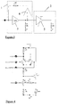
- Figure 3 illustrates an improved voltage amplifier arrangement which is suitable for use in low noise RF applications and which offers Automatic Gain Control (AGC) and low power consumption.
- AGC Automatic Gain Control
- the arrangement of Figure 3 comprises an input stage 1 and a variable gain stage 2.
- the input stage comprises a transconductance amplifier 3 having a transconductance of -gm.
- the transconductance amplifier 3 drives a load R1, and thus the voltage gain of the input stage 1 is -gmR1.
- the output of the transconducance amplifier 3 is applied to the input of a unity gain buffer amplifier 4 connected in a feedback loop.
- the output of the buffer amplifier 4 drives a feedback resistance Rf as well as the input to an AGC amplifier 5 of the variable gain stage 2.
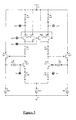
- FIG 4 illustrates a detailed circuit implementing the amplifier arrangement of Figure 3.
- the voltage Vout developed across the resistance R1 is buffered via the emitter follower transistor Q1 and is fed back via resistance Rf to determine the input impedance Rin.
- the resistor R1 connected to the collector of Q0 is also connected to the emitters of transistors Q2 and Q3.
- Transistors Q2 and Q3 receive at their bases +ve and -ve AGC signals respectively. Under maximum AGC, transistor Q3 is effectively off.
- this current is the same as the signal current emerging from the collector of transistor Q0.
- the AGC signal applied to the bases of transistors Q2 and Q3 some of the signal current will be steered into vcc as Q3 turns on more strongly, thus reducing the voltage gain of the amplifier arrangement.
- the input impedance of the arrangement is also set. Therefore, the combination of the shunt feedback and common base loaded output results in a low noise amplifier with AGC, without burning any unnecessary power.
- the amplifier arrangement illustrated in Figure 4 can be extended to a full differential version as shown in Figure 5.
- Transistors Qt1 and Qt2, resistances Rtl and Rt2, and the current source I3 together form the main long tail pair transconductance amplifier.
- the inputs are fed via the in+ and in- input ports.
- the output of the long tail pair amplifier feeds into load resistances Rt3 and Rt4 which convert the current output into a voltage output.
- the voltage output is in turn fed back through transistors Qe1 and Qe2, and resistances Rfl and Rf2 respectively, in a negative feedback fashion.
- This arrangement provides a long tail pair LNA with a controlled input impedance.
- the output of the LNA is obtained by connecting the load resistors Rt3 and Rt4 to the emitters of the current steering pairs Qt3, Qt4, and Qt5, Qt6 respectively. Hence the output of the LNA is now converted back into a current which can then be steered either fully into the final load resistors Rt5 and Rt6 or conversely into vcc, by appropriate adjustment of the agc+ and agc- inputs
- circuits illustrated in Figures 4 and 5 utilise bipolar junction transistors, and in particular npn bipolar junction transistors.
- the invention may be implemented using pnp bipolar junction transistors or a combination of npn and pnp bipolar junction transistors, or using alternative transistor structures including, but not limited to, NMOS, FETs, and GaAs MESFETs.
Landscapes
- Amplifiers (AREA)
Applications Claiming Priority (2)
| Application Number | Priority Date | Filing Date | Title |
|---|---|---|---|
| GB0001539 | 2000-01-22 | ||
| GB0001539A GB2358532A (en) | 2000-01-22 | 2000-01-22 | AC voltage amplifier using current mode stages |
Publications (3)
| Publication Number | Publication Date |
|---|---|
| EP1119100A2 true EP1119100A2 (fr) | 2001-07-25 |
| EP1119100A3 EP1119100A3 (fr) | 2003-10-29 |
| EP1119100B1 EP1119100B1 (fr) | 2006-09-06 |
Family
ID=9884203
Family Applications (1)
| Application Number | Title | Priority Date | Filing Date |
|---|---|---|---|
| EP00309862A Expired - Lifetime EP1119100B1 (fr) | 2000-01-22 | 2000-11-06 | Amplificateurs |
Country Status (4)
| Country | Link |
|---|---|
| US (1) | US6480066B1 (fr) |
| EP (1) | EP1119100B1 (fr) |
| JP (1) | JP2001203544A (fr) |
| GB (1) | GB2358532A (fr) |
Cited By (2)
| Publication number | Priority date | Publication date | Assignee | Title |
|---|---|---|---|---|
| EP1359666A2 (fr) * | 2002-05-03 | 2003-11-05 | Zarlink Semiconductor Limited | Etage de traitement du signal et circuit d'accord haute fréquence |
| WO2004021562A2 (fr) * | 2002-08-30 | 2004-03-11 | Microtune (Texas), L.P. | Systeme et procede pour determiner l'impedance d'entree d'un amplificateur dans une configuration empilee |
Families Citing this family (10)
| Publication number | Priority date | Publication date | Assignee | Title |
|---|---|---|---|---|
| US6711391B1 (en) * | 2000-10-10 | 2004-03-23 | Qualcomm, Incorporated | Gain linearizer for variable gain amplifiers |
| US7054605B1 (en) * | 2001-01-16 | 2006-05-30 | Sequoia Communications Corporation | Variable-gain low noise amplifier to reduce linearity requirements on a radio receiver |
| US6570448B1 (en) * | 2002-01-23 | 2003-05-27 | Broadcom Corporation | System and method for a startup circuit for a differential CMOS amplifier |
| US6888406B2 (en) * | 2002-08-12 | 2005-05-03 | Microtune (Texas), L.P. | Highly linear variable gain amplifier |
| US7180369B1 (en) * | 2003-05-15 | 2007-02-20 | Marvell International Ltd. | Baseband filter start-up circuit |
| US7259626B2 (en) * | 2004-12-28 | 2007-08-21 | Broadcom Corporation | Apparatus and method for biasing cascode devices in a differential pair using the input, output, or other nodes in the circuit |
| US7355466B2 (en) * | 2006-01-26 | 2008-04-08 | Honeywell International Inc. | Passive mixer with direct current bias |
| JP2009065511A (ja) * | 2007-09-07 | 2009-03-26 | Fujitsu Ltd | 増幅回路及び通信機 |
| TWI378640B (en) * | 2009-10-23 | 2012-12-01 | Sunplus Technology Co Ltd | Variable-gain low noise amplifier |
| CN111969957B (zh) * | 2020-08-13 | 2022-06-21 | 西安博瑞集信电子科技有限公司 | 一种跨导放大电路及混频器 |
Citations (3)
| Publication number | Priority date | Publication date | Assignee | Title |
|---|---|---|---|---|
| US3891935A (en) * | 1973-09-21 | 1975-06-24 | Rca Corp | Transistor biasing arrangement |
| EP0397240A1 (fr) * | 1989-05-08 | 1990-11-14 | Koninklijke Philips Electronics N.V. | Circuit amplificateur |
| US5751190A (en) * | 1996-08-22 | 1998-05-12 | Northern Telecom Limited | Gain-controlled amplifier and distributed amplifier |
Family Cites Families (13)
| Publication number | Priority date | Publication date | Assignee | Title |
|---|---|---|---|---|
| IT1212776B (it) * | 1983-09-29 | 1989-11-30 | Ates Componenti Elettron | Stadio d'ingresso amplificatore e miscelatore a transistori per un radioricevitore. |
| US4553108A (en) * | 1983-11-09 | 1985-11-12 | Rockwell International Corporation | Low noise feedback amplifier |
| EP0549045B1 (fr) * | 1991-12-23 | 1996-11-27 | Laboratoires D'electronique Philips S.A.S. | Dispositif semiconducteur comprenant un amplificateur différentiel à deux étages |
| GB2272122B (en) * | 1992-10-28 | 1996-07-17 | Plessey Semiconductors Ltd | Wideband constant impedance amplifiers |
| US5552742A (en) * | 1995-02-13 | 1996-09-03 | Motorola, Inc. | Circuit for controlling current flow between two nodes |
| GB9519233D0 (en) * | 1995-09-20 | 1995-11-22 | Plessey Semiconductors Ltd | Amplifier arrangements |
| DE69529908T2 (de) * | 1995-11-30 | 2003-12-04 | Stmicroelectronics S.R.L., Agrate Brianza | Frequenzselbstkompensierter Operationsverstärker |
| US5668468A (en) * | 1996-01-11 | 1997-09-16 | Harris Corporation | Common mode stabilizing circuit and method |
| JPH10173456A (ja) * | 1996-12-11 | 1998-06-26 | Fujitsu Ltd | 信号増幅回路 |
| US6040731A (en) * | 1997-05-01 | 2000-03-21 | Raytheon Company | Differential pair gain control stage |
| US6049251A (en) * | 1998-03-30 | 2000-04-11 | Maxim Integrated Products, Inc. | Wide-dynamic-range variable-gain amplifier |
| US6147559A (en) * | 1998-07-30 | 2000-11-14 | Philips Electronics North America Corporation | Noise figure and linearity improvement technique using shunt feedback |
| US6211737B1 (en) * | 1999-07-16 | 2001-04-03 | Philips Electronics North America Corporation | Variable gain amplifier with improved linearity |
-
2000
- 2000-01-22 GB GB0001539A patent/GB2358532A/en not_active Withdrawn
- 2000-11-02 US US09/705,499 patent/US6480066B1/en not_active Expired - Lifetime
- 2000-11-06 EP EP00309862A patent/EP1119100B1/fr not_active Expired - Lifetime
- 2000-12-07 JP JP2000373017A patent/JP2001203544A/ja active Pending
Patent Citations (3)
| Publication number | Priority date | Publication date | Assignee | Title |
|---|---|---|---|---|
| US3891935A (en) * | 1973-09-21 | 1975-06-24 | Rca Corp | Transistor biasing arrangement |
| EP0397240A1 (fr) * | 1989-05-08 | 1990-11-14 | Koninklijke Philips Electronics N.V. | Circuit amplificateur |
| US5751190A (en) * | 1996-08-22 | 1998-05-12 | Northern Telecom Limited | Gain-controlled amplifier and distributed amplifier |
Non-Patent Citations (1)
| Title |
|---|
| HARVEY B ED - JOPKE J V: "A wideband current-mode variable gain-control circuit" BIPOLAR CIRCUITS AND TECHNOLOGY MEETING, 1991., PROCEEDINGS OF THE 1991 MINNEAPOLIS, MN, USA 9-10 SEPT. 1991, NEW YORK, NY, USA,IEEE, US, 9 September 1991 (1991-09-09), pages 233-240, XP010048592 ISBN: 0-7803-0103-X * |
Cited By (4)
| Publication number | Priority date | Publication date | Assignee | Title |
|---|---|---|---|---|
| EP1359666A2 (fr) * | 2002-05-03 | 2003-11-05 | Zarlink Semiconductor Limited | Etage de traitement du signal et circuit d'accord haute fréquence |
| EP1359666A3 (fr) * | 2002-05-03 | 2003-11-19 | Zarlink Semiconductor Limited | Etage de traitement du signal et circuit d'accord haute fréquence |
| WO2004021562A2 (fr) * | 2002-08-30 | 2004-03-11 | Microtune (Texas), L.P. | Systeme et procede pour determiner l'impedance d'entree d'un amplificateur dans une configuration empilee |
| WO2004021562A3 (fr) * | 2002-08-30 | 2004-07-29 | Microtune Texas Lp | Systeme et procede pour determiner l'impedance d'entree d'un amplificateur dans une configuration empilee |
Also Published As
| Publication number | Publication date |
|---|---|
| EP1119100A3 (fr) | 2003-10-29 |
| GB0001539D0 (en) | 2000-03-15 |
| GB2358532A (en) | 2001-07-25 |
| US6480066B1 (en) | 2002-11-12 |
| EP1119100B1 (fr) | 2006-09-06 |
| JP2001203544A (ja) | 2001-07-27 |
Similar Documents
| Publication | Publication Date | Title |
|---|---|---|
| US4227256A (en) | AM Broadcast tuner with automatic gain control | |
| US6744319B2 (en) | Exponential function generator embodied by using a CMOS process and variable gain amplifier employing the same | |
| US6175274B1 (en) | Switched gain low noise amplifier | |
| JPH0414525B2 (fr) | ||
| EP1119100A2 (fr) | Amplificateurs | |
| US6304142B1 (en) | Variable transconductance amplifier | |
| US4406990A (en) | Direct coupled DC amplification circuit | |
| EP0342671A2 (fr) | Circuit de contrôle automatique de gain retardé sous forme d'un circuit intégré | |
| US4274060A (en) | Signal change-over amplifier | |
| US4433303A (en) | Push-pull amplifier circuit with field-effect transistors | |
| US4864248A (en) | Amplifier arrangement with controllable gain | |
| US6972624B1 (en) | Low-voltage high dynamic range variable-gain amplifier | |
| US5382919A (en) | Wideband constant impedance amplifiers | |
| JPS5844803A (ja) | 11/2ポ−ルオ−デイオ電力増幅器 | |
| KR100573348B1 (ko) | 신호 처리단 및 무선 주파수 튜너 | |
| US8115552B2 (en) | Amplifier circuit with step gain | |
| US4366443A (en) | Television intermediate frequency amplifier | |
| JP2649223B2 (ja) | Uhf増幅混合回路 | |
| US6407632B1 (en) | Radio frequency amplifier | |
| JP3170824B2 (ja) | オーディオ電力増幅器 | |
| US6995610B2 (en) | Amplifier and radio frequency tuner | |
| EP1049249A1 (fr) | Amplificateur à gain variable | |
| US4918400A (en) | Amplifier circuit | |
| JPH021945Y2 (fr) | ||
| SU970635A1 (ru) | Двухтактный усилитель |
Legal Events
| Date | Code | Title | Description |
|---|---|---|---|
| PUAI | Public reference made under article 153(3) epc to a published international application that has entered the european phase |
Free format text: ORIGINAL CODE: 0009012 |
|
| AK | Designated contracting states |
Kind code of ref document: A2 Designated state(s): AT BE CH CY DE DK ES FI FR GB GR IE IT LI LU MC NL PT SE TR |
|
| AX | Request for extension of the european patent |
Free format text: AL;LT;LV;MK;RO;SI |
|
| RAP1 | Party data changed (applicant data changed or rights of an application transferred) |
Owner name: ZARLINK SEMICONDUCTOR LIMITED |
|
| PUAL | Search report despatched |
Free format text: ORIGINAL CODE: 0009013 |
|
| AK | Designated contracting states |
Kind code of ref document: A3 Designated state(s): AT BE CH CY DE DK ES FI FR GB GR IE IT LI LU MC NL PT SE TR |
|
| AX | Request for extension of the european patent |
Extension state: AL LT LV MK RO SI |
|
| RIC1 | Information provided on ipc code assigned before grant |
Ipc: 7H 03F 1/30 B Ipc: 7H 03F 1/22 B Ipc: 7H 03G 1/00 A |
|
| 17P | Request for examination filed |
Effective date: 20031105 |
|
| AKX | Designation fees paid |
Designated state(s): DE |
|
| 17Q | First examination report despatched |
Effective date: 20040609 |
|
| RBV | Designated contracting states (corrected) |
Designated state(s): GB |
|
| REG | Reference to a national code |
Ref country code: DE Ref legal event code: 8566 |
|
| GRAP | Despatch of communication of intention to grant a patent |
Free format text: ORIGINAL CODE: EPIDOSNIGR1 |
|
| GRAS | Grant fee paid |
Free format text: ORIGINAL CODE: EPIDOSNIGR3 |
|
| GRAA | (expected) grant |
Free format text: ORIGINAL CODE: 0009210 |
|
| AK | Designated contracting states |
Kind code of ref document: B1 Designated state(s): GB |
|
| REG | Reference to a national code |
Ref country code: GB Ref legal event code: FG4D |
|
| PGFP | Annual fee paid to national office [announced via postgrant information from national office to epo] |
Ref country code: GB Payment date: 20061101 Year of fee payment: 7 |
|
| REG | Reference to a national code |
Ref country code: GB Ref legal event code: 732E |
|
| PLBE | No opposition filed within time limit |
Free format text: ORIGINAL CODE: 0009261 |
|
| STAA | Information on the status of an ep patent application or granted ep patent |
Free format text: STATUS: NO OPPOSITION FILED WITHIN TIME LIMIT |
|
| 26N | No opposition filed |
Effective date: 20070607 |
|
| REG | Reference to a national code |
Ref country code: HK Ref legal event code: WD Ref document number: 1038445 Country of ref document: HK |
|
| GBPC | Gb: european patent ceased through non-payment of renewal fee |
Effective date: 20071106 |
|
| PG25 | Lapsed in a contracting state [announced via postgrant information from national office to epo] |
Ref country code: GB Free format text: LAPSE BECAUSE OF NON-PAYMENT OF DUE FEES Effective date: 20071106 |