EP1118924B1 - Procédé de fonctionnement et système à microprocesseur - Google Patents
Procédé de fonctionnement et système à microprocesseur Download PDFInfo
- Publication number
- EP1118924B1 EP1118924B1 EP00100994.3A EP00100994A EP1118924B1 EP 1118924 B1 EP1118924 B1 EP 1118924B1 EP 00100994 A EP00100994 A EP 00100994A EP 1118924 B1 EP1118924 B1 EP 1118924B1
- Authority
- EP
- European Patent Office
- Prior art keywords
- unit
- bus
- lines
- signal
- access
- Prior art date
- Legal status (The legal status is an assumption and is not a legal conclusion. Google has not performed a legal analysis and makes no representation as to the accuracy of the status listed.)
- Expired - Lifetime
Links
Images
Classifications
-
- G—PHYSICS
- G06—COMPUTING OR CALCULATING; COUNTING
- G06K—GRAPHICAL DATA READING; PRESENTATION OF DATA; RECORD CARRIERS; HANDLING RECORD CARRIERS
- G06K19/00—Record carriers for use with machines and with at least a part designed to carry digital markings
- G06K19/06—Record carriers for use with machines and with at least a part designed to carry digital markings characterised by the kind of the digital marking, e.g. shape, nature, code
- G06K19/067—Record carriers with conductive marks, printed circuits or semiconductor circuit elements, e.g. credit or identity cards also with resonating or responding marks without active components
- G06K19/07—Record carriers with conductive marks, printed circuits or semiconductor circuit elements, e.g. credit or identity cards also with resonating or responding marks without active components with integrated circuit chips
- G06K19/073—Special arrangements for circuits, e.g. for protecting identification code in memory
-
- G—PHYSICS
- G06—COMPUTING OR CALCULATING; COUNTING
- G06F—ELECTRIC DIGITAL DATA PROCESSING
- G06F21/00—Security arrangements for protecting computers, components thereof, programs or data against unauthorised activity
- G06F21/70—Protecting specific internal or peripheral components, in which the protection of a component leads to protection of the entire computer
- G06F21/71—Protecting specific internal or peripheral components, in which the protection of a component leads to protection of the entire computer to assure secure computing or processing of information
- G06F21/75—Protecting specific internal or peripheral components, in which the protection of a component leads to protection of the entire computer to assure secure computing or processing of information by inhibiting the analysis of circuitry or operation
- G06F21/755—Protecting specific internal or peripheral components, in which the protection of a component leads to protection of the entire computer to assure secure computing or processing of information by inhibiting the analysis of circuitry or operation with measures against power attack
-
- G—PHYSICS
- G06—COMPUTING OR CALCULATING; COUNTING
- G06K—GRAPHICAL DATA READING; PRESENTATION OF DATA; RECORD CARRIERS; HANDLING RECORD CARRIERS
- G06K19/00—Record carriers for use with machines and with at least a part designed to carry digital markings
- G06K19/06—Record carriers for use with machines and with at least a part designed to carry digital markings characterised by the kind of the digital marking, e.g. shape, nature, code
- G06K19/067—Record carriers with conductive marks, printed circuits or semiconductor circuit elements, e.g. credit or identity cards also with resonating or responding marks without active components
- G06K19/07—Record carriers with conductive marks, printed circuits or semiconductor circuit elements, e.g. credit or identity cards also with resonating or responding marks without active components with integrated circuit chips
- G06K19/073—Special arrangements for circuits, e.g. for protecting identification code in memory
- G06K19/07309—Means for preventing undesired reading or writing from or onto record carriers
- G06K19/07363—Means for preventing undesired reading or writing from or onto record carriers by preventing analysis of the circuit, e.g. dynamic or static power analysis or current analysis
-
- G—PHYSICS
- G06—COMPUTING OR CALCULATING; COUNTING
- G06F—ELECTRIC DIGITAL DATA PROCESSING
- G06F12/00—Accessing, addressing or allocating within memory systems or architectures
- G06F12/14—Protection against unauthorised use of memory or access to memory
- G06F12/1408—Protection against unauthorised use of memory or access to memory by using cryptography
-
- G—PHYSICS
- G06—COMPUTING OR CALCULATING; COUNTING
- G06F—ELECTRIC DIGITAL DATA PROCESSING
- G06F2207/00—Indexing scheme relating to methods or arrangements for processing data by operating upon the order or content of the data handled
- G06F2207/72—Indexing scheme relating to groups G06F7/72 - G06F7/729
- G06F2207/7219—Countermeasures against side channel or fault attacks
-
- G—PHYSICS
- G06—COMPUTING OR CALCULATING; COUNTING
- G06F—ELECTRIC DIGITAL DATA PROCESSING
- G06F2221/00—Indexing scheme relating to security arrangements for protecting computers, components thereof, programs or data against unauthorised activity
- G06F2221/21—Indexing scheme relating to G06F21/00 and subgroups addressing additional information or applications relating to security arrangements for protecting computers, components thereof, programs or data against unauthorised activity
- G06F2221/2123—Dummy operation
Definitions
- the invention relates to a method for operating a microprocessor arrangement having a first and a further unit, a bus via which these units are connected to each other with a line for a status signal and lines for further bus signals and a bus control unit for controlling accesses of the first unit to the another unit. Moreover, the invention relates to a microprocessor arrangement which is suitable for carrying out the method.
- Microprocessor arrangements include besides the central processing and control unit (CPU) further units such as memory or peripheral units for signal input and signal output integrated on a single chip, so-called microcontroller.
- CPU central processing and control unit
- microcontrollers can be used in security-relevant systems, for example chip cards.
- the microcontroller serves to encrypt the data traffic between a reader and the chip card, to check access permissions and to perform other secret operations.
- timing of the current consumed by the microcontroller can be used to spy on the function of the microcontroller. For example, trigger points can be obtained from the current profile in order to control subsequent measurements in the correct time; or conclusions can be drawn about the specific type of calculation and encryption / decryption algorithms used in the processor; or even parts of the processed payload be determined.
- Bus accesses in particular generate a characteristic current profile because they run according to a defined signal protocol and the switching operations provide a clear current profile due to the high capacitive loads to be driven. The application of conventional microcontrollers in safety-critical applications is therefore problematic.
- Dallas Semiconductor Corp: Section 1: Introduction, October 6, 1993, "Data Book Soft Microcontroller” shows that in a random sequence, a dummy cycle is inserted on the bus instead of a real cycle.
- a dummy cycle does not include any real data, but only randomly generated data in order to increase the security against eavesdropping of the bus system.
- the dummy data are applied in a randomly changing sequence of dummy cycles with real cycles on lines for the bus signals.
- Such a method allows the obfuscation or camouflage of real data with dummy data and thus increases the security against spying out the transmitted data, but also increases the time duration of the data transmission of a data packet via the bus system.
- the object of the invention is to provide a method for operating a microprocessor arrangement that is tap-proof, and which is improved over the prior art.
- a further object is to specify a microprocessor arrangement suitable for carrying out the method.
- the object concerning the method is solved by a method for operating a microprocessor arrangement having a first unit and a further unit; a bus via which the first unit is connected to the further unit and which comprises a line for a status signal indicating the operating state of the bus and lines for further bus signals indicating a data value; a bus control unit for controlling accesses of the first unit to the further unit via the bus; in which method, when the bus control unit notifies, via the line for the status signal, that no access is made from the first unit to the further unit, a data value is randomly generated and applied to the lines for the further bus signals.
- a microprocessor arrangement for carrying out the method according to the invention comprises: a first unit and a further unit; a bus via which the first unit is connected to the further unit and which comprises a line for a status signal indicating the operating state of the bus and lines for further bus signals indicating a data value; a bus control unit for controlling accesses of the first unit to the further unit via the bus; a random number generator connectable to the lines for the further bus signals when the status signal indicates that no access is to be made from the first unit to the further unit.
- the bus status signal indicates for which task the bus is currently being used by the central processing and control unit (CPU). If the bus is currently in the idle state in the considered clock section, no valid signals are present on the bus data lines of the bus. According to the invention, a randomly generated signal is then transmitted over the data lines of the bus. This will the current profile changes randomly. The current profile is thus disguised in relation to the transmitted over the bus payload, so that conclusions about the payload due to a statistical evaluation of the current profile significantly more difficult or even impossible.
- CPU central processing and control unit
- the bus state signal indicates the state of the bus lines one clock in advance. It is also possible that the bus state signal indicates the state of the remaining bus lines in the same clock.
- the units that can be controlled by the CPU are assigned addresses.
- an address assigned to a memory or a peripheral unit this means that the memory and a memory cell or the corresponding peripheral unit contained therein are to be activated in order to receive data from the bus or to output data to the bus.
- an address is nevertheless output on the bus.
- this address is not an address assigned to a unit connected to the bus, but any other address. This has the consequence that none of the connected units is activated. Nevertheless, however, this arbitrary address is transmitted via the bus, thereby generating a corresponding current profile. This address is generated randomly. The current profile is accordingly changed randomly. It is to ensure that the random number does not match a valid address of a unit connected to the bus.
- the data value output on the bus in this way contains the meaning of an address by the respective state of the bus state signal.
- the bus state signal also indicates that either an address is output on the data lines of the bus or a data is output (written) to the addressed unit.
- the same signal lines of the bus can be used. This is called a multiplexed data / address bus.
- the term data value is to be understood generally and includes data values that represent an address or data or program data to be processed, etc.
- a random value is transmitted in the following cycle. If an address is transmitted for which there is no unit connected to the bus, random values are transmitted in the subsequent operation cycles until an existing unit is addressed again by a valid address. In previous microprocessors, an address that was not assigned to a connected unit represented a programming error. In the invention, however, the transmission of such a random address should be understood as meaning that access to a nonexistent destination is performed to accommodate the otherwise unused bus cycles disguise.
- the bus of the microprocessor arrangement may additionally comprise a line for an enable signal, which is led to the other units connected to the bus.
- the enable signal conveys to these units access via the bus.
- the release line is suitably controlled by a signaled by the bus state signal idle state with random values.
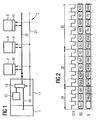
- the microcontroller shown has a central control and processing unit (CPU) 1, by means of which the internal operating sequences, in particular the accesses to the bus 2, are controlled.
- the CPU 1 comprises a bus control unit 11.
- the bus itself comprises at least one signal line 21, which indicates the bus state, and a plurality of lines 22, via which both addresses of connected units and data values are successively transmitted, so-called multiplexed data / address bus.
- Connected to the bus 2 is a memory 3 in which data values to be processed and / or program instructions are stored.
- a first peripheral unit 4 is provided as well as a second peripheral unit 5, via which data are exchanged with functional units connected to the outside of the chip.
- the microcontroller is used in a smart card to communicate with a reader.
- Each of the units 3, 4, 5 connected to the bus has a bus interface 31, 41 and 51, respectively.
- the bus control unit 11 and the interfaces 31, 41, 51 work together in master-slave dependency.
- the bus control unit runs the data lines 22 output a sequence of randomly generated data values.
- a random number generator 12 which is connected via a multiplexer 13 to the data lines 22 of the bus.
- the multiplexer 13 switches over to the other terminal 14, which forwards the transmitted or received data to the other functional units of the CPU 1.
- the bus state signal BS transmitted on the line 21 is in FIG. 2 together with the data values B transmitted on the data / address lines 22.
- the bus is clocked so that respective signal states are valid for one clock period of the clock CLK.
- the bus state signal BS may be the idle state IDLE, the address transfer state ADR, the write WR write state in which a data is transferred from the CPU 1 to one of the units 3, 4, 5, and a state RD for a read operation, in which a data value from one of the units 3, 4, 5 is read out and transmitted to the CPU 1 occupy.
- the bus is controlled such that the state of the signal BS in a first clock indicates the state that the data values of the data / address lines B occupy in the next following clock. This means that the data values transmitted via the address / data lines 22 correspond to the state of the bus state signal BS which has been directly transmitted one clock previously.
- the first three clocks 31 show the signal flow in a write access to the memory 3.
- the bus In the first clock, the bus is in the idle state, wherein the bus state signal BS assumes the signal value IDLE.
- the bus state signal BS In the subsequent operating cycle is transmitted via the data / address lines 22 randomly generated by the random number generator 12 data RNG.
- the bus state signal BS is switched by the bus master 11 to the address transfer state ADR. This means for the data / address signal lines 22 of the bus, that a valid address MEM of a memory cell contained in the memory 3 is transmitted.
- the bus state signal BS signals a write WR.
- the bus lines 22 then carry the data DATA to be stored in the memory 3 to the memory cell with the address MEM previously specified in the clock.
- the state IDLE is first transmitted for one clock for the bus state signal BS.
- a random data RNG is output in the immediately following clock.
- the bus state signal BS signals the transmission of an address by the state ADR.
- a data value NON is then transmitted which does not correspond to any of the addresses in the address space of the units 3, 4 and 5.
- the data value NON is randomly generated in the random number generator 12. From a programming point of view, this means that a unit with the address NON is addressed, which does not exist in real hardware.
- the bus state signal BS assumes the signal states RD, WR and RD.
- random numbers RNG generated by the random number generator 12 are transmitted. In practice, there may be far more than just the three clock sections shown by way of example with the transmission of random number values on the address / data signal lines.
- the bus state signal BS is in turn switched to an idle state IDLE, wherein on the address / data lines, a random value RNG is transmitted. Subsequently, a write access to the peripheral unit 4 with the address P1 and a read access to the peripheral unit 5 with the address P2.
Landscapes
- Engineering & Computer Science (AREA)
- Computer Hardware Design (AREA)
- Physics & Mathematics (AREA)
- Theoretical Computer Science (AREA)
- Computer Security & Cryptography (AREA)
- General Engineering & Computer Science (AREA)
- General Physics & Mathematics (AREA)
- Microelectronics & Electronic Packaging (AREA)
- Mathematical Physics (AREA)
- Software Systems (AREA)
- Microcomputers (AREA)
- Bus Control (AREA)
Claims (8)
- Procédé pour faire fonctionner un système à microprocesseur comprenant- une première unité (1) et une autre unité (3, 4, 5),- un bus (2), par lequel la première unité (1) est reliée à l'autre unité (3, 4, 5) et qui comprend des lignes (22) pour des signaux (B) de bus, qui indiquent une valeur de données,- une unité (11) de commande de bus pour la commande d'accès de la première unité (1) à l'autre unité (3, 4, 5) par l'intermédiaire du bus (2),caractérisé par- une ligne (21) pour un signal d'état, qui indique l'état de fonctionnement du bus (2),- dans lequel, lorsqu'il est fait part, par l'unité (11) de commande de bus par l'intermédiaire de la ligne (21) pour le signal (BS) d'état, qu'un accès n'est pas effectué par la première unité (1) à l'autre unité (3, 4, 5), une valeur de données est produite d'une manière commandée aléatoirement et est créée sur les lignes (22) pour les autres signaux (B) de bus.
- Procédé suivant la revendication 1,
caractérisé en ce que
l'unité (11) de commande de bus produit en cadence le signal d'état et la valeur (B) de données et en ce que, lorsqu'il est fait part dans une première cadence qu'un accès n'a pas été effectué par la première unité (1) à l'autre unité (3, 4, 5), dans une cadence suivante la valeur de données produite d'une manière commandée aléatoirement est produite et est créée sur les lignes (22) pour les autres signaux (B) de bus. - Procédé suivant la revendication 2,
caractérisé en ce que
il est affecté à l'autre unité (3) du système à microprocesseur une adresse, par laquelle il peut être accédé par la première unité (1) à l'autre unité (3), en ce que, dans la cadence suivant une première cadence, dans laquelle il est fait part qu'un accès n'a pas été effectué par la première unité à l'autre unité, une autre adresse que celle affectée à l'autre unité est créée sur les lignes (22) pour les signaux (B) de bus. - Procédé suivant la revendication 3,
caractérisé en ce que
dans une cadence suivant à nouveau la cadence suivante, un accès en lecture ou un accès en écriture est réalisé par l'intermédiaire du bus (2). - Procédé suivant la revendication 4,
caractérisé en ce que
le signal d'état comprend des états de signal pour un accès en lecture et pour un accès en écriture et en ce qu'il est créé, sur la ligne (21) pour le signal d'état, l'un de ces états de signal et en ce qu'il est créé, affectée aux lignes (22) pour les autres signaux (B) de bus, une valeur de données produite d'une manière commandée aléatoirement. - Procédé suivant la revendication 5,
caractérisé en ce que
le bus (2) du système à microprocesseur comprend une ligne pour un signal de libération de l'autre unité et en ce que, lorsqu'il est fait part, par l'unité de commande de bus par l'intermédiaire de la ligne pour le signal d'état, qu'un accès n'a pas été effectué par la première unité à l'autre unité, il est créé sur la ligne pour le signal de libération un signal produit de manière commandée aléatoirement. - Système à microprocesseur pour effectue le procédé suivant l'une des revendications 1 à 6, qui comprend :- une première unité (1) et une autre unité (3, 4, 5),- un bus (2), par lequel la première unité (1) est reliée à l'autre unité (3, 4, 5) et qui est prévu pour comprendre les lignes (22) pour d'autres signaux (B) de bus, qui indiquent une valeur de données,- une unité (11) de commande de bus pour la commande d'accès de la première unité (1) à l'autre unité (3, 4, 5) par l'intermédiaire du bus (2)caractérisé par- une ligne (21) pour un signal d'état, qui indique l'état de fonctionnement du bus,- un générateur (12) aléatoire, qui, lorsqu'il est fait part, par l'unité (11) de commande de bus par l'intermédiaire de la ligne (21) pour le signal (BS) d'état, qu'un accès n'a pas été effectué par la première unité (1) à l'autre unité (3, 4, 5), produit d'une manière commandée aléatoirement une valeur de données et l'applique aux lignes (22) pour les autres signaux (B) de bus.
- Système à microprocesseur suivant la revendication 7, caractérisé en ce que
la première unité (1) est une unité de traitement et de commande d'un microprocesseur et en ce que l'autre unité est une unité (4, 5) périphérique d'un microprocesseur d'entrée de signaux à un microprocesseur et de sortie de signaux d'un microprocesseur ou une mémoire.
Priority Applications (5)
| Application Number | Priority Date | Filing Date | Title |
|---|---|---|---|
| EP00100994.3A EP1118924B1 (fr) | 2000-01-19 | 2000-01-19 | Procédé de fonctionnement et système à microprocesseur |
| CNB01803750XA CN1249549C (zh) | 2000-01-19 | 2001-01-16 | 微处理器阵列装置操作方法 |
| PCT/DE2001/000155 WO2001053930A2 (fr) | 2000-01-19 | 2001-01-16 | Procede pour actionner un systeme de microprocesseurs et systeme de microprocesseurs correspondant |
| JP2001554158A JP2003521033A (ja) | 2000-01-19 | 2001-01-16 | マイクロプロセッサシステムを動作する方法および対応するマイクロプロセッサシステム |
| US10/199,589 US7020730B2 (en) | 2000-01-19 | 2002-07-19 | Method for operating a microprocessor configuration and microprocessor configuration |
Applications Claiming Priority (1)
| Application Number | Priority Date | Filing Date | Title |
|---|---|---|---|
| EP00100994.3A EP1118924B1 (fr) | 2000-01-19 | 2000-01-19 | Procédé de fonctionnement et système à microprocesseur |
Publications (2)
| Publication Number | Publication Date |
|---|---|
| EP1118924A1 EP1118924A1 (fr) | 2001-07-25 |
| EP1118924B1 true EP1118924B1 (fr) | 2016-07-20 |
Family
ID=8167658
Family Applications (1)
| Application Number | Title | Priority Date | Filing Date |
|---|---|---|---|
| EP00100994.3A Expired - Lifetime EP1118924B1 (fr) | 2000-01-19 | 2000-01-19 | Procédé de fonctionnement et système à microprocesseur |
Country Status (5)
| Country | Link |
|---|---|
| US (1) | US7020730B2 (fr) |
| EP (1) | EP1118924B1 (fr) |
| JP (1) | JP2003521033A (fr) |
| CN (1) | CN1249549C (fr) |
| WO (1) | WO2001053930A2 (fr) |
Families Citing this family (6)
| Publication number | Priority date | Publication date | Assignee | Title |
|---|---|---|---|---|
| FR2808360B1 (fr) * | 2000-04-28 | 2002-06-28 | Gemplus Card Int | Procede de contre mesure dans un microcircuit mettant en oeuvre le procede et carte a puce comportant ledit microcircuit |
| EP1496420B1 (fr) | 2000-05-22 | 2007-07-04 | Infineon Technologies AG | Unité de traitement de données et méthode associée |
| US6515304B1 (en) | 2000-06-23 | 2003-02-04 | International Business Machines Corporation | Device for defeating reverse engineering of integrated circuits by optical means |
| US6798567B2 (en) * | 2002-03-07 | 2004-09-28 | Lucent Technologies Inc. | Method and apparatus for controlling power transients in an optical communication system |
| US8635467B2 (en) | 2011-10-27 | 2014-01-21 | Certicom Corp. | Integrated circuit with logic circuitry and multiple concealing circuits |
| US8334705B1 (en) | 2011-10-27 | 2012-12-18 | Certicom Corp. | Analog circuitry to conceal activity of logic circuitry |
Family Cites Families (12)
| Publication number | Priority date | Publication date | Assignee | Title |
|---|---|---|---|---|
| NL8201847A (nl) * | 1982-05-06 | 1983-12-01 | Philips Nv | Inrichting voor het beschermen tegen onbevoegd uitlezen van in een geheugen te memoriseren programmawoorden. |
| US5341423A (en) * | 1987-02-06 | 1994-08-23 | General Electric Company | Masked data transmission system |
| US5297201A (en) * | 1992-10-13 | 1994-03-22 | J.D. Technologies, Inc. | System for preventing remote detection of computer data from tempest signal emissions |
| US5754647A (en) * | 1996-03-27 | 1998-05-19 | United Microelectronics Corporation | Software protection apparatus and the method of protection utilizing read-write memory means having inconsistent input and output data |
| EP2280502B1 (fr) * | 1998-06-03 | 2018-05-02 | Cryptography Research, Inc. | Utilisation d'informations imprévisibles pour résister à la découverte de secrets par surveillance externe |
| US6401208B2 (en) * | 1998-07-17 | 2002-06-04 | Intel Corporation | Method for BIOS authentication prior to BIOS execution |
| US6385727B1 (en) * | 1998-09-25 | 2002-05-07 | Hughes Electronics Corporation | Apparatus for providing a secure processing environment |
| FR2789535B1 (fr) * | 1999-02-04 | 2001-09-28 | Bull Cp8 | Procede de securisation d'un ensemble electronique de cryptographie a cle secrete contre les attaques par analyse physique |
| US6419159B1 (en) * | 1999-06-14 | 2002-07-16 | Microsoft Corporation | Integrated circuit device with power analysis protection circuitry |
| US6633981B1 (en) * | 1999-06-18 | 2003-10-14 | Intel Corporation | Electronic system and method for controlling access through user authentication |
| US6295606B1 (en) * | 1999-07-26 | 2001-09-25 | Motorola, Inc. | Method and apparatus for preventing information leakage attacks on a microelectronic assembly |
| US6625737B1 (en) * | 2000-09-20 | 2003-09-23 | Mips Technologies Inc. | System for prediction and control of power consumption in digital system |
-
2000
- 2000-01-19 EP EP00100994.3A patent/EP1118924B1/fr not_active Expired - Lifetime
-
2001
- 2001-01-16 WO PCT/DE2001/000155 patent/WO2001053930A2/fr not_active Ceased
- 2001-01-16 JP JP2001554158A patent/JP2003521033A/ja not_active Withdrawn
- 2001-01-16 CN CNB01803750XA patent/CN1249549C/zh not_active Expired - Fee Related
-
2002
- 2002-07-19 US US10/199,589 patent/US7020730B2/en not_active Expired - Lifetime
Also Published As
| Publication number | Publication date |
|---|---|
| US20030005206A1 (en) | 2003-01-02 |
| WO2001053930A2 (fr) | 2001-07-26 |
| JP2003521033A (ja) | 2003-07-08 |
| EP1118924A1 (fr) | 2001-07-25 |
| CN1249549C (zh) | 2006-04-05 |
| WO2001053930A3 (fr) | 2001-12-06 |
| US7020730B2 (en) | 2006-03-28 |
| CN1395700A (zh) | 2003-02-05 |
Similar Documents
| Publication | Publication Date | Title |
|---|---|---|
| EP1668516B1 (fr) | Decodage et codage lors d'acces en ecriture a une memoire | |
| EP1246043B1 (fr) | Procédé de transfert de données sur un bus de données | |
| DE10164415A1 (de) | Verfahren und Anordnung zur Programmierung und Verifizierung von EEPROM-Pages sowie ein entsprechendes Computerprogrammprodukt und ein entsprechendes computerlesbares Speichermedium | |
| WO2001040950A2 (fr) | Dispositif microprocesseur a fonction de chiffrement | |
| EP1249010A1 (fr) | Circuit de microprocesseurs avec codage | |
| EP0892952B1 (fr) | Systeme de communications avec une station maitresse et au moins une station asservie | |
| DE19614237C1 (de) | Kommunikationssystem mit einer Meisterstation und mindestens einer Sklavenstation | |
| EP1496420B1 (fr) | Unité de traitement de données et méthode associée | |
| DE10319585B4 (de) | Manipulationsgeschütztes Datenverarbeitungssystem und zugehöriges Verfahren zum Manipulationsschutz | |
| EP1118924B1 (fr) | Procédé de fonctionnement et système à microprocesseur | |
| DE60128323T2 (de) | Datenverarbeitungsgerät und eine Speicherkarte mit dem Gerät | |
| DE10232348A1 (de) | Integrierte Halbleiterschaltung mit interner Busdatenübertragung und zugehöriges Datenübertragungsverfahren | |
| EP1548603B1 (fr) | Procede et dispositif de controle d'access memoire | |
| WO2009021816A1 (fr) | Procédé de communication et interface entre une puce associée et un microcontrôleur | |
| DE69128319T2 (de) | Arbeitsplatz mit Stossbetriebdatenübertragung | |
| DE69904290T2 (de) | Datenträgervorrichtung mit datenbus deren energieverbrauch unabhängig ist von den über den datenbus gesendeten daten | |
| DE10347301B4 (de) | Schaltung mit einem Bus mit mehreren Empfängern | |
| EP1046142B1 (fr) | Dispositif de traitement des donnees et son procede de fonctionnement permettant d'empecher toute analyse differentielle de consommation d'energie | |
| WO2001052069A2 (fr) | Procede d'acces a une memoire et ensemble circuit | |
| DE102016206109A1 (de) | Speicherdirektzugriffssteuereinrichtung für mindestens eine einen Arbeitsspeicher aufweisende Recheneinheit | |
| WO2002099729A2 (fr) | Circuit electronique destine a des interfaces de cartes a puces et procede de communication avec des interfaces de cartes a puces | |
| EP1397886B1 (fr) | Authentification selon un procede challenge-response | |
| DE19756885A1 (de) | Verfahren zum Austausch von Signalen zwischen über einen Bus verbundenen Modulen sowie Vorrichtung zur Durchführung des Verfahrens | |
| EP1046131A1 (fr) | Dispositif de traitement de donnees et son mode de fonctionnement permettant d'empecher une analyse differentielle de la consommation de courant | |
| DE10164174A1 (de) | Datenverarbeidungsvorrichtung |
Legal Events
| Date | Code | Title | Description |
|---|---|---|---|
| PUAI | Public reference made under article 153(3) epc to a published international application that has entered the european phase |
Free format text: ORIGINAL CODE: 0009012 |
|
| AK | Designated contracting states |
Kind code of ref document: A1 Designated state(s): AT BE CH CY DE DK ES FI FR GB GR IE IT LI LU MC NL PT SE |
|
| AX | Request for extension of the european patent |
Free format text: AL;LT;LV;MK;RO;SI |
|
| 17P | Request for examination filed |
Effective date: 20020117 |
|
| AKX | Designation fees paid |
Free format text: AT DE ES FR GB IT |
|
| 17Q | First examination report despatched |
Effective date: 20070919 |
|
| RAP1 | Party data changed (applicant data changed or rights of an application transferred) |
Owner name: INFINEON TECHNOLOGIES AG |
|
| REG | Reference to a national code |
Ref country code: DE Ref legal event code: R079 Ref document number: 50016452 Country of ref document: DE Free format text: PREVIOUS MAIN CLASS: G06F0001000000 Ipc: G06F0021750000 |
|
| GRAP | Despatch of communication of intention to grant a patent |
Free format text: ORIGINAL CODE: EPIDOSNIGR1 |
|
| RIC1 | Information provided on ipc code assigned before grant |
Ipc: G06F 21/55 20130101ALI20160127BHEP Ipc: G06K 19/073 20060101ALI20160127BHEP Ipc: G06F 12/14 20060101ALN20160127BHEP Ipc: G06F 21/75 20130101AFI20160127BHEP |
|
| INTG | Intention to grant announced |
Effective date: 20160209 |
|
| RIC1 | Information provided on ipc code assigned before grant |
Ipc: G06F 21/75 20130101AFI20160129BHEP Ipc: G06F 21/55 20130101ALI20160129BHEP Ipc: G06F 12/14 20060101ALN20160129BHEP Ipc: G06K 19/073 20060101ALI20160129BHEP |
|
| GRAS | Grant fee paid |
Free format text: ORIGINAL CODE: EPIDOSNIGR3 |
|
| GRAA | (expected) grant |
Free format text: ORIGINAL CODE: 0009210 |
|
| AK | Designated contracting states |
Kind code of ref document: B1 Designated state(s): AT DE ES FR GB IT |
|
| REG | Reference to a national code |
Ref country code: GB Ref legal event code: FG4D Free format text: NOT ENGLISH |
|
| REG | Reference to a national code |
Ref country code: AT Ref legal event code: REF Ref document number: 814613 Country of ref document: AT Kind code of ref document: T Effective date: 20160815 |
|
| REG | Reference to a national code |
Ref country code: DE Ref legal event code: R096 Ref document number: 50016452 Country of ref document: DE |
|
| REG | Reference to a national code |
Ref country code: FR Ref legal event code: PLFP Year of fee payment: 18 |
|
| PG25 | Lapsed in a contracting state [announced via postgrant information from national office to epo] |
Ref country code: IT Free format text: LAPSE BECAUSE OF FAILURE TO SUBMIT A TRANSLATION OF THE DESCRIPTION OR TO PAY THE FEE WITHIN THE PRESCRIBED TIME-LIMIT Effective date: 20160720 |
|
| PG25 | Lapsed in a contracting state [announced via postgrant information from national office to epo] |
Ref country code: ES Free format text: LAPSE BECAUSE OF FAILURE TO SUBMIT A TRANSLATION OF THE DESCRIPTION OR TO PAY THE FEE WITHIN THE PRESCRIBED TIME-LIMIT Effective date: 20160720 |
|
| REG | Reference to a national code |
Ref country code: DE Ref legal event code: R097 Ref document number: 50016452 Country of ref document: DE |
|
| PLBE | No opposition filed within time limit |
Free format text: ORIGINAL CODE: 0009261 |
|
| STAA | Information on the status of an ep patent application or granted ep patent |
Free format text: STATUS: NO OPPOSITION FILED WITHIN TIME LIMIT |
|
| 26N | No opposition filed |
Effective date: 20170421 |
|
| GBPC | Gb: european patent ceased through non-payment of renewal fee |
Effective date: 20170119 |
|
| PG25 | Lapsed in a contracting state [announced via postgrant information from national office to epo] |
Ref country code: GB Free format text: LAPSE BECAUSE OF NON-PAYMENT OF DUE FEES Effective date: 20170119 |
|
| REG | Reference to a national code |
Ref country code: FR Ref legal event code: PLFP Year of fee payment: 19 |
|
| REG | Reference to a national code |
Ref country code: AT Ref legal event code: MM01 Ref document number: 814613 Country of ref document: AT Kind code of ref document: T Effective date: 20170119 |
|
| PGFP | Annual fee paid to national office [announced via postgrant information from national office to epo] |
Ref country code: DE Payment date: 20180316 Year of fee payment: 19 |
|
| PG25 | Lapsed in a contracting state [announced via postgrant information from national office to epo] |
Ref country code: AT Free format text: LAPSE BECAUSE OF NON-PAYMENT OF DUE FEES Effective date: 20170119 |
|
| PGFP | Annual fee paid to national office [announced via postgrant information from national office to epo] |
Ref country code: FR Payment date: 20180119 Year of fee payment: 19 |
|
| REG | Reference to a national code |
Ref country code: DE Ref legal event code: R119 Ref document number: 50016452 Country of ref document: DE |
|
| PG25 | Lapsed in a contracting state [announced via postgrant information from national office to epo] |
Ref country code: FR Free format text: LAPSE BECAUSE OF NON-PAYMENT OF DUE FEES Effective date: 20190131 Ref country code: DE Free format text: LAPSE BECAUSE OF NON-PAYMENT OF DUE FEES Effective date: 20190801 |