EP1113490A2 - Resin sealing method for semiconductors and release film used therefor - Google Patents
Resin sealing method for semiconductors and release film used therefor Download PDFInfo
- Publication number
- EP1113490A2 EP1113490A2 EP00128590A EP00128590A EP1113490A2 EP 1113490 A2 EP1113490 A2 EP 1113490A2 EP 00128590 A EP00128590 A EP 00128590A EP 00128590 A EP00128590 A EP 00128590A EP 1113490 A2 EP1113490 A2 EP 1113490A2
- Authority
- EP
- European Patent Office
- Prior art keywords
- release film
- resin
- terminals
- auxiliary layer
- base layer
- Prior art date
- Legal status (The legal status is an assumption and is not a legal conclusion. Google has not performed a legal analysis and makes no representation as to the accuracy of the status listed.)
- Withdrawn
Links
Images


Classifications
-
- B—PERFORMING OPERATIONS; TRANSPORTING
- B29—WORKING OF PLASTICS; WORKING OF SUBSTANCES IN A PLASTIC STATE IN GENERAL
- B29C—SHAPING OR JOINING OF PLASTICS; SHAPING OF MATERIAL IN A PLASTIC STATE, NOT OTHERWISE PROVIDED FOR; AFTER-TREATMENT OF THE SHAPED PRODUCTS, e.g. REPAIRING
- B29C33/00—Moulds or cores; Details thereof or accessories therefor
- B29C33/56—Coatings, e.g. enameled or galvanised; Releasing, lubricating or separating agents
- B29C33/68—Release sheets
-
- H—ELECTRICITY
- H10—SEMICONDUCTOR DEVICES; ELECTRIC SOLID-STATE DEVICES NOT OTHERWISE PROVIDED FOR
- H10W—GENERIC PACKAGES, INTERCONNECTIONS, CONNECTORS OR OTHER CONSTRUCTIONAL DETAILS OF DEVICES COVERED BY CLASS H10
- H10W76/00—Containers; Fillings or auxiliary members therefor; Seals
- H10W76/10—Containers or parts thereof
- H10W76/12—Containers or parts thereof characterised by their shape
-
- B—PERFORMING OPERATIONS; TRANSPORTING
- B29—WORKING OF PLASTICS; WORKING OF SUBSTANCES IN A PLASTIC STATE IN GENERAL
- B29C—SHAPING OR JOINING OF PLASTICS; SHAPING OF MATERIAL IN A PLASTIC STATE, NOT OTHERWISE PROVIDED FOR; AFTER-TREATMENT OF THE SHAPED PRODUCTS, e.g. REPAIRING
- B29C43/00—Compression moulding, i.e. applying external pressure to flow the moulding material; Apparatus therefor
- B29C43/02—Compression moulding, i.e. applying external pressure to flow the moulding material; Apparatus therefor of articles of definite length, i.e. discrete articles
- B29C43/18—Compression moulding, i.e. applying external pressure to flow the moulding material; Apparatus therefor of articles of definite length, i.e. discrete articles incorporating preformed parts or layers, e.g. compression moulding around inserts or for coating articles
-
- H—ELECTRICITY
- H10—SEMICONDUCTOR DEVICES; ELECTRIC SOLID-STATE DEVICES NOT OTHERWISE PROVIDED FOR
- H10W—GENERIC PACKAGES, INTERCONNECTIONS, CONNECTORS OR OTHER CONSTRUCTIONAL DETAILS OF DEVICES COVERED BY CLASS H10
- H10W74/00—Encapsulations, e.g. protective coatings
- H10W74/01—Manufacture or treatment
- H10W74/016—Manufacture or treatment using moulds
- H10W74/017—Auxiliary layers for moulds, e.g. release layers or layers preventing residue
-
- Y—GENERAL TAGGING OF NEW TECHNOLOGICAL DEVELOPMENTS; GENERAL TAGGING OF CROSS-SECTIONAL TECHNOLOGIES SPANNING OVER SEVERAL SECTIONS OF THE IPC; TECHNICAL SUBJECTS COVERED BY FORMER USPC CROSS-REFERENCE ART COLLECTIONS [XRACs] AND DIGESTS
- Y10—TECHNICAL SUBJECTS COVERED BY FORMER USPC
- Y10T—TECHNICAL SUBJECTS COVERED BY FORMER US CLASSIFICATION
- Y10T428/00—Stock material or miscellaneous articles
- Y10T428/26—Web or sheet containing structurally defined element or component, the element or component having a specified physical dimension
- Y10T428/263—Coating layer not in excess of 5 mils thick or equivalent
- Y10T428/264—Up to 3 mils
- Y10T428/265—1 mil or less
-
- Y—GENERAL TAGGING OF NEW TECHNOLOGICAL DEVELOPMENTS; GENERAL TAGGING OF CROSS-SECTIONAL TECHNOLOGIES SPANNING OVER SEVERAL SECTIONS OF THE IPC; TECHNICAL SUBJECTS COVERED BY FORMER USPC CROSS-REFERENCE ART COLLECTIONS [XRACs] AND DIGESTS
- Y10—TECHNICAL SUBJECTS COVERED BY FORMER USPC
- Y10T—TECHNICAL SUBJECTS COVERED BY FORMER US CLASSIFICATION
- Y10T428/00—Stock material or miscellaneous articles
- Y10T428/31504—Composite [nonstructural laminate]
- Y10T428/3154—Of fluorinated addition polymer from unsaturated monomers
Definitions
- This invention relates to a method of sealing semiconductor chips with a resin and a release film used therefor.
- the invention is applicable to quad flat non-leaded (QFN) packages or small outline-leaded (SON) packages.
- JP-A-8-197567 and JP-A-8-186141 propose using a fluoroplastic film, such as a polytatrafluoroethylene film, a tetrafluoroethylene-ethylene copolymer film or a betrafluoroethylene-hexafluoropropylene copolymer film, as a release film having heat resistance against a mold temperature of about 150 to 200°C.
- Figs. 4A to 4F show a method of manufacturing QFN packages by use of the above-described release film of the related art.
- a semiconductor chip 2' whose surface electrodes are bonded with wires 23' to the terminals 22' of a lead frame 21' is placed in the cavity 31' of a cavity block 3' with the terminals 22' up, and the cavity is closed by an upper block 4' with a release film 1' interposed between the sealing surface of the chip and the upper block.
- a resin 5' is transferred into the cavity 31' and cured by transfer molding (Fig. 4B).
- the molding die is opened (Fig. 4C), and the lead frame 21' is trimmed, leaving the,terminals 22' on the package.
- Fig. 4D which is a cross section taken along line D-D in Fig. 4A
- the release film 1' being compressed between the upper block 4' and the terminals 22', flows laterally and protrudes downward between the terminals 22'.
- the resin 5' fails to completely fill the space between the terminals 22' (Fig. 4E, a cross section along line E-E in Fig. 4B), resulting in formation of resin-starved areas a' (Fig. 4F, a cross section alone line F-F in Fig. 4C) where the terminal fixing strength is insufficient.
- Fig. 4F a cross section alone line F-F in Fig. 4C
- the release film to be used in resin sealing for the manufacture of QFN packages, etc. is required to satisfy requirements conflicting with each other, i.e., a high elastic modulus or a high hardness and a low compressive modulus or softness. It has been difficult with the release films of the related art, which are one layer films, to accomplish satisfactory resin sealing in QFN packaging, etc.
- An object of the present invention is to provide a method of resin sealing semiconductors with a release film in good yield and with ease and a release film used therefor.
- the invention provides a resin sealing method for semiconductors which comprises molding a resin with a release film interposed between a molding die and a sealing surface of a semiconductor chip having terminals or electrodes in such a manner that the sealed semiconductor chip may have the tips of the terminals or electrodes thereof exposed on the surface of the cured resin which has been in contact with the release film, wherein the release film is a composite film comprising a base layer and an auxiliary layer having a lower compressive modulus than the base layer, and the release film is used with the auxiliary layer thereof facing the sealing surface of the semiconductor chip.
- the invention also provides a release film used in the above-mentioned resin sealing method which is a composite film comprising a base layer and an auxiliary layer having a lower compressive modulus than the base layer.
- the base layer of the composite film has a compressive modulus of 50 MPa or higher at 175°C and/or the auxiliary layer of the composite film comprises a fluororesin or a fluororubber.
- the fluororubber auxiliary layer can have a thin fluororesin film on the surface thereof.
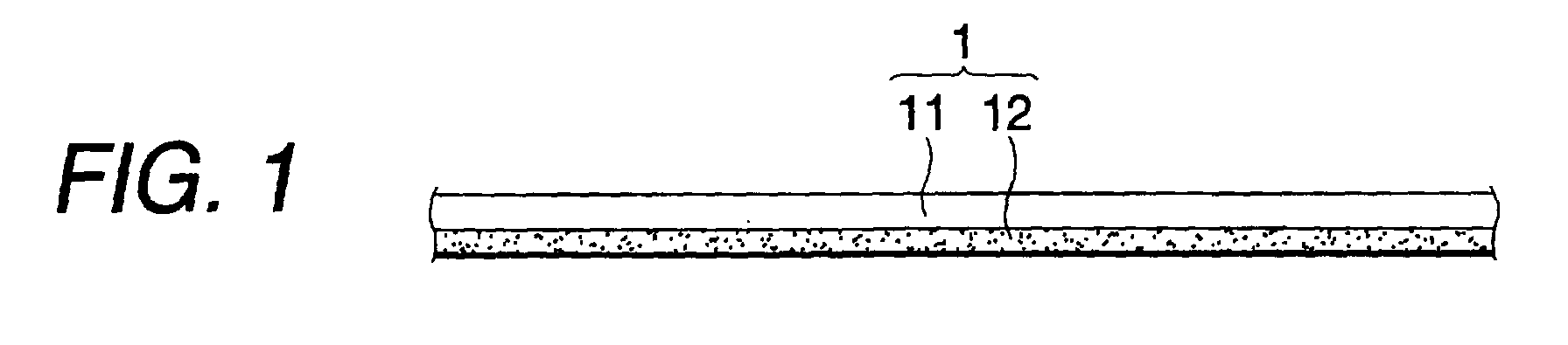
- Fig. 1 shows a release film 1 for semiconductor resin sealing according to the invention, which is comprising a base layer 11 and an auxiliary layer 12 having a lower compressive modulus than the base layer 11.
- Figs. 2A to 2D show an embodiment of the semiconductor resin sealing method according to the invention.
- the object to be sealed is semiconductor chips 2, of which the surface electrodes are bonded with wires 23 (see Fig. 2A) to inner terminals 22 of each unit 21 (see Fig. 3B) of a lead frame 2000 shown in Fig. 3A.
- Figs. 2A to 2D illustrate one unit 21 of the lead frame 2000.
- the semiconductor chip 2 is put in the cavity 31 of a heated cavity block (lower block) 3 of a transfer molding die with the inner terminals 22 up.
- the lower block 3 is closed by an upper block 4 via the release film 1 of Fig. 1 interposed therebetween with the auxiliary layer 12 facing down (see Fig. 28).
- a resin 5 is transferred into the cavity 31 and cured.
- the upper block 4 is lifted to open the molding die while the release film 1 is released from the cured resin 5 (see Fig. 2C).
- the lead frame 21 is then trimmed leaving the terminals 22 to obtain a QFN package.
- Fig. 2D is a cross section taken along line D-D in Fig. 2B. Having a low compressive modulus, the auxiliary layer 12 tightly fits in with an uneven surface thereby preventing the molten resin from penetrating into the contact interface with the terminals 22 and covering the terminals 22.
- the base layer 11 has a high compressive modulus, it has only a small compression strain and hardly flows laterally even under the mold clamping force.
- the auxiliary layer 12, which is likely to flow laterally, is blocked by the base layer 11 integral with the auxiliary layer 12 so that the thickness of the release film among the terminals 22 can be maintained substantially at the initial one. As a result, the space among the terminals can be filled with a sufficient amount of the resin, in which the terminals 22 are embedded firmly.
- the base layer 11 should be such as to be substantially prevented from compression deformation under the mold clamping force and at the mold temperature. Specifically, it is preferred for the base layer 11 to have a compressive modulus of 40 MPa or higher, more preferably 50 MPa or higher at 175°C.
- suitable base layers include plastic films of polyimide, aramid, polyether ketone, polyether sulfone, etc-and metal foils of copper, stainless steel, aluminum, etc.
- the thickness of the base layer 11 is not limited, but is preferably 500 ⁇ m or less, more preferably 5 to 50 ⁇ m, in view of handling, etc.
- the auxiliary layer 12 should be such as to have a low compressive modulus under the mold clamping force and at the mold temperature to assure excellent sealing properties for the terminals. Specifically, it is desirable for the auxiliary layer 12 to have a compressive modulus of less than 40 MPa, perferably 30 MPa or lower, particularly 20 MPa or lower, at 175°C.
- suitable auxiliary layers include fluororesins, such as polytetrafluoroethylene, tetrafluoroethylene-perfluoroalkyl vinyl ether copolymers, tetrafluoroethylene-hexafluoropropylene copolymers, polyvinylidene fluoride, and fluororubbers. The most suitable of them is polytetrafluoroethylene for its excellent release properties.
- the auxiliary layer made of a fluororubber can have formed thereon a thin fluororesin film of polytetrafluoroethylene, a tetrafluoroethylene-hexafluoropropylene copolymer, polyvinylidene fluoride, etc. to have improved release properties.
- the thickness of the auxiliary layer 12 should be as thin as is consistent with close fitting properties for the terminals. It is usually 5 to 50 ⁇ m, preferably 10 to 30 ⁇ m. A smaller thickness than 5 ⁇ m hardly assures fitting properties, and a larger thickness than 50 ⁇ m hardly secures a prescribed space to be filled with a resin among the terminals.
- the base layer and the auxiliary layer may be of a kind in material.
- the compressive modulus of the two layers can be adjusted appropriately by controlling at least one of molecular weight, crystallinity, porosity, orientation, and stretch properties.
- the composite film of the invention can be prepared usually by wet or dry lamination, coating, extrusion lamination, and the like.
- the resin sealing method of the invention is applied to semiconductor packages in which lead terminals are embedded while having the upper surface thereof exposed on the surface of the sealing resin. Therefore, the invention is applicable to not only the above-described QFN packages but other CSPs, such as those to be flip chip bonded having the terminals thereof to be brought into contact with external terminals (e.g., solder balls) exposed on the sealing resin surface, and packages by wafer level processing.
- a 50 ⁇ m thick polyimide (PI) film was used as a base layer.
- a 50% aqueous dispersion of tetrafluoroethylene powder was applied to the PI film, dried at 90°C for 2 minutes to evaporate water, and baked at 360°C for 2 minutes. The same operation was repeated once more to form a polytetrafluoroethylene (PTEF) auxiliary layer having a thickness of 25 ⁇ m.
- PTEF polytetrafluoroethylene
- release film had a total thickness of 75 ⁇ m.
- a release film having a total thickness of 75 ⁇ m was prepared in the same manner as in Example 1, except for using a 50 ⁇ m thick aluminum (Al) foil as a base layer.
- aqueous solution containing 50% of a fluororubber powder comprising a vinylidene fluoride unit in a major proportion and hexafluoropropylene unit in a minor proportion and 5% of a polyamine curing agent was applied to a 50 ⁇ m thick PI film as a base layer, dried at 90°C for 2 minutes to evaporate water, and baked at 300°C for 10 minutes. The same operation was repeated once more to form a fluororubber auxiliary layer having a thickness of 25 ⁇ m. The resulting release film had a total thickness of 75 ⁇ m.
- a release film comprising a 50 ⁇ m thick PI film as a base layer and a 7 ⁇ m thick fluororubber auxiliary layer was prepared in the same manner as in Example 3, except that the operation of applying the coating solution and baking was conducted only once.
- the resulting release film had a total thickness of 57 ⁇ m.
- a release film comprising a 50 ⁇ m thick PI film as a base layer and a 47 ⁇ m thick fluororubber auxiliary layer was prepared in the same manner as in Example 3, except that the operation of applying the coating solution and baking was conducted four times.
- the resulting release film had a total thickness of 97 ⁇ m.
- a release film comprising a 50 ⁇ m thick PI film as a base layer and a 25 ⁇ m thick fluororubber auxiliary layer was prepared in the same manner as in Example 3.
- a 20% aqueous dispersion of a tetrafluoroethylene-hexafluoropropylene copolymer (FEP) powder was applied to the fluororubber auxiliary layer of the release film, dried at 90°C for 2 minutes to remove water, and baked at 360°C for 2 minutes to form a thin FEP film having a thickness of 1 ⁇ m.
- the resulting release film had a total thickness of 76 ⁇ m.
- aqueous dispersion containing 50% of a tetrafluoroethylene powder was applied to a 100 ⁇ m thick PI sheet, dried at 90°C for 2 minutes to evaporate water, and baked at 360°C for 2 minutes. The same operation was repeated four times in all. The PI sheet was stripped off to obtain a 50 ⁇ m thick polytetrafluoroethylene (PTFE) film as a release film.
- PTFE polytetrafluoroethylene
- a 50 ⁇ m thick PI film was used as a release film.
- a 5 mm by 5 mm square was cut out of each of the release films prepared in Examples 1 to 6 and Comparative Examples 1 and 2.
- the auxiliary layer was peeled off the cut piece of Examples.
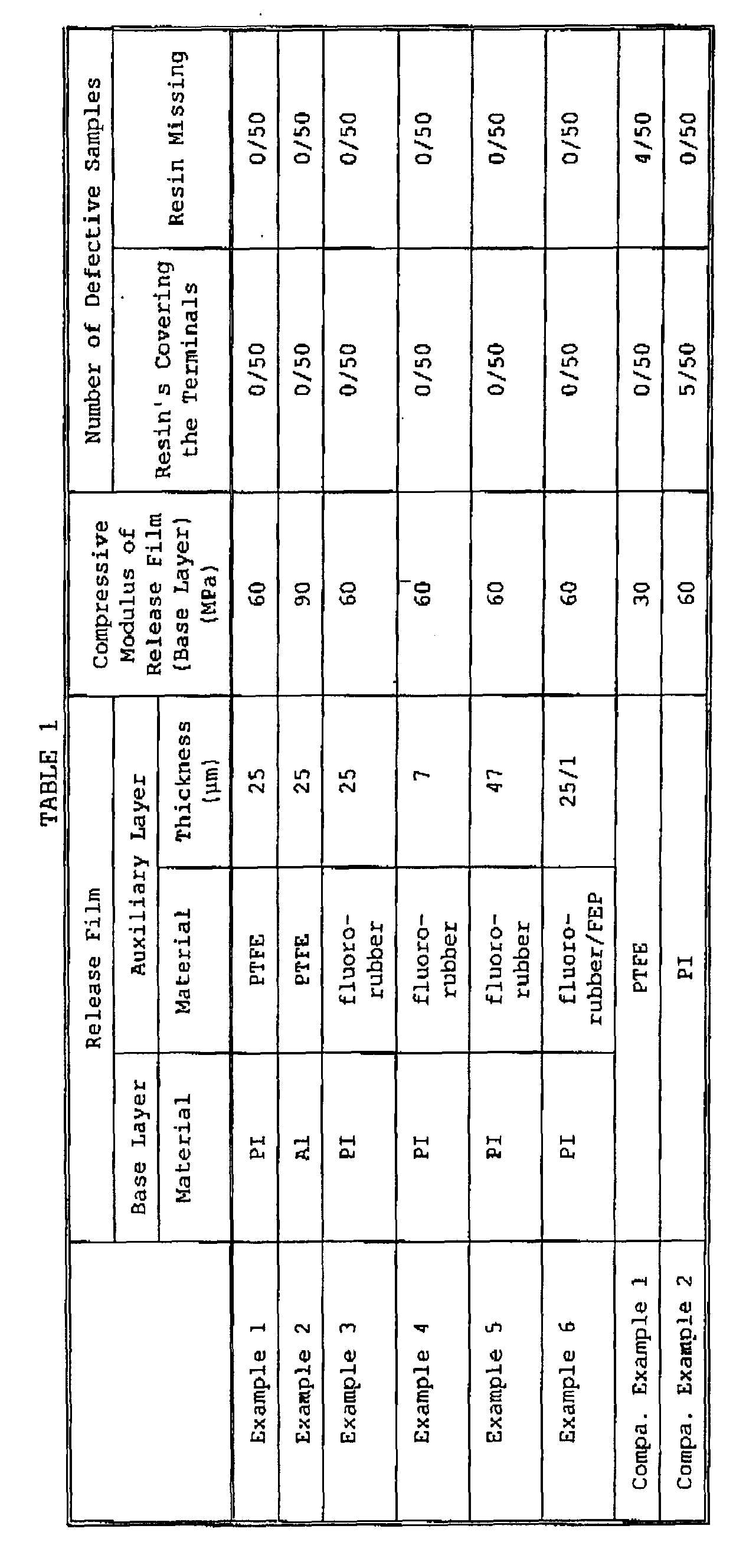
- the modulus in 10% compression of the test piece (a one layer release film or a base layer) was measured at 175°C with a viscoelasticity spectrometer by a penetration method under conditions of a needle diameter of 0.5 mm and a loading rate of 50 gf/min. The results obtained are shown in Table 1 below.
- the release film of Comparative Example 1 fails to completely avoid resin missing between the terminals, which is the result of resin starvation between the terminals due to the downward protrusion of the release film between the terminals because of the low compressive modulus of the release film.
- the release film fails to completely get rid of the resin's covering the terminals. This is the result of the release film failing to fit the terminals because of its high compressive modulus.
- both resin missing and resin's covering the terminals can be prevented in the present invention by combining a base layer having a high compressive modulus and an auxiliary layer having a low compressive modulus. It was confirmed that the release film of Example 6 exhibits particularly excellent release properties owing to the tetrafluoroethylene-hexafluoropropylene copolymer thin film provided on its surface, achieving smooth release of packages by their own weight.
- the chips in packaging semiconductor chips while leaving the upper surface of the terminals or electrodes exposed by resin sealing using a release film, the chips can be sealed in a resin in high yield without suffering from resin's covering the terminals or electrodes or resin missing among the terminals which have been often observed with release films of the related art.
- This effect leads to reduction or elimination of a release agent from a sealing resin, which will bring about improvement in sealing performance of the sealing resin and further reduction of package size. Therefore, the invention gives an advantage to the chip size packaging technology. Additionally, the invention makes it possible to reduce the mold cleaning frequency, which will lead to improved working efficiency and an extended life of the mold (i.e., cost reduction), and also to omit ejection pins, which means simplification of the mold structure.
Landscapes
- Engineering & Computer Science (AREA)
- Mechanical Engineering (AREA)
- Encapsulation Of And Coatings For Semiconductor Or Solid State Devices (AREA)
- Moulds For Moulding Plastics Or The Like (AREA)
- Injection Moulding Of Plastics Or The Like (AREA)
- Laminated Bodies (AREA)
Abstract
Description
Claims (8)
- A resin sealing method for semiconductors, which comprises molding a resin with a release film interposed between a molding die and a sealing surface of a semiconductor chip having terminals or electrodes in such a manner that the sealed semiconductor chip may have the tips of said terminals or electrodes exposed on the surface of the cured resin which has been in contact with the release film, wherein said release film is a composite film comprising a base layer and an auxiliary layer having a lower compressive modulus than the base layer, and the release film is used with said auxiliary layer facing the sealing surface of the semiconductor chip.
- A release film used in resin sealing of semiconductor chips which is a composite film comprising a base layer and an auxiliary layer having a lower compressive modulus than the base layer, and the release film is used with said auxiliary layer facing the sealing surface of semiconductor chips.
- The release film according to claim 2, wherein said base layer has a compressive modulus of 50 MPa or more at 175°C.
- The release film according to claim 2, wherein said auxiliary layer comprises a fluororesin.
- The release film according to claim 2, wherein said auxiliary layer comprises a fluororubber.
- The release film according to claim 2, wherein said auxiliary layer has a thin fluororesin film on the surface thereof.
- The release film according to claim 2, wherein said auxiliary layer has a compressive modulus of 30 Mpa or less at 175°C.
- The release film according to claim 2, wherein said auxiliary layer has a thickness of 5 to 50 µm.
Applications Claiming Priority (4)
| Application Number | Priority Date | Filing Date | Title |
|---|---|---|---|
| JP36959399 | 1999-12-27 | ||
| JP36959399 | 1999-12-27 | ||
| JP2000090039 | 2000-03-29 | ||
| JP2000090039A JP4443715B2 (en) | 1999-12-27 | 2000-03-29 | Semiconductor resin sealing method and semiconductor resin sealing release film |
Publications (2)
| Publication Number | Publication Date |
|---|---|
| EP1113490A2 true EP1113490A2 (en) | 2001-07-04 |
| EP1113490A3 EP1113490A3 (en) | 2004-01-02 |
Family
ID=26582128
Family Applications (1)
| Application Number | Title | Priority Date | Filing Date |
|---|---|---|---|
| EP20000128590 Withdrawn EP1113490A3 (en) | 1999-12-27 | 2000-12-27 | Resin sealing method for semiconductors and release film used therefor |
Country Status (5)
| Country | Link |
|---|---|
| US (2) | US20020142153A1 (en) |
| EP (1) | EP1113490A3 (en) |
| JP (1) | JP4443715B2 (en) |
| KR (1) | KR20010062784A (en) |
| TW (1) | TW530355B (en) |
Cited By (2)
| Publication number | Priority date | Publication date | Assignee | Title |
|---|---|---|---|---|
| EP1333480A3 (en) * | 2002-01-31 | 2004-08-25 | STMicroelectronics, Inc. | Transfer molding process for an integrated circuit and pre-formed release film for use in this process |
| EP1612021A1 (en) * | 2004-06-29 | 2006-01-04 | Asahi Glass Company Ltd. | Release film for encapsulation of semiconductor chip |
Families Citing this family (10)
| Publication number | Priority date | Publication date | Assignee | Title |
|---|---|---|---|---|
| US20050242425A1 (en) * | 2004-04-30 | 2005-11-03 | Leal George R | Semiconductor device with a protected active die region and method therefor |
| JP2006049850A (en) * | 2004-06-29 | 2006-02-16 | Asahi Glass Co Ltd | Release film for semiconductor chip sealing |
| JP4654062B2 (en) * | 2005-03-30 | 2011-03-16 | 株式会社巴川製紙所 | Adhesive sheet for manufacturing semiconductor device and method for manufacturing semiconductor device |
| KR20090018032A (en) | 2006-04-25 | 2009-02-19 | 아사히 가라스 가부시키가이샤 | Release film for semiconductor resin mold |
| KR102444374B1 (en) | 2015-02-06 | 2022-09-16 | 에이지씨 가부시키가이샤 | Film, method for producing same, and method for producing semiconductor element using film |
| NL2021058B1 (en) * | 2018-06-05 | 2019-12-11 | Besi Netherlands Bv | Method, foil, mould part and surface layer for encapsulating electronic components mounted on a carrier using expansion spaces absorbing local foil layer displacements |
| WO2020071388A1 (en) * | 2018-10-04 | 2020-04-09 | 日東電工株式会社 | Heat-resistant release sheet and thermocompression bonding method |
| JP7240339B2 (en) * | 2020-01-20 | 2023-03-15 | Towa株式会社 | Method for manufacturing resin molded product and resin molding apparatus |
| CN117480043B (en) | 2021-08-25 | 2026-06-30 | 电化株式会社 | Thermoplastic release film for semiconductor packaging process and method for manufacturing electronic component using same |
| JP7239791B1 (en) | 2021-08-25 | 2023-03-14 | デンカ株式会社 | Thermoplastic release film for semiconductor encapsulation process and method for manufacturing electronic components using the same |
Family Cites Families (6)
| Publication number | Priority date | Publication date | Assignee | Title |
|---|---|---|---|---|
| US5674343A (en) * | 1994-04-19 | 1997-10-07 | Nitto Denko Corporation | Method for manufacturing a semiconductor |
| US5949132A (en) * | 1995-05-02 | 1999-09-07 | Texas Instruments Incorporated | Dambarless leadframe for molded component encapsulation |
| JP3129660B2 (en) * | 1996-07-23 | 2001-01-31 | アピックヤマダ株式会社 | Resin sealing method and resin sealing device for SON package |
| US6048483A (en) * | 1996-07-23 | 2000-04-11 | Apic Yamada Corporation | Resin sealing method for chip-size packages |
| KR100214555B1 (en) * | 1997-02-14 | 1999-08-02 | 구본준 | Manufacturing method of semiconductor package |
| JP3017470B2 (en) * | 1997-07-11 | 2000-03-06 | アピックヤマダ株式会社 | Resin molding method and resin molding device |
-
2000
- 2000-03-29 JP JP2000090039A patent/JP4443715B2/en not_active Expired - Lifetime
- 2000-12-27 US US09/748,199 patent/US20020142153A1/en not_active Abandoned
- 2000-12-27 EP EP20000128590 patent/EP1113490A3/en not_active Withdrawn
- 2000-12-27 KR KR1020000083277A patent/KR20010062784A/en not_active Withdrawn
- 2000-12-27 TW TW89128008A patent/TW530355B/en not_active IP Right Cessation
-
2002
- 2002-11-27 US US10/304,944 patent/US20030087088A1/en not_active Abandoned
Cited By (3)
| Publication number | Priority date | Publication date | Assignee | Title |
|---|---|---|---|---|
| EP1333480A3 (en) * | 2002-01-31 | 2004-08-25 | STMicroelectronics, Inc. | Transfer molding process for an integrated circuit and pre-formed release film for use in this process |
| US7595017B2 (en) | 2002-01-31 | 2009-09-29 | Stmicroelectronics, Inc. | Method for using a pre-formed film in a transfer molding process for an integrated circuit |
| EP1612021A1 (en) * | 2004-06-29 | 2006-01-04 | Asahi Glass Company Ltd. | Release film for encapsulation of semiconductor chip |
Also Published As
| Publication number | Publication date |
|---|---|
| EP1113490A3 (en) | 2004-01-02 |
| US20030087088A1 (en) | 2003-05-08 |
| KR20010062784A (en) | 2001-07-07 |
| JP2001250838A (en) | 2001-09-14 |
| US20020142153A1 (en) | 2002-10-03 |
| TW530355B (en) | 2003-05-01 |
| JP4443715B2 (en) | 2010-03-31 |
Similar Documents
| Publication | Publication Date | Title |
|---|---|---|
| US20020142153A1 (en) | Resin sealing method for semiconductors and release film used therefor | |
| TWI707758B (en) | Release film, its manufacturing method, and semiconductor package manufacturing method | |
| TWI505416B (en) | Adhesive tape for resin sealing and manufacturing method of resin-sealed type semiconductor device using the same | |
| JP2006049850A (en) | Release film for semiconductor chip sealing | |
| JP2004296555A (en) | Semiconductor device manufacturing method and semiconductor device | |
| US20130337614A1 (en) | Methods for manufacturing a chip package, a method for manufacturing a wafer level package, and a compression apparatus | |
| TW201232674A (en) | Method and apparatus of compression molding for reducing viods in molding compound | |
| JP4619486B2 (en) | Lead frame laminate and method for manufacturing semiconductor component | |
| JP3578262B2 (en) | Resin sealing method for semiconductor chip and release film used in the method | |
| EP1612021B1 (en) | Release film for encapsulation of semiconductor chip | |
| JP3207286B2 (en) | Resin-sealed semiconductor device | |
| TW202012140A (en) | Release film for semiconductor packaging process and manufacturing method of electronic parts using the same | |
| KR101168861B1 (en) | Semiconductor device and method of manufacturing thereof | |
| JP2000195883A (en) | Resin sealing method for semiconductor wafer | |
| JP4454774B2 (en) | Semiconductor chip resin sealing method and release film for semiconductor chip resin sealing | |
| JP2000299333A (en) | Semiconductor device manufacturing method | |
| TWI295091B (en) | Coating for enhancing adhesion of molding compound to semiconductor devices | |
| EP2636712A1 (en) | Pressure-sensitive adhesive tape for resin encapsulation and method for producing resin encapsulation type semiconductor device | |
| KR101923736B1 (en) | Pressure-sensitive adhesive tape for resin encapsulation and method for producing resin encapsulation type semiconductor device | |
| JP2000141400A (en) | Resin sealing method for semiconductor device | |
| TWI701783B (en) | Semiconductor device | |
| TWI528467B (en) | Pressure-sensitive adhesive tape for resin encapsulation and method for manufacturing resin-encapsulated semiconductor device | |
| JP2002222911A (en) | Lead frame laminate and method of manufacturing semiconductor device | |
| HK1073178B (en) | Adhesive sheet for semiconductor device production, semiconductor device using the same, and production method of semiconductor device | |
| HK1073178A1 (en) | Adhesive sheet for semiconductor device production, semiconductor device using the same, and production method of semiconductor device |
Legal Events
| Date | Code | Title | Description |
|---|---|---|---|
| PUAI | Public reference made under article 153(3) epc to a published international application that has entered the european phase |
Free format text: ORIGINAL CODE: 0009012 |
|
| AK | Designated contracting states |
Kind code of ref document: A2 Designated state(s): AT BE CH CY DE DK ES FI FR GB GR IE IT LI LU MC NL PT SE TR |
|
| AX | Request for extension of the european patent |
Free format text: AL;LT;LV;MK;RO;SI |
|
| PUAL | Search report despatched |
Free format text: ORIGINAL CODE: 0009013 |
|
| AK | Designated contracting states |
Kind code of ref document: A3 Designated state(s): AT BE CH CY DE DK ES FI FR GB GR IE IT LI LU MC NL PT SE TR |
|
| AX | Request for extension of the european patent |
Extension state: AL LT LV MK RO SI |
|
| 17P | Request for examination filed |
Effective date: 20040415 |
|
| AKX | Designation fees paid |
Designated state(s): AT BE CH CY DE DK ES FI FR GB GR IE IT LI LU MC NL PT SE TR |
|
| STAA | Information on the status of an ep patent application or granted ep patent |
Free format text: STATUS: THE APPLICATION IS DEEMED TO BE WITHDRAWN |
|
| 18D | Application deemed to be withdrawn |
Effective date: 20060701 |