EP1111522A2 - Computer-aided design supporting system in which cells can be arranged independently - Google Patents
Computer-aided design supporting system in which cells can be arranged independently Download PDFInfo
- Publication number
- EP1111522A2 EP1111522A2 EP00128107A EP00128107A EP1111522A2 EP 1111522 A2 EP1111522 A2 EP 1111522A2 EP 00128107 A EP00128107 A EP 00128107A EP 00128107 A EP00128107 A EP 00128107A EP 1111522 A2 EP1111522 A2 EP 1111522A2
- Authority
- EP
- European Patent Office
- Prior art keywords
- cell
- pattern
- patterns
- power supply
- ground
- Prior art date
- Legal status (The legal status is an assumption and is not a legal conclusion. Google has not performed a legal analysis and makes no representation as to the accuracy of the status listed.)
- Withdrawn
Links
Images




Classifications
-
- H—ELECTRICITY
- H10—SEMICONDUCTOR DEVICES; ELECTRIC SOLID-STATE DEVICES NOT OTHERWISE PROVIDED FOR
- H10D—INORGANIC ELECTRIC SEMICONDUCTOR DEVICES
- H10D84/00—Integrated devices formed in or on semiconductor substrates that comprise only semiconducting layers, e.g. on Si wafers or on GaAs-on-Si wafers
- H10D84/90—Masterslice integrated circuits
- H10D84/903—Masterslice integrated circuits comprising field effect technology
- H10D84/907—CMOS gate arrays
-
- G—PHYSICS
- G06—COMPUTING OR CALCULATING; COUNTING
- G06F—ELECTRIC DIGITAL DATA PROCESSING
- G06F30/00—Computer-aided design [CAD]
- G06F30/30—Circuit design
- G06F30/39—Circuit design at the physical level
Definitions
- the present invention relates to a computer-aided design supporting system for arranging cells independently with reference to a cell library.
- a computer-aided design supporting system is often used to automatically arrange and connect function blocks or "cells".
- Such a computer-aided design supporting system is disclosed in, for example, Japanese Laid Open Patent Application (JP-A-Heisei 6-85062).
- the computer-aided design supporting system has a cell library, which stores patterns of circuits such as basic gates and logic circuits, which have a high use frequency as standard cells.
- the standard cell is composed of a logic circuit section, a power supply section and a ground section.
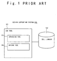
- Fig. 1 shows the structure of the conventional computer-aided design supporting system 100.
- the design supporting system 100 is composed of a CAD tool 101 and a cell library 102.
- the CAD tool 101 is composed of an arranging tool 103 and a wiring tool 104.
- the CAD tool 101 is carries out automatic arrangement and connection of the cells.
- the cell library 102 is a database in which various standard cells are registered.
- the arranging tool 103 reads out the standard cells from the cell library 102 and automatically arranges the read out standard cells on a cell track provided in an arrangement region.
- the wiring tool 104 automatically connects between the standard cells on the cell track and between the standard cells and wiring lines on a wiring tack in the arrangement region.
- Fig. 2 shows the structure of a conventional standard cell 110.
- the standard cell 110 is composed of a power supply section 111, a logic circuit section 112, and a ground section 113.
- the standard cell 110 is arranged on the cell track, using the power supply section 111, the logic circuit section 112 and the ground section 113 as a unit.
- Figs. 3A to 3C show the arrangement of the conventional standard cells.
- Fig. 3A shows the state in which three standard cells 110a are arranged on a cell track T10, and three standard cells 110b are arranged on a cell track T11.
- the ground sections 113b of the standard cells 110b overlap the ground terminal sections 113a of the standard cells 110a.
- the ground sections 113b of the standard cells 110b are arranged on the cell track T10.
- the arrangement region will be used more effectively. If a wiring track should be arranged between the cell tracks, the power supply sections or the ground sections are independently arranged. In this case, however, the arrangement region cannot be utilized effectively.
- the height of the power supply section or ground section namely, the dimension in the direction in which the power supply section and the ground section are aligned in the standard cell, can be selected optionally.
- the amount of current that flows in the standard cell can be selected optionally.
- the standard cells are different power supply sections and different ground sections in height and permissible current value. For this reason, a great number of standard cells need to be registered in the cell library, so that a selecting operation of standard cells is complicated in case of arrangement of the standard cell.
- an object of the present invention is to provide a computer-aided design supporting system in which power supply cell patterns, logic cell patterns and ground cell patterns can be arranged individually and independently.
- Another object of the present invention is to provide a computer-aided design supporting system in which an arranged power supply cell pattern, an arranged logic cell pattern and an arranged ground cell pattern are automatically connected to each other.
- Still another object of the present invention is to provide a computer-aided design supporting system in which an arranged power supply cell pattern, an arranged logic cell pattern and an arranged ground cell pattern constitutes a pattern of a logic device as a unit.
- Yet still another object of the present invention is to provide a computer-aided design supporting system in which an arranged power supply cell pattern, an arranged logic cell pattern and an arranged ground cell pattern can be changed or moved as a unit.
- a computer-aided design supporting system for a semiconductor device includes a cell library, an arranging tool and a wiring tool.
- the cell library stores a plurality of logic cell patterns, a plurality of power supply cell patterns, and a plurality of ground cell patterns.
- a logic device pattern of the semiconductor device includes one of the plurality of logic cell patterns, one of the plurality of power supply cell patterns, and one of the plurality of ground cell patterns.
- the arranging tool arranges selected ones of the plurality of logic cell patterns, selected ones of the plurality of power supply cell patterns and selected ones of the plurality of ground cell patterns on cell tracks individually and independently in response to an arrange instruction.
- the wiring tool connects between the selected logic cell patterns, between the selected power supply cell patterns and between the selected ground cell patterns arranged on the cell tracks in response to a wiring instruction to form a pattern of the semiconductor. device.
- a pattern of a specific logic device may include a specific one of the selected logic cell patterns, a specific one of the selected power supply cell patterns and a specific one of the selected ground cell patterns. Also, it is supposed that after one of the specific logic cell pattern, a specific power supply cell pattern and a specific ground cell pattern is arranged by the arranging tool, another may be arranged by the arranging tool with respect to the one cell pattern. In this case, the one cell pattern and the other cell pattern are automatically connected.
- the plurality of power supply cell patterns are grouped in a plurality of groups, and the plurality of ground cell patterns are grouped in a plurality of groups.
- the plurality of groups for the plurality of power supply cell patterns may be different from each other in at least one of a height of cell pattern, the number of power supply lines, and a permissible current value.
- the plurality of groups for the plurality of ground cell patterns may be different from each other in at least one of a height of cell pattern, the number of ground lines, and a permissible current value.
- the arranging tool may include a logic cell tool, a power supply cell tool and a ground cell-tool.
- the logic cell tool arranges each of the selected logic cell patterns on either of the cell tracks in response to a logic cell arrangement instruction.
- the power supply cell tool arranges each of the selected power supply cell patterns on either of the cell tracks in response to a power supply cell arrangement instruction.
- the ground cell tool arranges each of the selected ground cell patterns on either of the cell tracks in response to a ground cell arrangement instruction.
- a specified logic device may include a specified one of the selected logic cell patterns, a specified one of the selected power supply cell patterns and a specific one of the selected ground cell patterns.
- the arranging tool transforms the specified logic device pattern in response to a move instruction while maintaining connections between the cell patterns such that the specified logic cell pattern and one of the specific power supply cell pattern and the specific ground cell pattern are automatically moved as a unit.
- the logic cell tool moves the specified logic cell pattern in response to the move instruction.
- the power cell tool moves the specified power supply cell pattern in response to the move instruction, and the ground cell tool maintaining connection between the specified logic cell pattern and the specified ground cell pattern.
- the logic cell tool moves the specified logic cell pattern in response to the move instruction.
- the ground tool moves the specified ground cell pattern in response to the move instruction, and the power supply cell tool maintaining connection between the specified logic cell pattern and the specified power supply cell pattern.
- a computer-aided design supporting method for a semiconductor device is attained by providing a cell library which stores a plurality of logic cell patterns, a plurality of power supply cell patterns, and a plurality of ground cell patterns, wherein a logic device pattern of the semiconductor device includes one of the plurality of logic cell patterns, one of the plurality of power supply cell patterns, and one of the plurality of ground cell patterns; by arranging selected ones of the plurality of logic cell patterns, selected ones of the plurality of power supply cell patterns and selected ones of the plurality of ground cell patterns on cell tracks individually and independently in response to an arrange instruction; and by connecting between the selected logic cell patterns, between the selected power supply cell patterns and between the selected ground cell patterns arranged on the cell tracks in response to a wiring instruction to form a pattern of the semiconductor device.
- a pattern of a specific logic device may include a specific one of the selected logic cell patterns, a specific one of the selected power supply cell patterns and a specific one of the selected ground cell patterns. Also, after one of the specific logic cell pattern, a specific power supply cell pattern and a specific ground cell pattern is arranged by the arranging tool, another may be arranged by the arranging tool with respect to the one cell pattern. In this case, the arrangement is attained by automatically connecting the one cell pattern and the other cell pattern.
- the plurality of power supply cell patterns may be grouped in a plurality of groups, and the plurality of ground cell patterns may be grouped in a plurality of groups.
- the plurality of groups for the plurality of power supply cell patterns are different from each other in at least one of a height of cell pattern, the number of power supply lines, and a permissible current value.
- the plurality of groups for the plurality of ground cell patterns are different from each other in at least one of a height of cell pattern, the number of ground lines, and a permissible current value.
- the arrangement may be attained by arranging each of the selected logic cell patterns on either of the cell tracks by a logic cell tool in response to a logic cell arrangement instruction; by arranging each of the selected power supply cell patterns on either of the cell tracks by a power supply cell tool in response to a power supply cell arrangement instruction; and by arranging each of the selected ground cell patterns on either of the cell tracks by a ground cell tool in response to a ground cell arrangement instruction.
- the method may further includes a method attained by transforming the specified logic device pattern in response to a move instruction while maintaining connections between the cell patterns such that the specified logic cell pattern and one of the specific power supply cell pattern and the specific. ground cell pattern are automatically moved as a unit.
- the transformation may be attained by moving the specified logic cell pattern in response to the move instruction.
- the transformation may be attained by moving the specified power supply cell pattern in response to the move instruction, and by maintaining connection between the specified logic cell pattern and the specified ground cell pattern.
- the transformation may be attained by moving the specified logic cell pattern in response to the move instruction.
- the transformation may be attained by moving the specified ground cell pattern in response to the move instruction, and maintaining connection between the specified logic cell pattern and the specified power supply cell pattern.
- a recording medium which stores a cell library having a plurality of logic cell patterns, a plurality of power supply cell patterns, and a plurality of ground cell patterns.
- a logic device pattern of the semiconductor device includes one of the plurality of logic cell patterns. one of the plurality of power supply cell patterns, and one of the plurality of ground cell patterns.
- the recording medium also stores a program stores for a method which is attained by arranging selected ones of the plurality of logic cell patterns, selected ones of the plurality of power supply cell patterns and selected ones of the plurality of ground cell patterns on cell tracks individually and independently in response to an arrange instruction; and by connecting between the selected logic cell patterns, between the selected power supply cell patterns and between the selected ground cell patterns arranged on the cell tracks in response to a wiring instruction to form a pattern of the semiconductor device.
- a pattern of a specific logic device may include a specific one of the selected logic cell patterns, a specific one of the selected power supply cell patterns and a specific one of the selected ground cell patterns, and after one of the specific logic cell pattern, a specific power supply cell pattern and a specific ground cell pattern is arranged by the arranging tool, another may be arranged by the arranging tool with respect to the one cell pattern. In this case, the arrangement may be attained by automatically connecting the one cell pattern and the other cell pattern.
- the arrangement may be attained by arranging each of the selected logic cell patterns on either of the cell tracks by a logic cell tool in response to a logic cell arrangement instruction; by arranging each of the selected power supply cell patterns on either of the cell tracks by a power supply cell tool in response to a power supply cell arrangement instruction; and by arranging each of the selected ground cell patterns on either of the cell tracks by a ground cell tool in response to a ground cell arrangement instruction.
- the method may further include transforming the specified logic device pattern in response to a move instruction while maintaining connections between the cell patterns such that the specified logic cell pattern and one of the specific power supply cell pattern and the specific ground cell pattern are automatically moved as a unit.
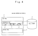
- Fig. 1 shows the structure of a computer-aided design supporting system 1 according to an embodiment of the present invention.
- the computer-aided design supporting system 1 is composed of a CAD tool 2 and a cell library 3.
- the CAD tool 2 is composed of an arranging tool 4 and a wiring tool 5.
- the arranging tool 4 has a logic cell tool 6, a power-supply cell tool 7 and a ground cell tool 8.
- the cell library 3 stores a plurality of types of standard logic cell patterns, a plurality of types of standard power supply cell patterns and a plurality of types of ground cell patterns.
- the plurality of types of standard power supply cell patterns are different from each other in height, the number of power supply lines or permissible current value.
- the plurality of types of ground cell patterns are different from each other in height, the number of ground lines or permissible current value.
- a pattern of a logic device is composed of a set of a power supply cell pattern, a logic cell pattern and a ground cell pattern.
- the CAD tool 2 is a processor that carries out the automatic arrangement and connection of cell patterns.
- the arranging tool 4 reads out the standard cell pattern from the cell library 3 in response to an arrange instruction individually and independently.
- the arranging tool 4 automatically arranges the read out standard cell pattern on a cell track provided in an arrangement region.
- the wiring tool 5 automatically connects between the standard cell patterns for different logic device patterns on the cell track, and between the standard cell patterns and wiring lines on the wiring track in the arrangement region.
- the logic cell tool 6 arranges a standard logic cell pattern in response to a logic cell arrange instruction of the arrange instruction.
- the power supply cell tool 7 arranges a standard power supply cell pattern in response to a power supply cell arrange instruction of the arrange instruction.
- the ground cell tool 8 arranges a standard ground cell pattern in response to a ground cell arrange instruction of the arrange instruction.
- Figs. 5B to 5E are show the structure of the standard cell pattern according the present invention.
- the cell library 3 has the first standard power supply cell pattern 70a and the second standard power supply cell pattern 70b as the standard cell patterns.
- the cell library 3 further has a standard logic cell pattern 60 as the standard cell pattern.
- the cell library 3 has the first standard ground cell pattern 80a and the second standard ground cell pattern 80b as the standard cell patterns.
- the first standard power supply cell pattern 70a and the first standard ground cell pattern 80a are small current cell patterns.
- the second standard power supply cell pattern 70b and the second standard ground cell pattern 80b are large current cell patterns.
- the standard logic cell pattern 60 is arranged on a cell track by the logic cell tool 6 in response to the logic cell arrange instruction.
- the standard power supply cell patterns 71 to 75 are arranged above the standard logic cell pattern 60 by the power supply cell tool 7 and the standard ground cell patterns 81 to 85 are arranged under the standard logic cell pattern 60 by the ground cell tool 8.
- a wiring line pattern of the power supply cell pattern 75 is connected to a wiring line pattern of the standard logic cell pattern 60 by the power supply cell tool 7.
- the standard ground cell 85 when the standard ground cell 85 is arranged adjacently to the standard logic cell pattern 60 on the cell track in response to the ground cell arranging instruction, a wiring line pattern of the ground cell pattern 85 is connected to a wiring line pattern of the standard logic cell pattern 60 by the ground cell tool 7.
- the standard power supply cell 75, the standard logic cell pattern 60 and the standard ground cell 85 are made unitary as a pattern of a logic device.
- the standard logic cell pattern 60 has neither a power supply cell pattern nor a ground cell pattern.
- the standard logic cell pattern 60 is used in combination with the standard power supply cell pattern and the standard ground cell pattern.
- Fig. 6A shows an arrangement of the standard cell patterns according to the embodiment of the present invention.
- Fig. 6B shows a rearrangement of the standard cell patterns in which a wiring track is newly provided between two adjacent cell tracks.
- a logic cell pattern group 600 composed of three standard logic cell patterns
- a power supply cell pattern group 700 composed of three standard power supply cell patterns
- a ground cell pattern group 800 composed of six ground cell patterns on a cell track T20.
- a logic cell pattern group 601 composed of three standard logic ells
- a power supply cell pattern group 701 composed of three standard power supply cell patterns on a cell track T21.
- the first three are connected to the three standard logic cell patterns of the logic cell pattern group 600, respectively. Also, the remaining three are connected to the three standard logic cell patterns of the logic cell pattern group 601, respectively. The remaining three standard ground cell patterns are arranged to overlap the first three standard ground cell patterns.
- the power supply cell tool 7 controls the arrangement of the standard power supply cell patterns.
- the logic cell tool 6 controls the arrangement of the standard logic cell patterns
- the ground cell tool 8 controls the arrangement of the standard ground cell patterns.
- the power supply cell pattern group 701 is moved by the power supply cell tool 7 in response to a change (move) instruction.
- the arranging tool 4 temporarily stored a movement quantity of the power supply cell group 701.
- the logic cell tool 6 is automatically initiated after the operation of the power supply cell tool 7.
- the logic cell pattern group 601 is moved by the movement quantity by the logic cell tool 6.
- wiring line patterns extend from the standard ground cell patterns to the standard logic cell patterns.
- the ground cell tool 8 maintains the respective connections between the ground cell pattern group 800 and the logic cell pattern group 601.
- the wiring track T22 is formed by moving the power supply cell pattern group 701 and logic cell pattern group 601, as shown in Fig. 6B.
- the wiring tool 5 is initiated so that the ground cell patterns are connected to wiring lines of the wiring track T22.
- Fig. 6C shows the arrangement of the standard cell patterns according to the embodiment of the present invention. This figure is similar to Fig. 6A.
- Fig. 6D shows an arrangement of the standard cell patterns in which the standard ground cell patterns of the ground cell pattern group are changed in height.
- a logic cell pattern group 600 composed of three standard logic cell patterns
- a power supply cell pattern group 700 composed of three standard power supply cell patterns
- a ground cell pattern group 800 composed of six ground cell patterns on a cell track T20.
- a logic cell pattern group 601 composed of three standard logic ells
- a power supply cell pattern group 701 composed of three standard power supply cell patterns on a cell track T21.
- the first three are connected to the three standard logic cell patterns of the logic cell pattern group 600, respectively. Also, the remaining three are connected to the three standard logic cell patterns of the logic cell pattern group 601, respectively. The remaining three standard ground cell patterns are arranged to overlap the first three standard ground cell patterns.
- the power supply cell tool 7 controls the arrangement of the standard power supply cell patterns.
- the logic cell tool 6 controls the arrangement of the standard logic cell patterns
- the ground cell tool 8 controls the arrangement of the standard ground cell patterns.
- the ground cell tool 8 receives a change instruction to change the ground cell patterns of the group 800 in height. At this time, the ground cell tool 8 carries out a changing process of all the ground cell patterns of the group 800 at a time. For example, when the cell patterns of the ground cell pattern group 800 are changed to the second standard cell patterns 80b, the ground cell tool 8 reads the second standard ground cell patterns 80b from the cell library 3 in response to a change (substitute) instruction. Then, the tool 8 arranges the second standard ground cell patterns 80b in the ground cell pattern group 800 in place of the first standard ground cell patterns 80a, as shown in Fig. 6D. In this case, prior to the ground cell tool 8, the power supply cell tool 7 and the logic cell tool 6 are started.
- the power supply cell pattern group 701 is moved by the power supply cell tool 7 in response to a change (move) instruction.
- the arranging tool 4 temporarily stored a movement quantity of the power supply cell group 701.
- the logic cell tool 6 is automatically initiated after the operation of the power supply cell tool 7.
- the ground cell tool 8 is started to substitute the second standard ground cell patterns 80b for the first standard ground cell patterns 80a, as shown in Fog. 6D.
- wiring line patterns of the standard ground cell patterns of the group 801 are connected to the wiring line patterns of the standard logic cell patterns of the group 601
- the wiring tool 5 is initiated so that the standard ground cell patterns are connected to wiring lines of the wiring track T22.
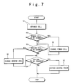
- Fig. 7 is a flowchart showing the operation of the arranging tool 4 of the present invention.
- the logic cell tool 6 of the tool 4 Upon receipt of a cell pattern arranging instruction, the logic cell tool 6 of the tool 4 reads the standard logic cell pattern 60 from the cell library 3 to arrange on a predetermined cell track.
- the power supply cell tool 7 reads the standard power supply cell patterns 70a and 70b from the cell library 3 to arrange on the predetermined cell track.
- the ground cell tool 8 reads the standard ground cell patterns 80a and 80b from the cell library 3 to arrange on the predetermined cell track (Step S1).
- the power supply cell tool 7 monitors an instruction for changing the standard power supply cell patterns (Step S2).
- To change the standard power supply cell patterns is to change the cell pattern 70a to the cell pattern 70b, and the cell pattern 70b to the cell pattern 70a.
- the ground cell tool 8 keeps monitoring an instruction for changing the standard ground cell patterns (Step S3).
- To change the standard ground cell patterns is to change the cell pattern 80a to the cell pattern 80b, and the cell pattern 80b to the cell pattern 80a.
- the logic cell tool 6 keeps monitoring an instruction for moving the cell track (Step S3). The cell track is moved when it is necessary to provide a new wiring track, to expand the existing wiring track or to compress the same.
- the arranging tool 4 keeps waiting for a new instruction.
- the power supply cell tool 7 Upon detecting an instruction for changing the standard power supply cell patterns, the power supply cell tool 7 reads a new standard power supply cell pattern from the cell library 3. The power supply cell tool 7 arranges the new standard power supply cell pattern on a predetermined power supply cell pattern group, as described above (Step S5).
- the ground cell tool 8 Upon detecting an instruction for changing the standard ground cell patterns, the ground cell tool 8 reads a new standard ground cell pattern from the cell library 3. The tool 8 arranges a new standard ground cell pattern on a predetermined ground cell pattern group, as described above (Step S6).
- the logic cell tool 6, the power supply cell tool 7 and the ground cell tool 8 rearrange the standard logic cell patterns, the standard power supply cell patterns and the standard ground cell patterns on a new cell track (Step S7).
- the grounding position can be located far from the grounding position to the substrate with respect to the logic cell pattern. Hence, the effect of measures to noise at the substrate can be obtained.
- the standard power supply cell patterns and the standard ground cell patterns which are registered in the cell library, need not be limited to two types. Rather, the cell library may store more types of standard power supply cell patterns and standard ground cell patterns. Moreover, more standard logic cell patterns may be registered in the cell library in accordance with the logic function. Furthermore, the standard power supply cell patterns and the standard logic ground cell patterns are not limited in height and the number of wiring lines. Also, the standard power supply cell patterns and the standard logic ground cell patterns may have larger permissible current values when they are arranged on locations nearer to the power supply point. The taller one and shorter one, one having many wiring lines and one having few wiring lines, or one having a large permissible current value and one having a small permissible current value may be alternately arranged.
- the computer-aided design supporting system according to the present invention can realize the efficient arrangement of cell tracks and wiring tracks. Moreover, the system according to the invention can reduce the number of cell patterns that should be registered in the cell library.
Landscapes
- Engineering & Computer Science (AREA)
- Computer Hardware Design (AREA)
- Physics & Mathematics (AREA)
- Theoretical Computer Science (AREA)
- Evolutionary Computation (AREA)
- Geometry (AREA)
- General Engineering & Computer Science (AREA)
- General Physics & Mathematics (AREA)
- Design And Manufacture Of Integrated Circuits (AREA)
Abstract
Description
Claims (20)
- A computer-aided design supporting system for a semiconductor device comprising:a cell library (3) storing a plurality of logic cell patterns, a plurality of power supply cell patterns, and a plurality of ground cell patterns, wherein a logic device pattern of said semiconductor device includes one of said plurality of logic cell patterns, one of said plurality of power supply cell patterns, and one of said plurality of ground cell patterns;an arranging tool (4) which arranges selected ones of said plurality of logic cell patterns, selected ones of said plurality of power supply cell patterns and selected ones of said plurality of ground cell patterns on cell tracks individually and independently in response to an arrange instruction; anda wiring tool (5) which connects between said selected logic cell patterns, between said selected power supply cell patterns and between said selected ground cell patterns arranged on said cell tracks in response to a wiring instruction to form a pattern of said semiconductor device.
- The computer-aided design supporting system according to claim 1, wherein a pattern of a specific logic device comprises a specific one of said selected logic cell patterns, a specific one of said selected power supply cell patterns and a specific one of said selected ground cell patterns, andafter one of said specific logic cell pattern, a specific power supply cell pattern and a specific ground cell pattern is arranged by said arranging tool, another is arranged by said arranging tool with respect to said one cell pattern, andsaid one cell pattern and said another cell pattern are automatically connected.
- The computer-aided design supporting system according to claim 1 or 2, wherein said plurality of power supply cell patterns are grouped in a plurality of groups, and said plurality of ground cell patterns are grouped in a plurality of groups.
- The computer-aided design supporting system according to claim 3, wherein said plurality of groups for said plurality of power supply cell patterns are different from each other in at least one of a height of cell pattern, the number of power supply lines, and a permissible current value, and
said plurality of groups for said plurality of ground cell patterns are different from each other in at least one of a height of cell pattern, the number of ground lines, and a permissible current value. - The computer-aided design supporting system according to any of claims 1 to 4, wherein said arranging tool comprises:a logic cell tool (6) which arranges each of said selected logic cell patterns on either of said cell tracks in response to a logic cell arrangement instruction;a power supply cell tool (7) which arranges each of said selected power supply cell patterns on either of said cell tracks in response to a power supply cell arrangement instruction; anda ground cell tool (8) which arranges each of said selected ground cell patterns on either of said cell tracks in response to a ground cell arrangement instruction.
- The computer-aided design supporting system according to claim 5, wherein a specified logic device comprising a specified one of said selected logic cell patterns, a specified one of said selected power supply cell patterns and a specific one of said selected ground cell patterns, and
said arranging tool transforms said specified logic device pattern in response to a move instruction while maintaining connections between said cell patterns such that said specified logic cell pattern and one of said specific power supply cell pattern and said specific ground cell pattern are automatically moved as a unit. - The computer-aided design supporting system according to claim 6, wherein said move instruction is related to said specified logic cell pattern and said specified power supply cell pattern,said logic cell tool moves said specified logic cell pattern in response to said move instruction,said power supply cell tool moves said specified power supply cell pattern in response to said move instruction, andsaid ground cell tool maintaining connection between said specified logic cell pattern and said specified ground cell pattern.
- The computer-aided design supporting system according to claim 6, wherein said move instruction is related to said specified logic cell pattern and said specified ground cell pattern,said logic cell tool moves said specified logic cell pattern in response to said move instruction,said ground tool moves said specified ground cell pattern in response to said move instruction, andsaid power supply cell tool maintaining connection between said specified logic cell pattern and said specified power supply cell pattern.
- A computer-aided design supporting method for a semiconductor device comprising:providing a cell library which stores a plurality of logic cell patterns, a plurality of power supply cell patterns, and a plurality of ground cell patterns, wherein a logic device pattern of said semiconductor device includes one of said plurality of logic cell patterns, one of said plurality of power supply cell patterns, and one of said plurality of ground cell patterns;arranging selected ones of said plurality of logic cell patterns, selected ones of said plurality of power supply cell patterns and selected ones of said plurality of ground cell patterns on cell tracks individually and independently in response to an arrange instruction; andconnecting between said selected logic cell patterns, between said selected power supply cell patterns and between said selected ground cell patterns arranged on said cell tracks in response to a wiring instruction to form a pattern of said semiconductor device.
- The computer-aided design supporting method according to claim 9, wherein a pattern of a specific logic device comprises a specific one of said selected logic cell patterns, a specific one of said selected power supply cell patterns and a specific one of said selected ground cell patterns, andafter one of said specific logic cell pattern, a specific power supply cell pattern and a specific ground cell pattern is arranged by said arranging tool, another is arranged by said arranging tool with respect to said one cell pattern, andsaid arranging includes:automatically connecting said one cell pattern and said another cell pattern.
- The computer-aided design supporting method according to claim 9 or 10, wherein said plurality of power supply cell patterns are grouped in a plurality of groups, and said plurality of ground cell patterns are grouped in a plurality of groups.
- The computer-aided design supporting method according to claim 11, wherein said plurality of groups for said plurality of power supply cell patterns are different from each other in at least one of a height of cell pattern, the number of power supply lines, and a permissible current value, and
said plurality of groups for said plurality of ground cell patterns are different from each other in at least one of a height of cell pattern, the number of ground lines, and a permissible current value. - The computer-aided design supporting method according to any of claims 9 to 12, wherein said arranging includes:arranging each of said selected logic cell patterns on either of said cell tracks by a logic cell tool in response to a logic cell arrangement instruction;arranging each of said selected power supply cell patterns on either of said cell tracks by a power supply cell tool in response to a power supply cell arrangement instruction; andarranging each of said selected ground cell patterns on either of said cell tracks by a ground cell tool in response to a ground cell arrangement instruction.
- The computer-aided design supporting method according to claim 13, wherein a specified logic device comprising a specified one of said selected logic cell patterns, a specified one of said selected power supply cell patterns and a specific one of said selected ground cell patterns, andsaid method further comprises:transforming said specified logic device pattern in response to a move instruction while maintaining connections between said cell patterns such that said specified logic cell pattern and one of said specific power supply cell pattern and said specific ground cell pattern are automatically moved as a unit.
- The computer-aided design supporting method according to claim 14, wherein said move instruction is related to said specified logic cell pattern and said specified power supply cell pattern,said transforming includes:moving said specified logic cell pattern in response to said move instruction,moving said specified power supply cell pattern in response to said move instruction, andmaintaining connection between said specified logic cell pattern and said specified ground cell pattern.
- The computer-aided design supporting method according to claim 14, wherein said move instruction is related to said specified logic cell pattern and said specified ground cell pattern,said transforming includes:moving said specified logic cell pattern in response to said move instruction,moving said specified ground cell pattern in response to said move instruction, andmaintaining connection between said specified logic cell pattern and said specified power supply cell pattern.
- A recording medium which stores a cell library having a plurality of logic cell patterns, a plurality of power supply cell patterns, and a plurality of ground cell patterns, wherein a logic device pattern of said semiconductor device includes one of said plurality of logic cell patterns, one of said plurality of power supply cell patterns, and one of said plurality of ground cell patterns, and in which a program for a method is stored, wherein said method comprises:arranging selected ones of said plurality of logic cell patterns, selected ones of said plurality of power supply cell patterns and selected ones of said plurality of ground cell patterns on cell tracks individually and independently in response to an arrange instruction; andconnecting between said selected logic cell patterns, between said selected power supply cell patterns and between said selected ground cell patterns arranged on said cell tracks in response to a wiring instruction to form a pattern of said semiconductor device.
- The recording medium according to claim 17, wherein a pattern of a specific logic device comprises a specific one of said selected logic cell patterns, a specific one of said selected power supply cell patterns and a specific one of said selected ground cell patterns, andafter one of said specific logic cell pattern, a specific power supply cell pattern and a specific ground cell pattern is arranged by said arranging tool, another is arranged by said arranging tool with respect to said one cell pattern, andsaid arranging includes:automatically connecting said one cell pattern and said another cell pattern.
- The recording medium according to claim 17 or 18, wherein said arranging includes:arranging each of said selected logic cell patterns on either of said cell tracks by a logic cell tool in response to a logic cell arrangement instruction;arranging each of said selected power supply cell patterns on either of said cell tracks by a power supply cell tool in response to a power supply cell arrangement instruction; andarranging each of said selected ground cell patterns on either of said cell tracks by a ground cell tool in response to a ground cell arrangement instruction.
- The recording medium according to claim 17 or 18, wherein a specified logic device comprising a specified one of said selected logic cell patterns, a specified one of said selected power supply cell patterns and a specific one of said selected ground cell patterns, andsaid method further comprises:transforming said specified logic device pattern in response to a move instruction while maintaining connections between said cell patterns such that said specified logic cell pattern and one of said specific power supply cell pattern and said specific ground cell pattern are automatically moved as a unit.
Applications Claiming Priority (2)
| Application Number | Priority Date | Filing Date | Title |
|---|---|---|---|
| JP36334299 | 1999-12-21 | ||
| JP36334299A JP3372918B2 (en) | 1999-12-21 | 1999-12-21 | Design support system and cell placement method |
Publications (2)
| Publication Number | Publication Date |
|---|---|
| EP1111522A2 true EP1111522A2 (en) | 2001-06-27 |
| EP1111522A3 EP1111522A3 (en) | 2003-05-21 |
Family
ID=18479092
Family Applications (1)
| Application Number | Title | Priority Date | Filing Date |
|---|---|---|---|
| EP00128107A Withdrawn EP1111522A3 (en) | 1999-12-21 | 2000-12-21 | Computer-aided design supporting system in which cells can be arranged independently |
Country Status (5)
| Country | Link |
|---|---|
| US (1) | US6643835B2 (en) |
| EP (1) | EP1111522A3 (en) |
| JP (1) | JP3372918B2 (en) |
| KR (1) | KR100436603B1 (en) |
| CN (1) | CN1300992A (en) |
Families Citing this family (15)
| Publication number | Priority date | Publication date | Assignee | Title |
|---|---|---|---|---|
| DE10159699A1 (en) * | 2001-12-05 | 2003-06-26 | Infineon Technologies Ag | Method of manufacturing a semiconductor integrated circuit |
| JP4320413B2 (en) * | 2002-09-11 | 2009-08-26 | 日本電気株式会社 | Semiconductor integrated circuit and layout design apparatus |
| US7024649B2 (en) * | 2003-02-14 | 2006-04-04 | Iwatt | Multi-output power supply design system |
| CN100365634C (en) * | 2003-11-13 | 2008-01-30 | 英业达股份有限公司 | Auxiliary generation system and method for wiring data conversion |
| JP4294647B2 (en) * | 2004-02-05 | 2009-07-15 | パナソニック株式会社 | Printed circuit board design device and CAD system |
| CN100507924C (en) * | 2004-06-09 | 2009-07-01 | 联华电子股份有限公司 | Chip with programmable input/output circuit and method for realizing circuit layout on chip |
| DE102004038063A1 (en) * | 2004-07-30 | 2006-03-23 | Infineon Technologies Ag | Method for producing a standard cell arrangement and a device for carrying out the method |
| US7536664B2 (en) | 2004-08-12 | 2009-05-19 | International Business Machines Corporation | Physical design system and method |
| JP4983068B2 (en) * | 2006-03-30 | 2012-07-25 | 富士通株式会社 | Semiconductor device design support apparatus, semiconductor device design support method, and semiconductor device design support program |
| CN100590625C (en) * | 2006-11-29 | 2010-02-17 | 上海华虹Nec电子有限公司 | Method for establishing preset mode in simulation of semiconductor device |
| ATE522876T1 (en) * | 2008-01-31 | 2011-09-15 | Siemens Ag | METHOD AND SYSTEM FOR QUALIFYING CAD OBJECTS |
| US8762904B2 (en) | 2012-03-28 | 2014-06-24 | Synopsys, Inc. | Optimizing logic synthesis for environmental insensitivity |
| US9117052B1 (en) * | 2012-04-12 | 2015-08-25 | Cadence Design Systems, Inc. | Methods, systems, and articles of manufacture for interactively implementing physical electronic designs with track patterns |
| JP6836137B2 (en) * | 2016-11-17 | 2021-02-24 | セイコーエプソン株式会社 | Semiconductor device and its layout design method |
| JPWO2023286506A1 (en) * | 2021-07-16 | 2023-01-19 |
Family Cites Families (17)
| Publication number | Priority date | Publication date | Assignee | Title |
|---|---|---|---|---|
| JPH02185056A (en) * | 1989-01-12 | 1990-07-19 | Fujitsu Ltd | Automatic arranging method of cell of semiconductor integrated circuit |
| JPH0575019A (en) * | 1991-09-18 | 1993-03-26 | Fujitsu Ltd | Semiconductor integrated circuit and method of designing the same |
| JPH0685062A (en) | 1992-09-04 | 1994-03-25 | Fujitsu Ltd | Cell-based layout design method |
| US5483461A (en) * | 1993-06-10 | 1996-01-09 | Arcsys, Inc. | Routing algorithm method for standard-cell and gate-array integrated circuit design |
| JPH0714926A (en) * | 1993-06-17 | 1995-01-17 | Fujitsu Ltd | Cell layout method for semiconductor device |
| US5566080A (en) * | 1993-09-07 | 1996-10-15 | Fujitsu Limited | Method and apparatus for designing semiconductor device |
| KR960011866A (en) * | 1994-09-26 | 1996-04-20 | 이헌조 | How to store and erase playback position of optical disc player |
| US5623420A (en) * | 1994-11-16 | 1997-04-22 | Sun Microsystems, Inc. | Method and apparatus to distribute spare cells within a standard cell region of an integrated circuit |
| JP2912174B2 (en) | 1994-12-27 | 1999-06-28 | 日本電気株式会社 | Library group and semiconductor integrated circuit using the same |
| US5923569A (en) | 1995-10-17 | 1999-07-13 | Matsushita Electric Industrial Co., Ltd. | Method for designing layout of semiconductor integrated circuit semiconductor integrated circuit obtained by the same method and method for verifying timing thereof |
| JP3369382B2 (en) | 1995-12-11 | 2003-01-20 | 東芝マイクロエレクトロニクス株式会社 | Semiconductor device |
| US5808900A (en) * | 1996-04-30 | 1998-09-15 | Lsi Logic Corporation | Memory having direct strap connection to power supply |
| WO1998040913A1 (en) * | 1997-03-11 | 1998-09-17 | Mitsubishi Denki Kabushiki Kaisha | Semiconductor integrated circuit device with its layout designed by the cell base method |
| JP4014708B2 (en) | 1997-08-21 | 2007-11-28 | 株式会社ルネサステクノロジ | Method for designing semiconductor integrated circuit device |
| WO1999054937A1 (en) | 1998-04-23 | 1999-10-28 | Matsushita Electric Industrial Co., Ltd. | Method of designing power supply circuit and semiconductor chip |
| JP2000349161A (en) * | 1999-06-08 | 2000-12-15 | Fujitsu Ltd | Power supply wiring design method, power supply wiring design apparatus, and recording medium |
| US6446245B1 (en) * | 2000-01-05 | 2002-09-03 | Sun Microsystems, Inc. | Method and apparatus for performing power routing in ASIC design |
-
1999
- 1999-12-21 JP JP36334299A patent/JP3372918B2/en not_active Expired - Fee Related
-
2000
- 2000-12-05 US US09/729,198 patent/US6643835B2/en not_active Expired - Fee Related
- 2000-12-19 CN CN00135743A patent/CN1300992A/en active Pending
- 2000-12-19 KR KR10-2000-0078499A patent/KR100436603B1/en not_active Expired - Fee Related
- 2000-12-21 EP EP00128107A patent/EP1111522A3/en not_active Withdrawn
Also Published As
| Publication number | Publication date |
|---|---|
| JP2001176980A (en) | 2001-06-29 |
| KR100436603B1 (en) | 2004-06-22 |
| CN1300992A (en) | 2001-06-27 |
| EP1111522A3 (en) | 2003-05-21 |
| KR20010067440A (en) | 2001-07-12 |
| JP3372918B2 (en) | 2003-02-04 |
| US6643835B2 (en) | 2003-11-04 |
| US20010004762A1 (en) | 2001-06-21 |
Similar Documents
| Publication | Publication Date | Title |
|---|---|---|
| EP1111522A2 (en) | Computer-aided design supporting system in which cells can be arranged independently | |
| US6763512B2 (en) | Detailed method for routing connections using tile expansion techniques and associated methods for designing and manufacturing VLSI circuits | |
| US6539529B2 (en) | Method and apparatus for designing integrated circuits and storage medium for storing the method | |
| JPH04211154A (en) | Layout method for integrated circuit | |
| US5418733A (en) | Floor-planning apparatus for hierarchical design of LSI | |
| US8230381B2 (en) | Method for designing cell layout of semiconductor integrated circuit | |
| US20090113370A1 (en) | Layout designing method for semiconductor device and layout design supporting apparatus for the same | |
| JPH08227428A (en) | Printed circuit board CAD device | |
| JP2773771B2 (en) | Semiconductor device layout method | |
| EP0544164A1 (en) | Semi custom-made integrated circuit having clock synchronous circuit improved in clock skew | |
| Fisher | A multi-pass, multi-algorithm approach to PCB routing | |
| US5917206A (en) | Gate array system in which functional blocks are connected by fixed wiring | |
| JP2580982B2 (en) | LSI power supply wiring layout system | |
| US6760896B2 (en) | Process layout of buffer modules in integrated circuits | |
| Nishioka et al. | A minicomputerized automatic layout system for two-layer printed wiring boards | |
| JP3229697B2 (en) | Component placement / mounting sequence optimization device for component mounting device | |
| JP2671759B2 (en) | Automatic layout method of semiconductor integrated circuit | |
| JP2967796B2 (en) | Layout design method for semiconductor integrated circuit | |
| JP2844945B2 (en) | Layout design method for integrated circuits | |
| JP2557368B2 (en) | Wiring board design support method | |
| JPH06131418A (en) | Method and apparatus for automatic placement priority determination | |
| JPS6198477A (en) | Wiring design system by cad | |
| JPH04348830A (en) | Mounting order deciding device | |
| JPH0575019A (en) | Semiconductor integrated circuit and method of designing the same | |
| JPH0792810B2 (en) | Device for automatically arranging electric components on board and method for automatically arranging electric components |
Legal Events
| Date | Code | Title | Description |
|---|---|---|---|
| PUAI | Public reference made under article 153(3) epc to a published international application that has entered the european phase |
Free format text: ORIGINAL CODE: 0009012 |
|
| AK | Designated contracting states |
Kind code of ref document: A2 Designated state(s): AT BE CH CY DE DK ES FI FR GB GR IE IT LI LU MC NL PT SE TR |
|
| AX | Request for extension of the european patent |
Free format text: AL;LT;LV;MK;RO;SI |
|
| PUAL | Search report despatched |
Free format text: ORIGINAL CODE: 0009013 |
|
| RAP1 | Party data changed (applicant data changed or rights of an application transferred) |
Owner name: NEC ELECTRONICS CORPORATION |
|
| AK | Designated contracting states |
Designated state(s): AT BE CH CY DE DK ES FI FR GB GR IE IT LI LU MC NL PT SE TR |
|
| AX | Request for extension of the european patent |
Extension state: AL LT LV MK RO SI |
|
| 17P | Request for examination filed |
Effective date: 20030414 |
|
| 17Q | First examination report despatched |
Effective date: 20030626 |
|
| AKX | Designation fees paid |
Designated state(s): DE GB |
|
| GRAP | Despatch of communication of intention to grant a patent |
Free format text: ORIGINAL CODE: EPIDOSNIGR1 |
|
| RIN1 | Information on inventor provided before grant (corrected) |
Inventor name: KOZAI, ATSUKOC/O NEC IC MICROCOMPUTER SYST. LTD. Inventor name: MATSUMTO, TAKESHI |
|
| STAA | Information on the status of an ep patent application or granted ep patent |
Free format text: STATUS: THE APPLICATION IS DEEMED TO BE WITHDRAWN |
|
| 18D | Application deemed to be withdrawn |
Effective date: 20070328 |