EP1105772B1 - Electronic displays using organic-based field effect transistors - Google Patents
Electronic displays using organic-based field effect transistors Download PDFInfo
- Publication number
- EP1105772B1 EP1105772B1 EP99917392A EP99917392A EP1105772B1 EP 1105772 B1 EP1105772 B1 EP 1105772B1 EP 99917392 A EP99917392 A EP 99917392A EP 99917392 A EP99917392 A EP 99917392A EP 1105772 B1 EP1105772 B1 EP 1105772B1
- Authority
- EP
- European Patent Office
- Prior art keywords
- display
- transistor
- organic
- array
- field effect
- Prior art date
- Legal status (The legal status is an assumption and is not a legal conclusion. Google has not performed a legal analysis and makes no representation as to the accuracy of the status listed.)
- Expired - Lifetime
Links
Images


Classifications
-
- B—PERFORMING OPERATIONS; TRANSPORTING
- B41—PRINTING; LINING MACHINES; TYPEWRITERS; STAMPS
- B41J—TYPEWRITERS; SELECTIVE PRINTING MECHANISMS, i.e. MECHANISMS PRINTING OTHERWISE THAN FROM A FORME; CORRECTION OF TYPOGRAPHICAL ERRORS
- B41J3/00—Typewriters or selective printing or marking mechanisms characterised by the purpose for which they are constructed
- B41J3/407—Typewriters or selective printing or marking mechanisms characterised by the purpose for which they are constructed for marking on special material
- B41J3/4076—Typewriters or selective printing or marking mechanisms characterised by the purpose for which they are constructed for marking on special material printing on rewritable, bistable "electronic paper" by a focused electric or magnetic field
-
- B—PERFORMING OPERATIONS; TRANSPORTING
- B82—NANOTECHNOLOGY
- B82Y—SPECIFIC USES OR APPLICATIONS OF NANOSTRUCTURES; MEASUREMENT OR ANALYSIS OF NANOSTRUCTURES; MANUFACTURE OR TREATMENT OF NANOSTRUCTURES
- B82Y10/00—Nanotechnology for information processing, storage or transmission, e.g. quantum computing or single electron logic
-
- G—PHYSICS
- G02—OPTICS
- G02B—OPTICAL ELEMENTS, SYSTEMS OR APPARATUS
- G02B26/00—Optical devices or arrangements for the control of light using movable or deformable optical elements
- G02B26/02—Optical devices or arrangements for the control of light using movable or deformable optical elements for controlling the intensity of light
- G02B26/026—Optical devices or arrangements for the control of light using movable or deformable optical elements for controlling the intensity of light based on the rotation of particles under the influence of an external field, e.g. gyricons, twisting ball displays
-
- G—PHYSICS
- G02—OPTICS
- G02F—OPTICAL DEVICES OR ARRANGEMENTS FOR THE CONTROL OF LIGHT BY MODIFICATION OF THE OPTICAL PROPERTIES OF THE MEDIA OF THE ELEMENTS INVOLVED THEREIN; NON-LINEAR OPTICS; FREQUENCY-CHANGING OF LIGHT; OPTICAL LOGIC ELEMENTS; OPTICAL ANALOGUE/DIGITAL CONVERTERS
- G02F1/00—Devices or arrangements for the control of the intensity, colour, phase, polarisation or direction of light arriving from an independent light source, e.g. switching, gating or modulating; Non-linear optics
- G02F1/01—Devices or arrangements for the control of the intensity, colour, phase, polarisation or direction of light arriving from an independent light source, e.g. switching, gating or modulating; Non-linear optics for the control of the intensity, phase, polarisation or colour
- G02F1/13—Devices or arrangements for the control of the intensity, colour, phase, polarisation or direction of light arriving from an independent light source, e.g. switching, gating or modulating; Non-linear optics for the control of the intensity, phase, polarisation or colour based on liquid crystals, e.g. single liquid crystal display cells
- G02F1/133—Constructional arrangements; Operation of liquid crystal cells; Circuit arrangements
- G02F1/1333—Constructional arrangements; Manufacturing methods
- G02F1/1345—Conductors connecting electrodes to cell terminals
-
- G—PHYSICS
- G02—OPTICS
- G02F—OPTICAL DEVICES OR ARRANGEMENTS FOR THE CONTROL OF LIGHT BY MODIFICATION OF THE OPTICAL PROPERTIES OF THE MEDIA OF THE ELEMENTS INVOLVED THEREIN; NON-LINEAR OPTICS; FREQUENCY-CHANGING OF LIGHT; OPTICAL LOGIC ELEMENTS; OPTICAL ANALOGUE/DIGITAL CONVERTERS
- G02F1/00—Devices or arrangements for the control of the intensity, colour, phase, polarisation or direction of light arriving from an independent light source, e.g. switching, gating or modulating; Non-linear optics
- G02F1/01—Devices or arrangements for the control of the intensity, colour, phase, polarisation or direction of light arriving from an independent light source, e.g. switching, gating or modulating; Non-linear optics for the control of the intensity, phase, polarisation or colour
- G02F1/13—Devices or arrangements for the control of the intensity, colour, phase, polarisation or direction of light arriving from an independent light source, e.g. switching, gating or modulating; Non-linear optics for the control of the intensity, phase, polarisation or colour based on liquid crystals, e.g. single liquid crystal display cells
- G02F1/133—Constructional arrangements; Operation of liquid crystal cells; Circuit arrangements
- G02F1/136—Liquid crystal cells structurally associated with a semi-conducting layer or substrate, e.g. cells forming part of an integrated circuit
- G02F1/1362—Active matrix addressed cells
-
- G—PHYSICS
- G02—OPTICS
- G02F—OPTICAL DEVICES OR ARRANGEMENTS FOR THE CONTROL OF LIGHT BY MODIFICATION OF THE OPTICAL PROPERTIES OF THE MEDIA OF THE ELEMENTS INVOLVED THEREIN; NON-LINEAR OPTICS; FREQUENCY-CHANGING OF LIGHT; OPTICAL LOGIC ELEMENTS; OPTICAL ANALOGUE/DIGITAL CONVERTERS
- G02F1/00—Devices or arrangements for the control of the intensity, colour, phase, polarisation or direction of light arriving from an independent light source, e.g. switching, gating or modulating; Non-linear optics
- G02F1/01—Devices or arrangements for the control of the intensity, colour, phase, polarisation or direction of light arriving from an independent light source, e.g. switching, gating or modulating; Non-linear optics for the control of the intensity, phase, polarisation or colour
- G02F1/165—Devices or arrangements for the control of the intensity, colour, phase, polarisation or direction of light arriving from an independent light source, e.g. switching, gating or modulating; Non-linear optics for the control of the intensity, phase, polarisation or colour based on translational movement of particles in a fluid under the influence of an applied field
- G02F1/166—Devices or arrangements for the control of the intensity, colour, phase, polarisation or direction of light arriving from an independent light source, e.g. switching, gating or modulating; Non-linear optics for the control of the intensity, phase, polarisation or colour based on translational movement of particles in a fluid under the influence of an applied field characterised by the electro-optical or magneto-optical effect
- G02F1/167—Devices or arrangements for the control of the intensity, colour, phase, polarisation or direction of light arriving from an independent light source, e.g. switching, gating or modulating; Non-linear optics for the control of the intensity, phase, polarisation or colour based on translational movement of particles in a fluid under the influence of an applied field characterised by the electro-optical or magneto-optical effect by electrophoresis
-
- G—PHYSICS
- G02—OPTICS
- G02F—OPTICAL DEVICES OR ARRANGEMENTS FOR THE CONTROL OF LIGHT BY MODIFICATION OF THE OPTICAL PROPERTIES OF THE MEDIA OF THE ELEMENTS INVOLVED THEREIN; NON-LINEAR OPTICS; FREQUENCY-CHANGING OF LIGHT; OPTICAL LOGIC ELEMENTS; OPTICAL ANALOGUE/DIGITAL CONVERTERS
- G02F1/00—Devices or arrangements for the control of the intensity, colour, phase, polarisation or direction of light arriving from an independent light source, e.g. switching, gating or modulating; Non-linear optics
- G02F1/01—Devices or arrangements for the control of the intensity, colour, phase, polarisation or direction of light arriving from an independent light source, e.g. switching, gating or modulating; Non-linear optics for the control of the intensity, phase, polarisation or colour
- G02F1/165—Devices or arrangements for the control of the intensity, colour, phase, polarisation or direction of light arriving from an independent light source, e.g. switching, gating or modulating; Non-linear optics for the control of the intensity, phase, polarisation or colour based on translational movement of particles in a fluid under the influence of an applied field
- G02F1/1675—Constructional details
- G02F1/16757—Microcapsules
-
- G—PHYSICS
- G02—OPTICS
- G02F—OPTICAL DEVICES OR ARRANGEMENTS FOR THE CONTROL OF LIGHT BY MODIFICATION OF THE OPTICAL PROPERTIES OF THE MEDIA OF THE ELEMENTS INVOLVED THEREIN; NON-LINEAR OPTICS; FREQUENCY-CHANGING OF LIGHT; OPTICAL LOGIC ELEMENTS; OPTICAL ANALOGUE/DIGITAL CONVERTERS
- G02F1/00—Devices or arrangements for the control of the intensity, colour, phase, polarisation or direction of light arriving from an independent light source, e.g. switching, gating or modulating; Non-linear optics
- G02F1/01—Devices or arrangements for the control of the intensity, colour, phase, polarisation or direction of light arriving from an independent light source, e.g. switching, gating or modulating; Non-linear optics for the control of the intensity, phase, polarisation or colour
- G02F1/17—Devices or arrangements for the control of the intensity, colour, phase, polarisation or direction of light arriving from an independent light source, e.g. switching, gating or modulating; Non-linear optics for the control of the intensity, phase, polarisation or colour based on variable-absorption elements not provided for in groups G02F1/015 - G02F1/169
- G02F1/172—Devices or arrangements for the control of the intensity, colour, phase, polarisation or direction of light arriving from an independent light source, e.g. switching, gating or modulating; Non-linear optics for the control of the intensity, phase, polarisation or colour based on variable-absorption elements not provided for in groups G02F1/015 - G02F1/169 based on a suspension of orientable dipolar particles, e.g. suspended particles displays
-
- H—ELECTRICITY
- H01—ELECTRIC ELEMENTS
- H01L—SEMICONDUCTOR DEVICES NOT COVERED BY CLASS H10
- H01L27/00—Devices consisting of a plurality of semiconductor or other solid-state components formed in or on a common substrate
- H01L27/02—Devices consisting of a plurality of semiconductor or other solid-state components formed in or on a common substrate including semiconductor components specially adapted for rectifying, oscillating, amplifying or switching and having at least one potential-jump barrier or surface barrier; including integrated passive circuit elements with at least one potential-jump barrier or surface barrier
- H01L27/12—Devices consisting of a plurality of semiconductor or other solid-state components formed in or on a common substrate including semiconductor components specially adapted for rectifying, oscillating, amplifying or switching and having at least one potential-jump barrier or surface barrier; including integrated passive circuit elements with at least one potential-jump barrier or surface barrier the substrate being other than a semiconductor body, e.g. an insulating body
-
- H—ELECTRICITY
- H10—SEMICONDUCTOR DEVICES; ELECTRIC SOLID-STATE DEVICES NOT OTHERWISE PROVIDED FOR
- H10K—ORGANIC ELECTRIC SOLID-STATE DEVICES
- H10K10/00—Organic devices specially adapted for rectifying, amplifying, oscillating or switching; Organic capacitors or resistors having a potential-jump barrier or a surface barrier
- H10K10/40—Organic transistors
- H10K10/46—Field-effect transistors, e.g. organic thin-film transistors [OTFT]
- H10K10/462—Insulated gate field-effect transistors [IGFETs]
- H10K10/466—Lateral bottom-gate IGFETs comprising only a single gate
-
- G—PHYSICS
- G02—OPTICS
- G02F—OPTICAL DEVICES OR ARRANGEMENTS FOR THE CONTROL OF LIGHT BY MODIFICATION OF THE OPTICAL PROPERTIES OF THE MEDIA OF THE ELEMENTS INVOLVED THEREIN; NON-LINEAR OPTICS; FREQUENCY-CHANGING OF LIGHT; OPTICAL LOGIC ELEMENTS; OPTICAL ANALOGUE/DIGITAL CONVERTERS
- G02F1/00—Devices or arrangements for the control of the intensity, colour, phase, polarisation or direction of light arriving from an independent light source, e.g. switching, gating or modulating; Non-linear optics
- G02F1/01—Devices or arrangements for the control of the intensity, colour, phase, polarisation or direction of light arriving from an independent light source, e.g. switching, gating or modulating; Non-linear optics for the control of the intensity, phase, polarisation or colour
- G02F1/13—Devices or arrangements for the control of the intensity, colour, phase, polarisation or direction of light arriving from an independent light source, e.g. switching, gating or modulating; Non-linear optics for the control of the intensity, phase, polarisation or colour based on liquid crystals, e.g. single liquid crystal display cells
- G02F1/133—Constructional arrangements; Operation of liquid crystal cells; Circuit arrangements
- G02F1/1333—Constructional arrangements; Manufacturing methods
- G02F1/1334—Constructional arrangements; Manufacturing methods based on polymer dispersed liquid crystals, e.g. microencapsulated liquid crystals
-
- H—ELECTRICITY
- H10—SEMICONDUCTOR DEVICES; ELECTRIC SOLID-STATE DEVICES NOT OTHERWISE PROVIDED FOR
- H10K—ORGANIC ELECTRIC SOLID-STATE DEVICES
- H10K10/00—Organic devices specially adapted for rectifying, amplifying, oscillating or switching; Organic capacitors or resistors having a potential-jump barrier or a surface barrier
- H10K10/40—Organic transistors
- H10K10/46—Field-effect transistors, e.g. organic thin-film transistors [OTFT]
- H10K10/462—Insulated gate field-effect transistors [IGFETs]
-
- H—ELECTRICITY
- H10—SEMICONDUCTOR DEVICES; ELECTRIC SOLID-STATE DEVICES NOT OTHERWISE PROVIDED FOR
- H10K—ORGANIC ELECTRIC SOLID-STATE DEVICES
- H10K85/00—Organic materials used in the body or electrodes of devices covered by this subclass
- H10K85/10—Organic polymers or oligomers
- H10K85/111—Organic polymers or oligomers comprising aromatic, heteroaromatic, or aryl chains, e.g. polyaniline, polyphenylene or polyphenylene vinylene
- H10K85/113—Heteroaromatic compounds comprising sulfur or selene, e.g. polythiophene
-
- H—ELECTRICITY
- H10—SEMICONDUCTOR DEVICES; ELECTRIC SOLID-STATE DEVICES NOT OTHERWISE PROVIDED FOR
- H10K—ORGANIC ELECTRIC SOLID-STATE DEVICES
- H10K85/00—Organic materials used in the body or electrodes of devices covered by this subclass
- H10K85/10—Organic polymers or oligomers
- H10K85/111—Organic polymers or oligomers comprising aromatic, heteroaromatic, or aryl chains, e.g. polyaniline, polyphenylene or polyphenylene vinylene
- H10K85/114—Poly-phenylenevinylene; Derivatives thereof
-
- H—ELECTRICITY
- H10—SEMICONDUCTOR DEVICES; ELECTRIC SOLID-STATE DEVICES NOT OTHERWISE PROVIDED FOR
- H10K—ORGANIC ELECTRIC SOLID-STATE DEVICES
- H10K85/00—Organic materials used in the body or electrodes of devices covered by this subclass
- H10K85/20—Carbon compounds, e.g. carbon nanotubes or fullerenes
-
- H—ELECTRICITY
- H10—SEMICONDUCTOR DEVICES; ELECTRIC SOLID-STATE DEVICES NOT OTHERWISE PROVIDED FOR
- H10K—ORGANIC ELECTRIC SOLID-STATE DEVICES
- H10K85/00—Organic materials used in the body or electrodes of devices covered by this subclass
- H10K85/30—Coordination compounds
-
- H—ELECTRICITY
- H10—SEMICONDUCTOR DEVICES; ELECTRIC SOLID-STATE DEVICES NOT OTHERWISE PROVIDED FOR
- H10K—ORGANIC ELECTRIC SOLID-STATE DEVICES
- H10K85/00—Organic materials used in the body or electrodes of devices covered by this subclass
- H10K85/30—Coordination compounds
- H10K85/311—Phthalocyanine
-
- H—ELECTRICITY
- H10—SEMICONDUCTOR DEVICES; ELECTRIC SOLID-STATE DEVICES NOT OTHERWISE PROVIDED FOR
- H10K—ORGANIC ELECTRIC SOLID-STATE DEVICES
- H10K85/00—Organic materials used in the body or electrodes of devices covered by this subclass
- H10K85/60—Organic compounds having low molecular weight
- H10K85/611—Charge transfer complexes
-
- H—ELECTRICITY
- H10—SEMICONDUCTOR DEVICES; ELECTRIC SOLID-STATE DEVICES NOT OTHERWISE PROVIDED FOR
- H10K—ORGANIC ELECTRIC SOLID-STATE DEVICES
- H10K85/00—Organic materials used in the body or electrodes of devices covered by this subclass
- H10K85/60—Organic compounds having low molecular weight
- H10K85/615—Polycyclic condensed aromatic hydrocarbons, e.g. anthracene
Definitions
- This invention generally relates to electronic displays and more specifically to electronic displays addressed by organic-based field effect transistors.
- Microencapsulated, particle-based displays can be made highly reflective, bistable, and optically and electrically efficient. To obtain a high resolution display, however, individual pixels of a display must be addressable without interference from adjacent pixels.
- One way to achieve this objective is to provide an array of nonlinear transistor elements, where one transistor is associated with each pixel. The addressing electrodes are connected to the pixel through the transistor.
- liquid crystals can degrade the transistors when they come in contact with the transistors.
- Many organic semiconductor materials can be swollen by, or dissolved by, liquid crystalline fluids because those fluids are good solvents. This solvent compatibility makes it challenging to design systems in which organic transistor devices can remain stable while in contact with or close proximity to liquid crystalline solvents, limiting their viability.
- the invention features a display.
- the display comprises an encapsulated display media and an organic-based field effect transistor.
- the display media comprises a plurality of particles and a fluid, the display media has a first surface and a second surface.
- the organic-based field effect transistor comprises an organic semiconductor.
- the organic-based field effect transistor is disposed adjacent the second surface of the display media for addressing the display media.
- the display media can comprise a plurality of microencapsulated electrophoretic particles, suspended particles, or rotating balls.
- the organic semiconductor of the transistor comprises a polymeric and/or oligomeric semiconductor.
- the polymeric semiconductor can comprise polythiophene, poly(3-alkyl)thiophene, alkyl-substituted oligothiophene, polythienylenevinylene, or poly(para-phenylenevinylene).
- the oligomeric semiconductor can comprise alpha-hexathienylene.
- the organic semiconductor can be selected from a group consisting of pentacene, phthalocyanine, benzodithiophene, fullerene, buckminsterfullerene, tetracyanonaphthoquinone, and tetrakisimethylanimoethylene, and derivatives.
- the display further comprises a barrier layer disposed adjacent at least a portion of the organic-based field effect transistor.
- the display comprises a plurality of pixel electrodes disposed adjacent the second surface of the display media and an array of transistors, each transistor protected with a barrier layer disposed adjacent the transistor.
- the display comprises an array of transistors encapsulated in a barrier capsule and disposed adjacent the second surface of the display media such that each transistor is connected to a pixel electrode.
- the barrier layer or capsule can comprise a metal film, a metal oxide coating, a polymeric coating or a combination of these materials.
- a barrier layer or capsule comprising a metal film will also comprise an insulating coating to prevent unwanted electrical connections between the barrier capsule or layer and the transistor.
- the barrier layer or capsule can protect the transistor from light such as visible light or ultraviolet light.
- the barrier layer or capsule can protect the transistor from oxygen or moisture.
- the barrier layer or capsule can protect the transistor from solvents or other chemicals.
- the organic-based field effect transistors are disposed on a substrate.
- the substrate can be opaque. The substrate can protect the transistors from oxygen or moisture.
- the invention features a method of manufacturing a display.
- the method comprises the steps of: (a) providing an encapsulated display media comprising a plurality of particles and a fluid, the display media having a first surface and a second surface; and (b) providing an organic-based field effect transistor array comprising an organic semiconductor adjacent the second surface of the display media.
- step a) comprises providing an encapsulated display media on a first substrate; and step b) comprises (b1) providing an organic-based field effect transistor array on a second substrate, and (b2) combining the display media and the organic-based field effect transistor array to form the display.
- step (b) comprises printing the organic-based field effect transistor array. In one detailed embodiment, step (b) comprises printing the organic-based field effect transistor array using a solvent assisted printing step. In one embodiment, step (a) comprises providing a display media comprising microencapsulated electrophoretic particles, suspended particles, or rotating balls.
- step (b) comprises providing an organic-based field effect transistor array comprising a polymeric or oligomeric semiconductor.
- the polymeric semiconductor can comprise polythiophene, poly(3-alkyl)thiophene, alkyl-substituted oligothiophene, polythienylenevinylene, or poly(para-phenylenevinylene).
- the oligomeric semiconductor can comprise alpha-hexathienylene.
- the organic semiconductor is selected from a group consisting of pentacene, phthalocyanine, benzodithiophene, fullerene, buckminsterfullerene, tetracyanonaphthoquinone, and tetrakisimethylanimoethylene.
- step (b) comprises (b1) providing an organic-based field effect transistor array, and (b2) providing a barrier layer over each organic-based field effect transistor of the array to protect the transistor.
- step (a) comprises (a1) providing a display media and (a2) providing a plurality of pixel electrodes adjacent the second surface of the display media; and step (b) comprises (b1) encapsulating the transistor array in a barrier capsule and step (b2) disposing the encapsulated transistor array adjacent the display media such that each transistor is disposed adjacent a pixel electrode.
- the barrier layer or capsule can comprise a metal film, a metal oxide coating, or a polymeric coating.
- the barrier layer or capsule can protect the transistor from light such as visible light or ultraviolet light.
- the barrier layer or capsule can protect the transistor from oxygen or moisture.
- the barrier layer or capsule can further protect the transistor from a solvent.
- step (b) comprises providing an organic transistor array by evaporating the organic semiconductor.
- step (b) comprises providing an organic transistor array by solvent coating an insulator of the transistors.
- step (b) comprises providing an organic transistor array by evaporating conductive leads to the transistors.
- an electronic display 10 includes a display media 12, a first electrode 16, a second electrode 18, an array of transistors 20, an array of row electrodes 17, and an array of column electrodes 15.
- the first electrode 16 is disposed on a first surface 11 of the display media 12.
- the first electrode 16 comprises a transparent, continuous electrode.
- the second electrode 18 disposed on a second surface 13 of the display media 12 comprises an array of patterned pixel electrodes 18. Each patterned electrode 18 defines a pixel of the display 10.
- the transistors 20 are located underneath the pixel electrodes 18. Each transistor 20 is electrically connected to a pixel electrode 18 to address a pixel.
- a row electrode 17 is electrically connected to all the transistors 20 in that row.
- a column electrode 15 is electrically connected to all the transistors 20 in that column.
- the transistors 20 are located on the backside of the display 10 from the standpoint of the viewer 19.
- the transistors 20 can be located on the front side of the display 10.
- transparent pixel electrodes would be positioned on the first surface 11 of the display media 12, while the continuous electrode would be positioned on the second surface 13 of the display media 12.
- the continuous electrode need not be transparent.
- the electronic display 10 can be reflective.
- the size of the transistors 20 positioned on the backside of the display 10 does not affect the ability of the viewer 19 to view the display 10. Therefore, the size of the transistor 20 can be determined based on manufacturing considerations and transistor performance.
- the size of the transistor 20 can be in the range from about 1% to about 100% of the area of the pixel the transistor 20 addresses.
- the electronic display 10 can be transmissive.
- the transistors 20 can impede the ability of the viewer 19 to view the display 10. Therefore, the transistors 20 are made as small as possible.
- the size of the transistor 20 is less than 50% of the area of the pixel addressed by the transistor 20.
- the size of the transistor 20 is less than 20% of the area of the pixel addressed by the transistor 20.
- the size of the transistor 20 is less than 5% of the area of the pixel addressed by the transistor 20.
- an electronic display 10' includes a display media 12' having a plurality of pixels defined by the second electrodes 18'.
- the display 10' further includes the first electrode 16', the transistors 20', the row electrodes 17', the column electrodes 15', and an insulator 21.
- the transistors 20' are positioned adjacent the pixel electrodes 18'.
- the display media 12 comprises a particle-based display media.
- the particle-based display media comprises an electronic ink.
- An electronic ink is an optoelectronically active material which comprises at least two phases: an electrophoretic contrast media phase and a coating/binding phase.
- the electrophoretic phase comprises, in some embodiments, a single species of electrophoretic particles dispersed in a clear or dyed medium, or more than one species of electrophoretic particles having distinct physical and electrical characteristics dispersed in a clear or dyed medium.
- the electrophoretic phase is encapsulated, that is, there is a capsule wall phase between the two phases.
- the coating/binding phase includes, in one embodiment, a polymer matrix that surrounds the electrophoretic phase.
- the polymer in the polymeric binder is capable of being dried, crosslinked, or otherwise cured as in traditional inks, and therefore a printing process can be used to deposit the electronic ink onto a substrate.
- the optical quality of an electronic ink is quite distinct from other electronic display materials.
- the most notable difference is that the electronic ink provides a high degree of both reflectance and contrast because it is pigment based (as are ordinary printing inks).
- the light scattered from the electronic ink comes from a very thin layer of pigment close to the top of the viewing surface. In this respect it resembles an ordinary, printed image.
- electronic ink is easily viewed from a wide range of viewing angles in the same manner as a printed page, and such ink approximates a Lambertian contrast curve more closely than any other electronic display material. Since electronic ink can be printed, it can be included on the same surface with any other printed material, including traditional inks.
- Electronic ink can be made optically stable in all display configurations, that is, the ink can be set to a persistent optical state. Fabrication of a display by printing an electronic ink is particularly useful in low power applications because of this stability.
- Electronic ink displays are novel in that they can be addressed by DC voltages and draw very little current.
- the conductive leads and electrodes used to deliver the voltage to electronic ink displays can be of relatively high resistivity.
- the ability to use resistive conductors substantially widens the number and type of materials that can be used as conductors in electronic ink displays.
- ITO indium tin oxide
- the use of costly vacuum-sputtered indium tin oxide (ITO) conductors a standard material in liquid crystal devices, is not required.
- the replacement of ITO with other materials can provide benefits in appearance, processing capabilities (printed conductors), flexibility, and durability.
- the printed electrodes are in contact only with a solid binder, not with a fluid layer (like liquid crystals).
- conductive materials which would otherwise dissolve or be degraded by contact with liquid crystals, can be used in an electronic ink application.
- These conductive coatings include conducting or semiconducting colloids, examples of which are indium tin oxide and antimony-doped tin oxide.
- Organic conductors polymeric conductors and molecular organic conductors also may be used.
- Polymers include, but are not limited to, polyaniline and derivatives, polythiophene and derivatives, poly3,4-ethylenedioxythiophene (PEDOT) and derivatives, polypyrrole and derivatives, and polyphenylenevinylene (PPV) and derivatives.
- Organic molecular conductors include, but are not limited to, derivatives of naphthalene, phthalocyanine, and pentacene.
- Polymer layers can be made thinner and more transparent than with traditional displays because conductivity requirements are not as stringent.
- FIG. 2a shows an electrophoretic display 30.
- the binder 32 includes at least one capsule 34, which is filled with a plurality of particles 36 and a dyed suspending fluid 38.
- the particles 36 are titania particles.
- a direct-current electric field of the appropriate polarity is applied across the capsule 34, the particles 36 move to the viewed surface of the display and scatter light.
- the applied electric field is reversed, the particles 36 move to the rear surface of the display and the viewed surface of the display then appears dark.
- Figure 2b shows another electrophoretic display 40.
- This display comprises a first set of particles 42 and a second set of particles 44 in a capsule 41.
- the first set of particles 42 and the second set of particles 44 have contrasting optical properties.
- the first set of particles 42 and the second set of particles 44 can have differing electrophoretic mobilities.
- the first set of particles 42 and the second set of particles 44 can have contrasting colors.
- the first set of particles 42 can be white, while the second set of particles 44 can be black.
- the capsule 41 further includes a substantially clear fluid.
- the capsule 41 has electrodes 46 and 46' disposed adjacent it.
- the electrodes 46, 46' are connected to a source of voltage 48, which may provide an alternating-current (AC) field or a direct-current (DC) field to the capsule 41.
- a source of voltage 48 which may provide an alternating-current (AC) field or a direct-current (DC) field to the capsule 41.
- AC alternating-current
- DC direct-current
- Figure 2c shows a suspended particle display 50.
- the suspended particle display 50 includes needle-like particles 52 in a transparent fluid 54.
- the particles 52 change their orientation upon application of an AC field across the electrodes 56, 56'. When the AC field is applied, the particles 52 are oriented perpendicular with respect to the display surface and the display appears transparent. When the AC field is removed, the particles 52 are randomly oriented and the display 50 appears opaque.
- electrophoretic displays provided in Figures 2a-2c are exemplary only, and other electrophoretic displays can be used in accordance with the present invention.
- Other examples of electrophoretic displays are described in commonly owned, copending U.S. Patent Application Serial Numbers 08/935,800 and 09/140,792 which are incorporated herein by reference.
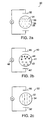
- the display media 12 can comprise a plurality of bichromal spheres shown in Figure 3.
- a bichromal sphere 60 typically comprises a positively charged hemisphere 62 of a first color and a negatively charged hemisphere 64 of a second color in a liquid medium 66.
- the sphere 60 rotates and displays the color of one of the two hemispheres 62, 64.
- the display media 71 is sandwiched between two pieces of glass 72, 72' as shown in Figure 4.
- Each piece of glass has an etched, clear electrode structure 74, 74' formed using indium tin oxide.
- the first electrode 74 controls the pixels of the display 70 that may be addressed, that is changed from one visible state to another.
- a second electrode 74' sometimes called a counter electrode, addresses all the display pixels as one large electrode, and is generally designed so that the placement of the rear electrode wire connections do not produce any unwanted visible changes in the appearance of the display medium.
- the transistors 75 are connected to the first electrodes 74.
- the second electrode 74' can also be patterned to control specific segments of the displays 70.
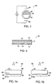
- Electrodes 82, 82' are disposed on only one side of a display 80, allowing the display 80 to be rear-addressed without a front electrode. Utilizing only one side of the display 80 for electrodes 82, 82' simplifies fabrication of displays 80. For example, if the electrodes 82, 82' are disposed on only the rear side of a display 80, both of the electrodes 82, 82' can be fabricated using opaque materials, because the electrodes 82, 82' do not need to be transparent.
- Figure 5a depicts a single capsule 84 of an encapsulated display media.
- the embodiment depicted in Figure 5a includes a capsule 84 containing at least one particle 86 dispersed in a suspending fluid 88.
- the capsule 84 is addressed by a first electrode 82 and a second electrode 82'.
- the first electrode 82 is smaller than the second electrode 82'.
- the first electrode 82 and the second electrode 82' may be set to voltage potentials which affect the position of the particles 86 in the capsule 84.
- a transistor 89 is connected to the first electrode 82.
- the electrodes 82, 82' should be sized and positioned appropriately so that together they address the entire capsule 84. There may be exactly one pair of electrodes 82, 82' per capsule 84, multiple pairs of electrodes per capsule 84, or a single pair of electrodes may span multiple capsules 84. In the embodiment shown in Figures 5a and 5b, the capsule 84 has a flattened, rectangular shape. In these embodiments, the electrodes 82, 82' should address most, or all, of the flattened surface area adjacent the electrodes 82, 82'. The smaller electrode 82 is at most one-half the size of the larger electrode 82'.
- the smaller electrode 82 is one-quarter the size of the larger electrode 82'; in more preferred embodiments the smaller electrode 82 is one-eighth the size of the larger electrode 82'. In even more preferred embodiments, the smaller electrode 82 is one-sixteenth the size of the larger electrode 82'. It should be noted that reference to "smaller" in connection with the electrode 82 means that the electrode 82 addresses a smaller amount of the surface area of the capsule 84, not necessarily that the electrode 82 is physically smaller than the larger electrode 82'. For example, multiple capsules may be positioned such that less of each capsule is addressed by the "smaller" electrode, even though both electrodes are equal in size.
- Electrodes may be fabricated from any material capable of conducting electricity so that electrode 82, 82' may apply an electric field to the capsule 84.
- the rear-addressed embodiments depicted in Figures 5a and 5b allow the electrodes 82, 82' to be fabricated from opaque materials such as solder paste, copper, copper-clad polyimide, graphite inks, silver inks and other metal-containing conductive inks.
- electrodes may be fabricated using transparent materials such as indium tin oxide and conductive polymers such as polyanifine or polythiophenes.
- Electrodes 82, 82' may be provided with contrasting optical properties. In some embodiments, one of the electrodes has an optical property complementary to optical properties of the particles 86.
- the transistor 90 comprises an organic-based field effect transistor.
- An organic-based field effect transistor 90 includes a substrate 92, , a gate electrode 96 disposed adjacent the substrate 92, a dielectric layer 94 disposed adjacent the gate electrode 96, an organic semiconductor 97 disposed adjacent the dielectric layer 94, and a source electrode 98 and a drain electrode 99 disposed adjacent the dielectric layer 94 and in contact with the semiconductor layer 97.
- the substrate 92 for example, can comprise an insulator such as undoped silicon, glass, or plastic.
- the substrate can be patterned to serve as an electrode, which can be in electrical connection with a pixel electrode, or itself serve as the pixel electrode.
- the gate electrode 96, the source electrode 98, and the drain electrode 99 can comprise a metal such as gold.
- the electrodes 96, 98 and 99 can comprise a conductive polymer such as polythiophene or polyaniline, a printed conductor such as a polymer film comprising metal particles such as silver or nickel, a printed conductor comprising a polymer film containing graphite or some other conductive carbon material, or a conductive oxide such as tin oxide or indium tin oxide, or metal electrodes such as aluminum or gold.
- the dielectric layer 94 for example, can comprise a silicon dioxide layer.
- the dielectric layer 94 can comprise an insulating polymer such as polyimide and its derivatives, an inorganic oxide, an inorganic nitride such as silicon nitride, or an inorganic/organic composite material such as an organic-substituted silicon oxide, or a sol-gel organosilicon glass.
- an insulating polymer such as polyimide and its derivatives
- an inorganic oxide such as silicon nitride
- an inorganic/organic composite material such as an organic-substituted silicon oxide, or a sol-gel organosilicon glass.
- Figure 6b provides another configuration of an organic-based field effect transistor 90'.
- the transistor 90' includes a substrate 92', a gate electrode 96' provided on the substrate 92', a dielectric layer 94' provided on the gate electrode 96', an organic semiconductor 97' provided on the dielectric layer 94', and a source electrode 98' and a drain electrode 99' provided on the organic semiconductor 97'.
- the substrate 92' can comprise polyester, or some other film-based polymer.
- the substrate 92' can be a metal foil insulated from the gate electrode by a non-conducting material.
- the gate electrode 96' can comprise Indium Tin Oxide or a conducting polymer such as polyaniline.
- the dielectric layer 94' can comprise polyimide.
- field effect transistor configurations provided in Figures 6a and 6b are exemplary only. Other transistor designs known to those skilled in the art can be used in accordance with the present invention.
- a top gate structure in which the source and drain electrodes are placed adjacent the substrate, covered by the dielectric layer, which in turn is covered by the semiconductor and gate electrode, can also be used in accordance with the present invention.
- each transistor 100 is electrically connected to a pixel electrode 102, a column electrode 104, and a row electrode 106.
- the pixel electrode 102 is connected to the drain of the transistor 100.
- the column electrode 104 is connected to the source of the transistor 100.
- the row electrode 106 is connected to the gate of the transistor 100.
- transistors sharing a common gate electrode are activated.
- the conductive substrate can be patterned such that a voltage is applied to the transistors in a common row or a common column only. Alternatively, if the transistors are spaced far enough apart or if the conductivity of the substrate is poor, than a voltage placed on the gate electrode will only provide enough voltage to activate nearby transistors.
- the organic semiconductor comprises a polymeric or oligomeric semiconductor.
- suitable polymeric semiconductors include, but are not limited to, polythiophene, poly(3-alkyl), alkyl-substituted oligothiophene, polythienylenevinylene, poly(para-phenylenevinylene) and doped versions of these polymers.
- An example of suitable oligomeric semiconductor is alpha-hexathienylene. Horowitz, Organic Field-Effect Transistors, Adv. Mater., 10, No. 5, p. 365 (1998) describes the use of unsubstituted and alkyl-substituted oligothiophenes in transistors.
- a field effect transistor made with regioregular poly(3-hexylthiophene) as the semiconductor layer is described in Bao et al., Soluble and Processable Regioregular Poly(3-hexylthiophene) for Thin Film Field-Effect Transistor Applications with High Mobility, Appl. Phys. Lett. 69 (26), p. 4108 (December 1996).
- a field effect transistor made with ⁇ -hexathienylene is described in U.S. Patent No. 5,659,181.
- the organic semiconductor 90, 90' comprises a carbon based compound.
- suitable carbon based compounds include, but are not limited to, pentacene, phthalocyanine, benzodithiophene, fullerene, buckminsterfullerene, tetracyanonaphthoquinone, and tetrakisimethylanimoethylene.
- the display is addressed in the following manner. While a voltage is applied to the gate electrodes on a row, different voltages are applied to each column electrode so that each pixel in that row is driven to a unique state. The characteristics of the transistors prevent pixels on other rows from responding to the column voltages. Each row electrode (gate line) is then scanned in sequence, so that an image can be built up across the entire display.
- the electronic display comprises an irregular grouping of pixels and electrodes, rather than a regular x-y grid of electrodes and pixels.
- an organic-based field effect transistor is protected by a barrier layer.
- the barrier layer protects the transistor from air, water, light or other environmental factors to which the transistor can be sensitive.
- the barrier layer also protects the transistor from the solvent of the display media, if necessary. Where the solvent of the display media has a different polarity from the transistor material, contact between the solvent and the transistor may not affect the transistor properties. However, where the solvent would affect the properties of the transistor upon contact, the barrier layer segregates the solvent and the transistor.
- the barrier layer is opaque.
- the barrier layer comprises a metal film such as an aluminum film.
- the barrier layer comprises a metal oxide coating such as Indium Oxide, Tin Oxide, Indium Tin Oxide, Silicon Monoxide, or Silicon Dioxide coatings.
- a metal film layer or a conducting oxide film layer may require additional insulating layers to prevent unwanted electrical connections between transistor components.
- the barrier layer comprises a polymeric film containing fluorine.
- the barrier layer comprises a polymeric film containing absorbing particles or dyes.
- the barrier layer comprises multiple layers of materials including metal and/or insulator.
- the barrier layer can comprise a multi layer polymer composite film.
- each transistor 90' is individually protected from the display media 93 by a barrier layer 110.
- Each transistor 90' is positioned adjacent a pixel electrode 124 on a substrate 92'.
- the column electrode 123, and the row electrode (not shown) are also provided on the substrate 92'.
- the barrier layer 110 is positioned over at least the semiconductor layer 97' of the transistor 90' which would otherwise be exposed to the display media 93. Alternatively, the barrier layer 110 can protect the entire transistor 90'.
- the source electrode 98' is connected to the column electrode 123.
- the drain electrode 99' is connected to the pixel electrode 124.
- the gate electrode 96' is connected to the row electrode (not shown).
- an array of transistors 130 are protected from the display media 132 with a first barrier layer 133.
- the array of transistors 130 are positioned on a substrate and placed underneath the pixel electrodes 134.
- the substrate 135 also functions as a second barrier layer, protecting the transistors 130 from the environment.
- the edges of the first barrier layer 133 and the second barrier layer are sealed, thereby forming a barrier capsule 136 encapsulating the array of transistors 130.
- the barrier capsule 136 also encapsulates the column electrodes 138 and the row electrodes (not shown).
- the first barrier layer 133 includes a plurality of vias for providing an electrical contact between a transistor 130 and its adjacent pixel electrode 134.
- the vias can be made by etching the first barrier layer 133 to provide a plurality of opening and providing a conductive material inside the openings, thereby providing electrical contact between the drain electrode 137 of the transistor 130 and the pixel electrode 134.
- An electronic display comprising a microencapsulated particle-based display media and an organic-based field effect transistor offer numerous advantages.
- the display can be made inexpensively using a simple manufacturing process.
- both the organic-based field effect transistor and the display media can be printed.
- the performance requirements for the organic-based field effect transistor when used in this particle-based display is not stringent. Because of low current requirements of the particle-based encapsulated display media, transistors having moderate performance characteristic (i.e., transistor mobility of less than 10 -3 cm 2 /Vs) can be suitable for driving such display.
- moderate performance characteristic i.e., transistor mobility of less than 10 -3 cm 2 /Vs
- the underlying substrate need not be transparent. This offers significant design advantages for the combination of organic-based transistors and microencapsulated particle-based displays.
- the transistor can be as large as the pixel itself.
- the organic transistor need not address the display continuously, which will extend the life of the transistor.
- a microencapsulated particle-based display media prevents fluid from the display media from coming in contact with the transistor device, and provides additional stability for the transistor.
- a display is created by printing the entire display or a portion of the display.
- printing is intended to include all forms of printing and coating, including: premetered coating such as patch die coating, slot or extrusion coating, slide or cascade coating, and curtain coating; roll coating such as knife over roll coating, forward and reverse roll coating; gravure coating; dip coating; spray coating; meniscus coating; spin coating; brush coating; air knife coating; silk screen printing processes; electrostatic printing processes; thermal printing processes; and other similar techniques.
- the display is manufactured by providing conductive coatings to form column electrodes, row electrodes, and pixel electrodes on a substrate, providing organic-based transistors on the substrate, printing an electronic ink comprising a plurality of encapsulated display media on the substrate, and printing a second conductive coating on the electronic ink.
- the conductive coatings can be provided by printing, evaporation, or sputtering, or using any other suitable method known to those skilled in the art.
- the conductive coatings may be Indium Tin Oxide (ITO) or some other suitable conductive material.
- the conductive coatings may be applied from a vaporous phase, by electrolytic reaction, or deposition from a dispersed state such as spray droplets or dispersions in liquids.
- the conductive coatings need not be the same conductive material.
- Printable electrode structures for displays are described in commonly owned U.S. Patent Application Serial Number 09/141,103, filed on August 27, 1998, incorporated herein by reference.
- the substrate is a polyester sheet.
- the electronic ink can be printed in a variety of ways including screen printing, ink jet printing, and deposition. Details of these printing methods are described in commonly owned U.S. Patent Application Serial Number 08/935,800 filed on September 23, 1997, incorporated herein by reference.
- the organic-based transistor is also printed in its entirety.
- an organic-based transistor comprising electrodes based on ITO or polymeric conductor, a polymeric dielectric layer, and a polymeric semiconductor can be fabricated by printing.
- Bao et al., High-Performance Plastic Transistors Fabricated by Printing Techniques, Chem. Mater. 1997, 9, 1299-1301 describes an organic-based transistor made by printing.
- an organic semiconductor of the organic transistor can be made using a solvent-assisted printing step.
- the polymer material to be printed is dissolved in a solvent, and the solution containing the polymer and the solvent is printed on the electrode. Subsequently, the solvent evaporates and leaves behind the polymer material.
- the solvent may evaporate at room temperature or at an elevated temperature, under vacuum, under exposure to a stream of air, or a combination of the above.
- the organic-based transistor is fabricated using a combination of a variety of methods.
- the organic semiconductor layer can be provided using evaporation.
- evaporation the material to be deposited is typically placed in a container and is heated under reduced pressure, vaporizing the molecules.
- the vaporized molecules strike a substrate and forms a coating on the substrate.
- the electrodes and leads of the transistor can be fabricated by printing, coating, evaporation, and/or photolithography.
- the dielectric layer can be fabricated using any of the above described methods.
- the organic transistor is protected by a barrier layer.
- the transistor can be protected by coating the transistor with a film comprising the barrier layer material.
- the barrier layer can comprises a metal film, a metal oxide coating or a polymeric film.
- the transistor can be protected by laminating the transistor and the barrier layer, printing the barrier layer on the transistors, solvent coating the barrier layer on the transistors, or evaporating or sputtering the barrier layer on the transistors.
- an array of organic-based transistors can be encapsulated in a barrier capsule.
- the barrier capsule can be formed by providing a first barrier layer over the transistors, a second barrier layer under the transistors, and sealing the edges of the first and second barrier layers.
- the first barrier layer can be printed, coated, evaporated or sputtered on the transistors.
- the second barrier layer can comprise a substrate on which the transistors are formed.
- Other suitable methods known to those skilled in the art can be used to encapsulate the organic-based transistors in a barrier capsule. These various methods are well known to those skilled in the art.
- the organic-based transistors are fabricated on a first substrate, and the electronic ink is fabricated on a second substrate. Subsequently, the two substrates are laminated together to form a display device.
Landscapes
- Physics & Mathematics (AREA)
- Nonlinear Science (AREA)
- General Physics & Mathematics (AREA)
- Engineering & Computer Science (AREA)
- Optics & Photonics (AREA)
- Chemical & Material Sciences (AREA)
- Crystallography & Structural Chemistry (AREA)
- Mathematical Physics (AREA)
- Molecular Biology (AREA)
- Nanotechnology (AREA)
- Microelectronics & Electronic Packaging (AREA)
- Power Engineering (AREA)
- Health & Medical Sciences (AREA)
- Life Sciences & Earth Sciences (AREA)
- Theoretical Computer Science (AREA)
- Condensed Matter Physics & Semiconductors (AREA)
- Chemical Kinetics & Catalysis (AREA)
- Computer Hardware Design (AREA)
- Electrochemistry (AREA)
- Thin Film Transistor (AREA)
- Electrochromic Elements, Electrophoresis, Or Variable Reflection Or Absorption Elements (AREA)
- Liquid Crystal (AREA)
Abstract
Description
- This invention claims priority to provisional applications U.S.S.N. 60/081,374 filed on April 10, 1998 and U.S.S.N. 60/096,302 filed on August 12, 1998.
- This invention generally relates to electronic displays and more specifically to electronic displays addressed by organic-based field effect transistors.
- Microencapsulated, particle-based displays can be made highly reflective, bistable, and optically and electrically efficient. To obtain a high resolution display, however, individual pixels of a display must be addressable without interference from adjacent pixels. One way to achieve this objective is to provide an array of nonlinear transistor elements, where one transistor is associated with each pixel. The addressing electrodes are connected to the pixel through the transistor.
- Most examples of nonlinear elements to date have been fabricated using vacuum-deposited silicon on glass. This process is costly in addition to being complex. The complexity prevents large area devices from being readily constructed. In addition, it is difficult to create silicon transistors on plastic or other flexible film.
- Recently, there has been significant development in the area of organic semiconducting polymers and molecules. Thin film transistors have been made out of semiconducting polymers. See Bao et al., Soluble and Processable Regioregular Poly(3-hexylthiophene) for Thin Film Field-Effector Transistor Applications with High Mobility, Appl. Phys. Lett. 69(26), 4108 (December 1996); and Bao et al., High-Performance Plastic Transistors Fabricated by Printing Techniques, Chem. Mater. 1997, 9, 1299. U.S. Patent No. 5,574,291 describes addressing liquid crystal displays with transistors made out of semiconducting polymers. While remarkable advances have been made in the performance of organic-based transistors, the mobility characteristics of many organic semiconductor materials and devices are insufficient to successfully drive many types of liquid crystal or emissive displays. Therefore, many organic-based transistors are not suitable for use with liquid crystal displays.
- In addition, liquid crystals can degrade the transistors when they come in contact with the transistors. Many organic semiconductor materials can be swollen by, or dissolved by, liquid crystalline fluids because those fluids are good solvents. This solvent compatibility makes it challenging to design systems in which organic transistor devices can remain stable while in contact with or close proximity to liquid crystalline solvents, limiting their viability.
- In one aspect, the invention features a display. The display comprises an encapsulated display media and an organic-based field effect transistor. The display media comprises a plurality of particles and a fluid, the display media has a first surface and a second surface. The organic-based field effect transistor comprises an organic semiconductor. The organic-based field effect transistor is disposed adjacent the second surface of the display media for addressing the display media. The display media can comprise a plurality of microencapsulated electrophoretic particles, suspended particles, or rotating balls.
- In one embodiment, the organic semiconductor of the transistor comprises a polymeric and/or oligomeric semiconductor. For example, the polymeric semiconductor can comprise polythiophene, poly(3-alkyl)thiophene, alkyl-substituted oligothiophene, polythienylenevinylene, or poly(para-phenylenevinylene). For example, the oligomeric semiconductor can comprise alpha-hexathienylene. In another embodiment, the organic semiconductor can be selected from a group consisting of pentacene, phthalocyanine, benzodithiophene, fullerene, buckminsterfullerene, tetracyanonaphthoquinone, and tetrakisimethylanimoethylene, and derivatives.
- In one embodiment, the display further comprises a barrier layer disposed adjacent at least a portion of the organic-based field effect transistor. In one detailed embodiment, the display comprises a plurality of pixel electrodes disposed adjacent the second surface of the display media and an array of transistors, each transistor protected with a barrier layer disposed adjacent the transistor. In another detailed embodiment, the display comprises an array of transistors encapsulated in a barrier capsule and disposed adjacent the second surface of the display media such that each transistor is connected to a pixel electrode.
- The barrier layer or capsule can comprise a metal film, a metal oxide coating, a polymeric coating or a combination of these materials. In particular, a barrier layer or capsule comprising a metal film will also comprise an insulating coating to prevent unwanted electrical connections between the barrier capsule or layer and the transistor. The barrier layer or capsule can protect the transistor from light such as visible light or ultraviolet light. The barrier layer or capsule can protect the transistor from oxygen or moisture. In addition, the barrier layer or capsule can protect the transistor from solvents or other chemicals. In another embodiment, the organic-based field effect transistors are disposed on a substrate. The substrate can be opaque. The substrate can protect the transistors from oxygen or moisture.
- In another aspect, the invention features a method of manufacturing a display. The method comprises the steps of: (a) providing an encapsulated display media comprising a plurality of particles and a fluid, the display media having a first surface and a second surface; and (b) providing an organic-based field effect transistor array comprising an organic semiconductor adjacent the second surface of the display media.
- In one embodiment, step a) comprises providing an encapsulated display media on a first substrate; and step b) comprises (b1) providing an organic-based field effect transistor array on a second substrate, and (b2) combining the display media and the organic-based field effect transistor array to form the display.
- In one embodiment, step (b) comprises printing the organic-based field effect transistor array. In one detailed embodiment, step (b) comprises printing the organic-based field effect transistor array using a solvent assisted printing step. In one embodiment, step (a) comprises providing a display media comprising microencapsulated electrophoretic particles, suspended particles, or rotating balls.
- In another embodiment, step (b) comprises providing an organic-based field effect transistor array comprising a polymeric or oligomeric semiconductor. For example, the polymeric semiconductor can comprise polythiophene, poly(3-alkyl)thiophene, alkyl-substituted oligothiophene, polythienylenevinylene, or poly(para-phenylenevinylene). For example, the oligomeric semiconductor can comprise alpha-hexathienylene. In another embodiment, the organic semiconductor is selected from a group consisting of pentacene, phthalocyanine, benzodithiophene, fullerene, buckminsterfullerene, tetracyanonaphthoquinone, and tetrakisimethylanimoethylene.
- In another embodiment, step (b) comprises (b1) providing an organic-based field effect transistor array, and (b2) providing a barrier layer over each organic-based field effect transistor of the array to protect the transistor. In another embodiment, step (a) comprises (a1) providing a display media and (a2) providing a plurality of pixel electrodes adjacent the second surface of the display media; and step (b) comprises (b1) encapsulating the transistor array in a barrier capsule and step (b2) disposing the encapsulated transistor array adjacent the display media such that each transistor is disposed adjacent a pixel electrode. The barrier layer or capsule can comprise a metal film, a metal oxide coating, or a polymeric coating. The barrier layer or capsule can protect the transistor from light such as visible light or ultraviolet light. The barrier layer or capsule can protect the transistor from oxygen or moisture. The barrier layer or capsule can further protect the transistor from a solvent.
- In another embodiment, step (b) comprises providing an organic transistor array by evaporating the organic semiconductor. In another embodiment, step (b) comprises providing an organic transistor array by solvent coating an insulator of the transistors. In still another embodiment, step (b) comprises providing an organic transistor array by evaporating conductive leads to the transistors.
- The foregoing and other objects, features and advantages of the present invention, as well as the invention itself, will be more fully understood from the following description of preferred embodiments, when read together with the accompanying drawings, in which:
- Figure 1a shows a cross section view of an electronic display according to one embodiment of the present invention.
- Figure 1b shows a cross section view of an electronic display according to another embodiment of the present invention.
- Figure 1c shows a top view of the electronic display of Figure 1b with the display media and the first electrode removed.
- Figure 2a shows a cross section view of an electronic ink according to one embodiment of the present invention.
- Figure 2b shows a cross section view of an electronic ink according to another embodiment of the present invention.
- Figure 2c shows a cross section view of an electronic ink according to another embodiment of the present invention.
- Figure 3 shows a cross section view of a bichromal sphere according to one embodiment of the present invention.
- Figure 4 shows a cross section view of a means for addressing an electronic display according to one embodiment of the present invention.
- Figures 5a and 5b show cross section views of a means for addressing an electronic display according to another embodiment of the present invention.
- Figures 6a shows a cross section view of an organic-based field effect transistor according to one embodiment of the present invention.
- Figures 6b shows a cross section view of an organic-based field effect transistor according to one embodiment of the present invention.
- Figures 7 illustrates connections between a transistor and electrodes of an electronic display.
- Figure 8 shows a cross section view of an organic-based field effect transistor according to one embodiment of the present invention.
- Figure 9 shows a cross section view of an electronic display according to one embodiment of the present invention.
- Figure 10 shows a cross section view of an electronic display according to one embodiment of the present invention.
-
- Referring to Figure 1a, an
electronic display 10 includes adisplay media 12, afirst electrode 16, asecond electrode 18, an array oftransistors 20, an array ofrow electrodes 17, and an array ofcolumn electrodes 15. Thefirst electrode 16 is disposed on afirst surface 11 of thedisplay media 12. In one embodiment, thefirst electrode 16 comprises a transparent, continuous electrode. Thesecond electrode 18 disposed on asecond surface 13 of thedisplay media 12 comprises an array of patternedpixel electrodes 18. Each patternedelectrode 18 defines a pixel of thedisplay 10. Thetransistors 20 are located underneath thepixel electrodes 18. Eachtransistor 20 is electrically connected to apixel electrode 18 to address a pixel. Arow electrode 17 is electrically connected to all thetransistors 20 in that row. Acolumn electrode 15 is electrically connected to all thetransistors 20 in that column. - In the embodiment of Figure 1a, the
transistors 20 are located on the backside of thedisplay 10 from the standpoint of theviewer 19. Alternatively, thetransistors 20 can be located on the front side of thedisplay 10. In this embodiment, transparent pixel electrodes would be positioned on thefirst surface 11 of thedisplay media 12, while the continuous electrode would be positioned on thesecond surface 13 of thedisplay media 12. The continuous electrode need not be transparent. - In one embodiment, the
electronic display 10 can be reflective. In this embodiment, the size of thetransistors 20 positioned on the backside of thedisplay 10 does not affect the ability of theviewer 19 to view thedisplay 10. Therefore, the size of thetransistor 20 can be determined based on manufacturing considerations and transistor performance. The size of thetransistor 20 can be in the range from about 1% to about 100% of the area of the pixel thetransistor 20 addresses. In another embodiment, theelectronic display 10 can be transmissive. In this embodiment, thetransistors 20 can impede the ability of theviewer 19 to view thedisplay 10. Therefore, thetransistors 20 are made as small as possible. In one embodiment, the size of thetransistor 20 is less than 50% of the area of the pixel addressed by thetransistor 20. In a preferred embodiment, the size of thetransistor 20 is less than 20% of the area of the pixel addressed by thetransistor 20. In a more preferred embodiment, the size of thetransistor 20 is less than 5% of the area of the pixel addressed by thetransistor 20. - Referring to Figures 1b and 1c, an electronic display 10' includes a display media 12' having a plurality of pixels defined by the second electrodes 18'. The display 10' further includes the first electrode 16', the transistors 20', the row electrodes 17', the
column electrodes 15', and aninsulator 21. In this embodiment, the transistors 20' are positioned adjacent the pixel electrodes 18'. - In one embodiment, the
display media 12 comprises a particle-based display media. In one detailed embodiment, the particle-based display media comprises an electronic ink. An electronic ink is an optoelectronically active material which comprises at least two phases: an electrophoretic contrast media phase and a coating/binding phase. The electrophoretic phase comprises, in some embodiments, a single species of electrophoretic particles dispersed in a clear or dyed medium, or more than one species of electrophoretic particles having distinct physical and electrical characteristics dispersed in a clear or dyed medium. In some embodiments the electrophoretic phase is encapsulated, that is, there is a capsule wall phase between the two phases. The coating/binding phase includes, in one embodiment, a polymer matrix that surrounds the electrophoretic phase. In this embodiment, the polymer in the polymeric binder is capable of being dried, crosslinked, or otherwise cured as in traditional inks, and therefore a printing process can be used to deposit the electronic ink onto a substrate. - The optical quality of an electronic ink is quite distinct from other electronic display materials. The most notable difference is that the electronic ink provides a high degree of both reflectance and contrast because it is pigment based (as are ordinary printing inks). The light scattered from the electronic ink comes from a very thin layer of pigment close to the top of the viewing surface. In this respect it resembles an ordinary, printed image. Also, electronic ink is easily viewed from a wide range of viewing angles in the same manner as a printed page, and such ink approximates a Lambertian contrast curve more closely than any other electronic display material. Since electronic ink can be printed, it can be included on the same surface with any other printed material, including traditional inks. Electronic ink can be made optically stable in all display configurations, that is, the ink can be set to a persistent optical state. Fabrication of a display by printing an electronic ink is particularly useful in low power applications because of this stability.
- Electronic ink displays are novel in that they can be addressed by DC voltages and draw very little current. As such, the conductive leads and electrodes used to deliver the voltage to electronic ink displays can be of relatively high resistivity. The ability to use resistive conductors substantially widens the number and type of materials that can be used as conductors in electronic ink displays. In particular, the use of costly vacuum-sputtered indium tin oxide (ITO) conductors, a standard material in liquid crystal devices, is not required. Aside from cost savings, the replacement of ITO with other materials can provide benefits in appearance, processing capabilities (printed conductors), flexibility, and durability. Additionally, the printed electrodes are in contact only with a solid binder, not with a fluid layer (like liquid crystals). This means that some conductive materials, which would otherwise dissolve or be degraded by contact with liquid crystals, can be used in an electronic ink application. These include opaque metallic inks for the rear electrode (e.g., silver and graphite inks), as well as conductive transparent inks for either substrate. These conductive coatings include conducting or semiconducting colloids, examples of which are indium tin oxide and antimony-doped tin oxide. Organic conductors (polymeric conductors and molecular organic conductors) also may be used. Polymers include, but are not limited to, polyaniline and derivatives, polythiophene and derivatives, poly3,4-ethylenedioxythiophene (PEDOT) and derivatives, polypyrrole and derivatives, and polyphenylenevinylene (PPV) and derivatives. Organic molecular conductors include, but are not limited to, derivatives of naphthalene, phthalocyanine, and pentacene. Polymer layers can be made thinner and more transparent than with traditional displays because conductivity requirements are not as stringent.
- Figure 2a shows an
electrophoretic display 30. Thebinder 32 includes at least onecapsule 34, which is filled with a plurality ofparticles 36 and a dyed suspendingfluid 38. In one embodiment, theparticles 36 are titania particles. When a direct-current electric field of the appropriate polarity is applied across thecapsule 34, theparticles 36 move to the viewed surface of the display and scatter light. When the applied electric field is reversed, theparticles 36 move to the rear surface of the display and the viewed surface of the display then appears dark. - Figure 2b shows another
electrophoretic display 40. This display comprises a first set ofparticles 42 and a second set ofparticles 44 in acapsule 41. The first set ofparticles 42 and the second set ofparticles 44 have contrasting optical properties. For example, the first set ofparticles 42 and the second set ofparticles 44 can have differing electrophoretic mobilities. In addition, the first set ofparticles 42 and the second set ofparticles 44 can have contrasting colors. For example, the first set ofparticles 42 can be white, while the second set ofparticles 44 can be black. Thecapsule 41 further includes a substantially clear fluid. Thecapsule 41 haselectrodes 46 and 46' disposed adjacent it. Theelectrodes 46, 46' are connected to a source ofvoltage 48, which may provide an alternating-current (AC) field or a direct-current (DC) field to thecapsule 41. Upon application of an electric field across theelectrodes 46, 46', the first set ofparticles 42 move toward electrode 46', while the second set ofparticles 44 move towardelectrode 46. - Figure 2c shows a suspended
particle display 50. The suspendedparticle display 50 includes needle-like particles 52 in atransparent fluid 54. Theparticles 52 change their orientation upon application of an AC field across theelectrodes 56, 56'. When the AC field is applied, theparticles 52 are oriented perpendicular with respect to the display surface and the display appears transparent. When the AC field is removed, theparticles 52 are randomly oriented and thedisplay 50 appears opaque. - The electrophoretic displays provided in Figures 2a-2c are exemplary only, and other electrophoretic displays can be used in accordance with the present invention. Other examples of electrophoretic displays are described in commonly owned, copending U.S. Patent Application Serial Numbers 08/935,800 and 09/140,792 which are incorporated herein by reference.
- In another detailed embodiment, the
display media 12 can comprise a plurality of bichromal spheres shown in Figure 3. Abichromal sphere 60 typically comprises a positively chargedhemisphere 62 of a first color and a negatively chargedhemisphere 64 of a second color in aliquid medium 66. Upon application of an electric field across thesphere 60 through a pair ofelectrodes 68, 68', thesphere 60 rotates and displays the color of one of the twohemispheres - An electronic display can be addressed in a variety of ways. In one embodiment, the
display media 71 is sandwiched between two pieces ofglass 72, 72' as shown in Figure 4. Each piece of glass has an etched,clear electrode structure 74, 74' formed using indium tin oxide. Thefirst electrode 74 controls the pixels of thedisplay 70 that may be addressed, that is changed from one visible state to another. A second electrode 74', sometimes called a counter electrode, addresses all the display pixels as one large electrode, and is generally designed so that the placement of the rear electrode wire connections do not produce any unwanted visible changes in the appearance of the display medium. In this embodiment, thetransistors 75 are connected to thefirst electrodes 74. Alternatively, the second electrode 74' can also be patterned to control specific segments of thedisplays 70. - An alternate means for addressing an encapsulated electrophoretic display (or other display) structure is also described in Figures 5a and 5b. In this embodiment,
electrodes 82, 82' are disposed on only one side of adisplay 80, allowing thedisplay 80 to be rear-addressed without a front electrode. Utilizing only one side of thedisplay 80 forelectrodes 82, 82' simplifies fabrication ofdisplays 80. For example, if theelectrodes 82, 82' are disposed on only the rear side of adisplay 80, both of theelectrodes 82, 82' can be fabricated using opaque materials, because theelectrodes 82, 82' do not need to be transparent. - Figure 5a depicts a
single capsule 84 of an encapsulated display media. In brief overview, the embodiment depicted in Figure 5a includes acapsule 84 containing at least oneparticle 86 dispersed in a suspendingfluid 88. Thecapsule 84 is addressed by afirst electrode 82 and a second electrode 82'. Thefirst electrode 82 is smaller than the second electrode 82'. Thefirst electrode 82 and the second electrode 82' may be set to voltage potentials which affect the position of theparticles 86 in thecapsule 84. Atransistor 89 is connected to thefirst electrode 82. - The
electrodes 82, 82' should be sized and positioned appropriately so that together they address theentire capsule 84. There may be exactly one pair ofelectrodes 82, 82' percapsule 84, multiple pairs of electrodes percapsule 84, or a single pair of electrodes may spanmultiple capsules 84. In the embodiment shown in Figures 5a and 5b, thecapsule 84 has a flattened, rectangular shape. In these embodiments, theelectrodes 82, 82' should address most, or all, of the flattened surface area adjacent theelectrodes 82, 82'. Thesmaller electrode 82 is at most one-half the size of the larger electrode 82'. In preferred embodiments thesmaller electrode 82 is one-quarter the size of the larger electrode 82'; in more preferred embodiments thesmaller electrode 82 is one-eighth the size of the larger electrode 82'. In even more preferred embodiments, thesmaller electrode 82 is one-sixteenth the size of the larger electrode 82'. It should be noted that reference to "smaller" in connection with theelectrode 82 means that theelectrode 82 addresses a smaller amount of the surface area of thecapsule 84, not necessarily that theelectrode 82 is physically smaller than the larger electrode 82'. For example, multiple capsules may be positioned such that less of each capsule is addressed by the "smaller" electrode, even though both electrodes are equal in size. - Electrodes may be fabricated from any material capable of conducting electricity so that
electrode 82, 82' may apply an electric field to thecapsule 84. As noted above, the rear-addressed embodiments depicted in Figures 5a and 5b allow theelectrodes 82, 82' to be fabricated from opaque materials such as solder paste, copper, copper-clad polyimide, graphite inks, silver inks and other metal-containing conductive inks. Alternatively, electrodes may be fabricated using transparent materials such as indium tin oxide and conductive polymers such as polyanifine or polythiophenes.Electrodes 82, 82' may be provided with contrasting optical properties. In some embodiments, one of the electrodes has an optical property complementary to optical properties of theparticles 86. - The means of addressing an electronic display provided in Figures 4, and Figures 5a and 5b are exemplary only. Other means of addressing an electronic display can be used in accordance with the present invention. Other means of addressing an electronic display are described in commonly-owned, copending U.S. Patent Application Serial Number 09/141,280, which is incorporated herein by reference.
- Referring to Figure 6a, the
transistor 90 comprises an organic-based field effect transistor. An organic-basedfield effect transistor 90 includes asubstrate 92, , agate electrode 96 disposed adjacent thesubstrate 92, adielectric layer 94 disposed adjacent thegate electrode 96, anorganic semiconductor 97 disposed adjacent thedielectric layer 94, and asource electrode 98 and adrain electrode 99 disposed adjacent thedielectric layer 94 and in contact with thesemiconductor layer 97. Thesubstrate 92, for example, can comprise an insulator such as undoped silicon, glass, or plastic. Alternatively, the substrate can be patterned to serve as an electrode, which can be in electrical connection with a pixel electrode, or itself serve as the pixel electrode. Thegate electrode 96, thesource electrode 98, and thedrain electrode 99, can comprise a metal such as gold. Alternatively, theelectrodes dielectric layer 94, for example, can comprise a silicon dioxide layer. Alternatively, thedielectric layer 94 can comprise an insulating polymer such as polyimide and its derivatives, an inorganic oxide, an inorganic nitride such as silicon nitride, or an inorganic/organic composite material such as an organic-substituted silicon oxide, or a sol-gel organosilicon glass. - Figure 6b provides another configuration of an organic-based field effect transistor 90'. The transistor 90' includes a substrate 92', a gate electrode 96' provided on the substrate 92', a dielectric layer 94' provided on the gate electrode 96', an organic semiconductor 97' provided on the dielectric layer 94', and a
source electrode 98' and a drain electrode 99' provided on the organic semiconductor 97'. For example, the substrate 92' can comprise polyester, or some other film-based polymer. Alternatively, the substrate 92' can be a metal foil insulated from the gate electrode by a non-conducting material. The gate electrode 96' can comprise Indium Tin Oxide or a conducting polymer such as polyaniline. The dielectric layer 94' can comprise polyimide. The field effect transistor configurations provided in Figures 6a and 6b are exemplary only. Other transistor designs known to those skilled in the art can be used in accordance with the present invention. For example, a top gate structure in which the source and drain electrodes are placed adjacent the substrate, covered by the dielectric layer, which in turn is covered by the semiconductor and gate electrode, can also be used in accordance with the present invention. - Referring to Figure 7, each
transistor 100 is electrically connected to apixel electrode 102, acolumn electrode 104, and arow electrode 106. Thepixel electrode 102 is connected to the drain of thetransistor 100. Thecolumn electrode 104 is connected to the source of thetransistor 100. Therow electrode 106 is connected to the gate of thetransistor 100. - In one embodiment, transistors sharing a common gate electrode are activated. The conductive substrate can be patterned such that a voltage is applied to the transistors in a common row or a common column only. Alternatively, if the transistors are spaced far enough apart or if the conductivity of the substrate is poor, than a voltage placed on the gate electrode will only provide enough voltage to activate nearby transistors.
- In one embodiment, the organic semiconductor comprises a polymeric or oligomeric semiconductor. Examples of suitable polymeric semiconductors include, but are not limited to, polythiophene, poly(3-alkyl), alkyl-substituted oligothiophene, polythienylenevinylene, poly(para-phenylenevinylene) and doped versions of these polymers. An example of suitable oligomeric semiconductor is alpha-hexathienylene. Horowitz, Organic Field-Effect Transistors, Adv. Mater., 10, No. 5, p. 365 (1998) describes the use of unsubstituted and alkyl-substituted oligothiophenes in transistors. A field effect transistor made with regioregular poly(3-hexylthiophene) as the semiconductor layer is described in Bao et al., Soluble and Processable Regioregular Poly(3-hexylthiophene) for Thin Film Field-Effect Transistor Applications with High Mobility, Appl. Phys. Lett. 69 (26), p. 4108 (December 1996). A field effect transistor made with α-hexathienylene is described in U.S. Patent No. 5,659,181.
- In another embodiment, the
organic semiconductor 90, 90' comprises a carbon based compound. Examples of suitable carbon based compounds include, but are not limited to, pentacene, phthalocyanine, benzodithiophene, fullerene, buckminsterfullerene, tetracyanonaphthoquinone, and tetrakisimethylanimoethylene. - In one embodiment, the display is addressed in the following manner. While a voltage is applied to the gate electrodes on a row, different voltages are applied to each column electrode so that each pixel in that row is driven to a unique state. The characteristics of the transistors prevent pixels on other rows from responding to the column voltages. Each row electrode (gate line) is then scanned in sequence, so that an image can be built up across the entire display. In another embodiment, the electronic display comprises an irregular grouping of pixels and electrodes, rather than a regular x-y grid of electrodes and pixels.
- In one embodiment, an organic-based field effect transistor is protected by a barrier layer. The barrier layer protects the transistor from air, water, light or other environmental factors to which the transistor can be sensitive. The barrier layer also protects the transistor from the solvent of the display media, if necessary. Where the solvent of the display media has a different polarity from the transistor material, contact between the solvent and the transistor may not affect the transistor properties. However, where the solvent would affect the properties of the transistor upon contact, the barrier layer segregates the solvent and the transistor. In one embodiment, the barrier layer is opaque. In one embodiment, the barrier layer comprises a metal film such as an aluminum film. In another embodiment, the barrier layer comprises a metal oxide coating such as Indium Oxide, Tin Oxide, Indium Tin Oxide, Silicon Monoxide, or Silicon Dioxide coatings. A metal film layer or a conducting oxide film layer may require additional insulating layers to prevent unwanted electrical connections between transistor components. In another embodiment, the barrier layer comprises a polymeric film containing fluorine. In another embodiment, the barrier layer comprises a polymeric film containing absorbing particles or dyes. In still another embodiment, the barrier layer comprises multiple layers of materials including metal and/or insulator. For example, the barrier layer can comprise a multi layer polymer composite film.
- Referring to Figures 8 and 9, each transistor 90' is individually protected from the
display media 93 by abarrier layer 110. Each transistor 90' is positioned adjacent apixel electrode 124 on a substrate 92'. Thecolumn electrode 123, and the row electrode (not shown) are also provided on the substrate 92'. Thebarrier layer 110 is positioned over at least the semiconductor layer 97' of the transistor 90' which would otherwise be exposed to thedisplay media 93. Alternatively, thebarrier layer 110 can protect the entire transistor 90'. The source electrode 98' is connected to thecolumn electrode 123. The drain electrode 99' is connected to thepixel electrode 124. The gate electrode 96' is connected to the row electrode (not shown). - Referring to Figure 10, an array of
transistors 130 are protected from thedisplay media 132 with afirst barrier layer 133. The array oftransistors 130 are positioned on a substrate and placed underneath thepixel electrodes 134. Thesubstrate 135 also functions as a second barrier layer, protecting thetransistors 130 from the environment. The edges of thefirst barrier layer 133 and the second barrier layer are sealed, thereby forming abarrier capsule 136 encapsulating the array oftransistors 130. Thebarrier capsule 136 also encapsulates thecolumn electrodes 138 and the row electrodes (not shown). Thefirst barrier layer 133 includes a plurality of vias for providing an electrical contact between atransistor 130 and itsadjacent pixel electrode 134. The vias can be made by etching thefirst barrier layer 133 to provide a plurality of opening and providing a conductive material inside the openings, thereby providing electrical contact between thedrain electrode 137 of thetransistor 130 and thepixel electrode 134. - An electronic display comprising a microencapsulated particle-based display media and an organic-based field effect transistor offer numerous advantages.
- First, the display can be made inexpensively using a simple manufacturing process. For example, both the organic-based field effect transistor and the display media can be printed. Commonly owned U.S. Patent Application Serial No. 09/140,856 filed on August 27, 1998, incorporated herein by reference, describes an electronic display which is printed in its entirety. Since the entire display can be printed, the display can be made large. The display can possess a large number of pixels addressed in a row and column (also known as XY) addressing scheme. The display can also be made using flexible substrates.
- Second, the performance requirements for the organic-based field effect transistor when used in this particle-based display is not stringent. Because of low current requirements of the particle-based encapsulated display media, transistors having moderate performance characteristic (i.e., transistor mobility of less than 10-3 cm2/Vs) can be suitable for driving such display.
- Third, since a microencapsulated particle-based display is truly reflective, the underlying substrate need not be transparent. This offers significant design advantages for the combination of organic-based transistors and microencapsulated particle-based displays. For example, the transistor can be as large as the pixel itself.
- Fourth, since the microencapsulated particle-based electrophoretic display can be bistable and require updating only occasionally, the organic transistor need not address the display continuously, which will extend the life of the transistor.
- Fifth, a microencapsulated particle-based display media prevents fluid from the display media from coming in contact with the transistor device, and provides additional stability for the transistor.
- In one embodiment, a display is created by printing the entire display or a portion of the display. The term "printing" is intended to include all forms of printing and coating, including: premetered coating such as patch die coating, slot or extrusion coating, slide or cascade coating, and curtain coating; roll coating such as knife over roll coating, forward and reverse roll coating; gravure coating; dip coating; spray coating; meniscus coating; spin coating; brush coating; air knife coating; silk screen printing processes; electrostatic printing processes; thermal printing processes; and other similar techniques.
- In one embodiment, the display is manufactured by providing conductive coatings to form column electrodes, row electrodes, and pixel electrodes on a substrate, providing organic-based transistors on the substrate, printing an electronic ink comprising a plurality of encapsulated display media on the substrate, and printing a second conductive coating on the electronic ink. The conductive coatings can be provided by printing, evaporation, or sputtering, or using any other suitable method known to those skilled in the art. The conductive coatings may be Indium Tin Oxide (ITO) or some other suitable conductive material. The conductive coatings may be applied from a vaporous phase, by electrolytic reaction, or deposition from a dispersed state such as spray droplets or dispersions in liquids. The conductive coatings need not be the same conductive material. Printable electrode structures for displays are described in commonly owned U.S. Patent Application Serial Number 09/141,103, filed on August 27, 1998, incorporated herein by reference. In one embodiment, the substrate is a polyester sheet. The electronic ink can be printed in a variety of ways including screen printing, ink jet printing, and deposition. Details of these printing methods are described in commonly owned U.S. Patent Application Serial Number 08/935,800 filed on September 23, 1997, incorporated herein by reference.
- In one embodiment, the organic-based transistor is also printed in its entirety. For example, an organic-based transistor comprising electrodes based on ITO or polymeric conductor, a polymeric dielectric layer, and a polymeric semiconductor can be fabricated by printing. Bao et al., High-Performance Plastic Transistors Fabricated by Printing Techniques, Chem. Mater. 1997, 9, 1299-1301 describes an organic-based transistor made by printing. In one embodiment, an organic semiconductor of the organic transistor can be made using a solvent-assisted printing step. In this embodiment, the polymer material to be printed is dissolved in a solvent, and the solution containing the polymer and the solvent is printed on the electrode. Subsequently, the solvent evaporates and leaves behind the polymer material. The solvent may evaporate at room temperature or at an elevated temperature, under vacuum, under exposure to a stream of air, or a combination of the above.
- In another embodiment, the organic-based transistor is fabricated using a combination of a variety of methods. For example, the organic semiconductor layer can be provided using evaporation. In evaporation, the material to be deposited is typically placed in a container and is heated under reduced pressure, vaporizing the molecules. The vaporized molecules strike a substrate and forms a coating on the substrate. The electrodes and leads of the transistor can be fabricated by printing, coating, evaporation, and/or photolithography. Likewise, the dielectric layer can be fabricated using any of the above described methods.
- In another embodiment, the organic transistor is protected by a barrier layer. The transistor can be protected by coating the transistor with a film comprising the barrier layer material. For example, the barrier layer can comprises a metal film, a metal oxide coating or a polymeric film. Alternatively, the transistor can be protected by laminating the transistor and the barrier layer, printing the barrier layer on the transistors, solvent coating the barrier layer on the transistors, or evaporating or sputtering the barrier layer on the transistors. In still another embodiment, an array of organic-based transistors can be encapsulated in a barrier capsule. The barrier capsule can be formed by providing a first barrier layer over the transistors, a second barrier layer under the transistors, and sealing the edges of the first and second barrier layers. The first barrier layer can be printed, coated, evaporated or sputtered on the transistors. The second barrier layer can comprise a substrate on which the transistors are formed. Other suitable methods known to those skilled in the art can be used to encapsulate the organic-based transistors in a barrier capsule. These various methods are well known to those skilled in the art.
- In another embodiment, the organic-based transistors are fabricated on a first substrate, and the electronic ink is fabricated on a second substrate. Subsequently, the two substrates are laminated together to form a display device.
- While the invention has been particularly shown and described with reference to specific preferred embodiments, it should be understood by those skilled in the art that various changes in form and detail may be made therein without departing from the scope of the invention as defined by the appended claims.
Claims (19)
- A display (10; 10'; 70; 80; 126) comprising:an encapsulated display medium (12; 12'; 71; 93; 132) comprising a plurality of capsules (34; 41; 50; 84) each of which comprises at least one particle (36; 42, 44; 52; 60; 86) movable within a suspending fluid (38; 54; 66; 88), the display medium (12; 12'; 71; 93; 132) having a first surface (11) and an opposed second surface (13), the display (10; 10'; 70; 80; 126) providing an image for viewing via one of the first (11) and second (13) surfaces,characterized in that the display (10; 10'; 70; 80; 126) comprises an organic-based field effect transistor array (20'; 20'; 75; 89; 90; 90'; 100; 130) comprising an organic semiconductor, the organic-based field effect transistor being disposed adjacent the second surface (13) of the display medium (12; 12'; 71; 93; 132) so as to be capable of addressing the display medium (12; 12'; 71; 93; 132).
- A display according to claim 1 wherein the first surface (11) is arranged to display an image or an alphanumeric character.
- A display according to either of the preceding claims having a substrate (92; 92'; 135), and wherein the display medium (12; 12'; 71; 93; 132) is printed on the substrate (92; 92'; 135).
- A display according to any one of the preceding claims wherein the at least one particle (36; 42, 44; 52; 60; 86) is an electrophoretic particle (36; 42, 44; 52; 86) or a rotating ball (60).
- A display according to any one of the preceding claims wherein the organic semiconductor comprises a polymeric or oligomeric semiconductor.
- A display according to claim 5 wherein the semiconductor comprises any one or more of polythiophene, a poly(3-alkylthiophene), an alkyl-substituted oligothiophene, polythienylenevinylene and poly(para-phenylenevinylene).
- A display according to any one of claims 1 to 4 wherein the organic semiconductor comprises any one or more of alpha-hexathienylene, pentacene, phthalocyanine, benzodithiophene, fullerene, buckminsterfullerene, tetracyanonaphthoquinone, and tetrakis(methylamino)ethylene.
- A display according to any one of the preceding claims further comprising a barrier layer (110; 133, 135) disposed adjacent the organic-based field effect transistor (90'; 130).
- A display according to claim 8 further comprising a plurality of pixel electrodes (124; 134) disposed adjacent the second surface of the display medium and a plurality of organic-based field effect transistors (90'; 130), each one of the transistors (90'; 130) being protected by the barrier layer (110; 133, 135) disposed adjacent the plurality of transistors (90'; 130).
- A display according to claim 9 wherein each one of the organic-based field effect transistors (130) is encapsulated in a barrier capsule (136) and is associated with and drives one of the pixel electrodes (134).
- A display according to any one of claims 8 to 10 wherein the barrier layer comprises any one or more of:(a) a metal film;(b) a metal oxide coating;(c) a polymeric coating;(d) a material capable of protecting the transistor (90'; 130) from light;(e) a material capable of protecting the transistor (90'; 130) from the display medium (93; 132);(f) a material capable of protecting the transistor (90'; 130) from oxygen;(g) a material capable of protecting the transistor (90'; 130) from moisture.
- A display according to claim 10 wherein the barrier capsule (136) comprises a plurality of vias providing electrical contact between each transistor (130) and its associated pixel electrode (134).
- A display according to any one of the preceding claims wherein the organic-based field effect transistor is disposed on an substrate which is:(a) opaque;(b) formed from a material capable of protecting the transistor from oxygen; or(c) formed from a material capable of protecting the transistor from moisture.
- A method of manufacturing a display (10; 10'; 70; 80; 126) comprising:(a) providing an encapsulated display medium (12; 12'; 71; 93; 132) comprising a plurality of capsules (34; 41; 50; 84) each of which comprises at least one particle (36; 42, 44; 52; 60; 86) movable within a suspending fluid (38; 54; 66; 88), the display medium (12; 12'; 71; 93; 132) having a first surface (11) and an opposed second surface (13), the display (10; 10'; 70; 80; 126) providing an image for viewing via one of the first (11) and second (13) surfaces,
the method being characterized by:(b) providing an organic-based field effect transistor array (20; 20'; 75; 89; 90; 90'; 100; 130) comprising an organic semiconductor, the organic-based field effect transistor being disposed adjacent the second surface (13) of the display medium (12; 12'; 71; 93; 132) arranged so as to address the display medium (12; 12'; 71; 93; 132). - A method according to claim 14 wherein the display medium (12; 12'; 71; 93; 132) is provided on a first substrate; the transistor array (20; 20'; 75; 89; 90; 90'; 100; 130) is provided on a second substrate, and the display medium (12; 12'; 71; 93; 132) and the transistor array (20; 20'; 75; 89; 90; 90'; 100; 130) are combined to form the display (10; 10'; 70; 80; 126).
- A method according to claim 14 or 15 wherein the transistor array (20; 20'; 75; 89; 90; 90'; 100; 130) is formed by printing.
- A method according to claim 16 wherein the transistor array (20; 20'; 75; 89; 90; 90'; 100; 130) is formed by solvent assisted printing.
- A method according to any one of claims 14 to 17 wherein the transistor array (20; 20'; 75; 89; 90; 90'; 100; 130) is formed by any one or more of:(a) evaporating the organic semiconductor of at least one transistor of the array;(b) solvent coating an insulator of at least one transistor of the array;(c) evaporating conductive leads of at least one transistor of the array;(d) solvent coating at least one of a gate electrode, a source electrode, and a drain electrode of at least one transistor of the array;(e) evaporating at least one of the organic semiconductor and an insulator of at least one transistor of the array; and(f) sputtering at least one of a gate electrode, a source electrode, a drain electrode, an insulator, and the organic semiconductor of at least one transistor of the array.
- A method according to any one of claims 14 to 18 wherein the display (10; 10'; 70; 80; 126) formed is as defined in any one of claims 2 to 13.
Applications Claiming Priority (5)
| Application Number | Priority Date | Filing Date | Title |
|---|---|---|---|
| US8137498P | 1998-04-10 | 1998-04-10 | |
| US81374P | 1998-04-10 | ||
| US9630298P | 1998-08-12 | 1998-08-12 | |
| US96302P | 1998-08-12 | ||
| PCT/US1999/007853 WO1999053371A1 (en) | 1998-04-10 | 1999-04-09 | Electronic displays using organic-based field effect transistors |
Publications (2)
| Publication Number | Publication Date |
|---|---|
| EP1105772A1 EP1105772A1 (en) | 2001-06-13 |
| EP1105772B1 true EP1105772B1 (en) | 2004-06-23 |
Family
ID=26765516
Family Applications (1)
| Application Number | Title | Priority Date | Filing Date |
|---|---|---|---|
| EP99917392A Expired - Lifetime EP1105772B1 (en) | 1998-04-10 | 1999-04-09 | Electronic displays using organic-based field effect transistors |
Country Status (7)
| Country | Link |
|---|---|
| US (1) | US6518949B2 (en) |
| EP (1) | EP1105772B1 (en) |
| JP (2) | JP4664501B2 (en) |
| AU (1) | AU3552699A (en) |
| CA (1) | CA2323879C (en) |
| DE (1) | DE69918308T2 (en) |
| WO (1) | WO1999053371A1 (en) |
Cited By (2)
| Publication number | Priority date | Publication date | Assignee | Title |
|---|---|---|---|---|
| US8772629B2 (en) | 2006-05-01 | 2014-07-08 | Wake Forest University | Fiber photovoltaic devices and applications thereof |
| US9105848B2 (en) | 2006-08-07 | 2015-08-11 | Wake Forest University | Composite organic materials and applications thereof |
Families Citing this family (273)
| Publication number | Priority date | Publication date | Assignee | Title |
|---|---|---|---|---|
| US7327511B2 (en) * | 2004-03-23 | 2008-02-05 | E Ink Corporation | Light modulators |
| US20050012980A1 (en) * | 2003-05-02 | 2005-01-20 | E Ink Corporation | Electrophoretic displays with controlled amounts of pigment |
| US7848006B2 (en) * | 1995-07-20 | 2010-12-07 | E Ink Corporation | Electrophoretic displays with controlled amounts of pigment |
| US7079305B2 (en) * | 2001-03-19 | 2006-07-18 | E Ink Corporation | Electrophoretic medium and process for the production thereof |
| US7259744B2 (en) * | 1995-07-20 | 2007-08-21 | E Ink Corporation | Dielectrophoretic displays |
| US7999787B2 (en) | 1995-07-20 | 2011-08-16 | E Ink Corporation | Methods for driving electrophoretic displays using dielectrophoretic forces |
| US7193625B2 (en) * | 1999-04-30 | 2007-03-20 | E Ink Corporation | Methods for driving electro-optic displays, and apparatus for use therein |
| US7583251B2 (en) * | 1995-07-20 | 2009-09-01 | E Ink Corporation | Dielectrophoretic displays |
| US8139050B2 (en) * | 1995-07-20 | 2012-03-20 | E Ink Corporation | Addressing schemes for electronic displays |
| US7411719B2 (en) | 1995-07-20 | 2008-08-12 | E Ink Corporation | Electrophoretic medium and process for the production thereof |
| US6866760B2 (en) * | 1998-08-27 | 2005-03-15 | E Ink Corporation | Electrophoretic medium and process for the production thereof |
| US8040594B2 (en) * | 1997-08-28 | 2011-10-18 | E Ink Corporation | Multi-color electrophoretic displays |
| US7002728B2 (en) * | 1997-08-28 | 2006-02-21 | E Ink Corporation | Electrophoretic particles, and processes for the production thereof |
| US6822782B2 (en) | 2001-05-15 | 2004-11-23 | E Ink Corporation | Electrophoretic particles and processes for the production thereof |
| US7247379B2 (en) * | 1997-08-28 | 2007-07-24 | E Ink Corporation | Electrophoretic particles, and processes for the production thereof |
| DE69934618T2 (en) * | 1998-07-08 | 2007-05-03 | E-Ink Corp., Cambridge | Improved colored microencapsulated electrophoretic display |
| US20030102858A1 (en) * | 1998-07-08 | 2003-06-05 | E Ink Corporation | Method and apparatus for determining properties of an electrophoretic display |
| US6506438B2 (en) | 1998-12-15 | 2003-01-14 | E Ink Corporation | Method for printing of transistor arrays on plastic substrates |
| US7119772B2 (en) * | 1999-04-30 | 2006-10-10 | E Ink Corporation | Methods for driving bistable electro-optic displays, and apparatus for use therein |
| US7012600B2 (en) * | 1999-04-30 | 2006-03-14 | E Ink Corporation | Methods for driving bistable electro-optic displays, and apparatus for use therein |
| US8115729B2 (en) | 1999-05-03 | 2012-02-14 | E Ink Corporation | Electrophoretic display element with filler particles |
| US8009348B2 (en) * | 1999-05-03 | 2011-08-30 | E Ink Corporation | Machine-readable displays |
| US7119759B2 (en) * | 1999-05-03 | 2006-10-10 | E Ink Corporation | Machine-readable displays |
| US9786194B2 (en) | 1999-06-11 | 2017-10-10 | Sydney Hyman | Image making medium compositions and images |
| TW556357B (en) * | 1999-06-28 | 2003-10-01 | Semiconductor Energy Lab | Method of manufacturing an electro-optical device |
| AU6365900A (en) * | 1999-07-21 | 2001-02-13 | E-Ink Corporation | Use of a storage capacitor to enhance the performance of an active matrix drivenelectronic display |
| WO2001017040A1 (en) * | 1999-08-31 | 2001-03-08 | E Ink Corporation | A solvent annealing process for forming a thin semiconductor film with advantageous properties |
| US6545291B1 (en) | 1999-08-31 | 2003-04-08 | E Ink Corporation | Transistor design for use in the construction of an electronically driven display |
| US6879314B1 (en) * | 1999-09-28 | 2005-04-12 | Brother International Corporation | Methods and apparatus for subjecting an element to an electrical field |
| US7158111B1 (en) * | 2000-03-30 | 2007-01-02 | Intel Corporation | Flexible display |
| US7893435B2 (en) * | 2000-04-18 | 2011-02-22 | E Ink Corporation | Flexible electronic circuits and displays including a backplane comprising a patterned metal foil having a plurality of apertures extending therethrough |
| JP2003531487A (en) * | 2000-04-18 | 2003-10-21 | イー−インク コーポレイション | Process for manufacturing thin film transistor |
| JP4618031B2 (en) * | 2000-06-22 | 2011-01-26 | セイコーエプソン株式会社 | Electrophoretic display device driving method, driving circuit, electrophoretic display device, and electronic apparatus |
| JP3750565B2 (en) | 2000-06-22 | 2006-03-01 | セイコーエプソン株式会社 | Electrophoretic display device driving method, driving circuit, and electronic apparatus |
| JP4479841B2 (en) * | 2000-06-22 | 2010-06-09 | セイコーエプソン株式会社 | Electrophoretic display device driving method, driving circuit, electrophoretic display device, and electronic apparatus |
| US6816147B2 (en) | 2000-08-17 | 2004-11-09 | E Ink Corporation | Bistable electro-optic display, and method for addressing same |
| JP2004506985A (en) * | 2000-08-18 | 2004-03-04 | シーメンス アクチエンゲゼルシヤフト | Encapsulated organic electronic component, method of manufacture and use thereof |
| JP3719172B2 (en) * | 2000-08-31 | 2005-11-24 | セイコーエプソン株式会社 | Display device and electronic device |
| JP3925080B2 (en) * | 2000-12-01 | 2007-06-06 | セイコーエプソン株式会社 | Electronic book and method of manufacturing electronic paper used therefor |
| WO2002047363A2 (en) * | 2000-12-05 | 2002-06-13 | E Ink Corporation | Portable eclectronic apparatus with additional electro-optical display |
| DE10061299A1 (en) * | 2000-12-08 | 2002-06-27 | Siemens Ag | Device for determining and / or forwarding at least one environmental influence, production method and use thereof |
| US7030854B2 (en) * | 2001-03-13 | 2006-04-18 | E Ink Corporation | Apparatus for displaying drawings |
| US7679814B2 (en) | 2001-04-02 | 2010-03-16 | E Ink Corporation | Materials for use in electrophoretic displays |
| US7230750B2 (en) * | 2001-05-15 | 2007-06-12 | E Ink Corporation | Electrophoretic media and processes for the production thereof |
| EP1666964B1 (en) * | 2001-04-02 | 2018-12-19 | E Ink Corporation | Electrophoretic medium with improved image stability |
| US20050156340A1 (en) * | 2004-01-20 | 2005-07-21 | E Ink Corporation | Preparation of capsules |
| US8390918B2 (en) * | 2001-04-02 | 2013-03-05 | E Ink Corporation | Electrophoretic displays with controlled amounts of pigment |
| US6580545B2 (en) | 2001-04-19 | 2003-06-17 | E Ink Corporation | Electrochromic-nanoparticle displays |
| US6870661B2 (en) * | 2001-05-15 | 2005-03-22 | E Ink Corporation | Electrophoretic displays containing magnetic particles |
| US20090009852A1 (en) * | 2001-05-15 | 2009-01-08 | E Ink Corporation | Electrophoretic particles and processes for the production thereof |
| US7535624B2 (en) * | 2001-07-09 | 2009-05-19 | E Ink Corporation | Electro-optic display and materials for use therein |
| US7110163B2 (en) * | 2001-07-09 | 2006-09-19 | E Ink Corporation | Electro-optic display and lamination adhesive for use therein |
| US6831769B2 (en) * | 2001-07-09 | 2004-12-14 | E Ink Corporation | Electro-optic display and lamination adhesive |
| JP2004535599A (en) * | 2001-07-09 | 2004-11-25 | イー−インク コーポレイション | Electro-optical display and adhesive composition |
| US6982178B2 (en) | 2002-06-10 | 2006-01-03 | E Ink Corporation | Components and methods for use in electro-optic displays |
| US6967640B2 (en) * | 2001-07-27 | 2005-11-22 | E Ink Corporation | Microencapsulated electrophoretic display with integrated driver |
| US6819471B2 (en) | 2001-08-16 | 2004-11-16 | E Ink Corporation | Light modulation by frustration of total internal reflection |
| US6825970B2 (en) * | 2001-09-14 | 2004-11-30 | E Ink Corporation | Methods for addressing electro-optic materials |
| US6778165B2 (en) | 2001-10-15 | 2004-08-17 | Hewlett-Packard Development Company, L.P. | Particle display device using bistable molecular monolayers |
| US6946676B2 (en) * | 2001-11-05 | 2005-09-20 | 3M Innovative Properties Company | Organic thin film transistor with polymeric interface |
| US7528822B2 (en) * | 2001-11-20 | 2009-05-05 | E Ink Corporation | Methods for driving electro-optic displays |
| US8125501B2 (en) | 2001-11-20 | 2012-02-28 | E Ink Corporation | Voltage modulated driver circuits for electro-optic displays |
| US9412314B2 (en) | 2001-11-20 | 2016-08-09 | E Ink Corporation | Methods for driving electro-optic displays |
| US8593396B2 (en) | 2001-11-20 | 2013-11-26 | E Ink Corporation | Methods and apparatus for driving electro-optic displays |
| US7952557B2 (en) * | 2001-11-20 | 2011-05-31 | E Ink Corporation | Methods and apparatus for driving electro-optic displays |
| WO2003044765A2 (en) | 2001-11-20 | 2003-05-30 | E Ink Corporation | Methods for driving bistable electro-optic displays |
| US7202847B2 (en) | 2002-06-28 | 2007-04-10 | E Ink Corporation | Voltage modulated driver circuits for electro-optic displays |
| US9530363B2 (en) | 2001-11-20 | 2016-12-27 | E Ink Corporation | Methods and apparatus for driving electro-optic displays |
| US8558783B2 (en) | 2001-11-20 | 2013-10-15 | E Ink Corporation | Electro-optic displays with reduced remnant voltage |
| WO2003050607A1 (en) * | 2001-12-13 | 2003-06-19 | E Ink Corporation | Electrophoretic electronic displays with films having a low index of refraction |
| JP4515035B2 (en) * | 2002-03-14 | 2010-07-28 | 株式会社半導体エネルギー研究所 | Display device and manufacturing method thereof |
| US6885146B2 (en) * | 2002-03-14 | 2005-04-26 | Semiconductor Energy Laboratory Co., Ltd. | Display device comprising substrates, contrast medium and barrier layers between contrast medium and each of substrates |
| US6950220B2 (en) * | 2002-03-18 | 2005-09-27 | E Ink Corporation | Electro-optic displays, and methods for driving same |
| JP4640430B2 (en) * | 2002-04-15 | 2011-03-02 | セイコーエプソン株式会社 | Electrophoresis device, method of manufacturing electrophoresis device, and electronic apparatus |
| EP1497867A2 (en) * | 2002-04-24 | 2005-01-19 | E Ink Corporation | Electronic displays |
| US7190008B2 (en) | 2002-04-24 | 2007-03-13 | E Ink Corporation | Electro-optic displays, and components for use therein |
| US7223672B2 (en) * | 2002-04-24 | 2007-05-29 | E Ink Corporation | Processes for forming backplanes for electro-optic displays |
| GB2388709A (en) | 2002-05-17 | 2003-11-19 | Seiko Epson Corp | Circuit fabrication method |
| US6958848B2 (en) * | 2002-05-23 | 2005-10-25 | E Ink Corporation | Capsules, materials for use therein and electrophoretic media and displays containing such capsules |
| US8363299B2 (en) * | 2002-06-10 | 2013-01-29 | E Ink Corporation | Electro-optic displays, and processes for the production thereof |
| US9470950B2 (en) | 2002-06-10 | 2016-10-18 | E Ink Corporation | Electro-optic displays, and processes for the production thereof |
| US7110164B2 (en) * | 2002-06-10 | 2006-09-19 | E Ink Corporation | Electro-optic displays, and processes for the production thereof |
| US7843621B2 (en) * | 2002-06-10 | 2010-11-30 | E Ink Corporation | Components and testing methods for use in the production of electro-optic displays |
| US7583427B2 (en) * | 2002-06-10 | 2009-09-01 | E Ink Corporation | Components and methods for use in electro-optic displays |
| US8049947B2 (en) * | 2002-06-10 | 2011-11-01 | E Ink Corporation | Components and methods for use in electro-optic displays |
| US7649674B2 (en) | 2002-06-10 | 2010-01-19 | E Ink Corporation | Electro-optic display with edge seal |
| US20080024482A1 (en) | 2002-06-13 | 2008-01-31 | E Ink Corporation | Methods for driving electro-optic displays |
| EP1512137A2 (en) | 2002-06-13 | 2005-03-09 | E Ink Corporation | Methods for driving electro-optic displays |
| US20110199671A1 (en) * | 2002-06-13 | 2011-08-18 | E Ink Corporation | Methods for driving electrophoretic displays using dielectrophoretic forces |
| US6858464B2 (en) * | 2002-06-19 | 2005-02-22 | Semiconductor Energy Laboratory Co., Ltd. | Method of manufacturing light emitting device |
| US6661024B1 (en) * | 2002-07-02 | 2003-12-09 | Motorola, Inc. | Integrated circuit including field effect transistor and method of manufacture |
| US20040105036A1 (en) * | 2002-08-06 | 2004-06-03 | E Ink Corporation | Protection of electro-optic displays against thermal effects |
| US7312916B2 (en) * | 2002-08-07 | 2007-12-25 | E Ink Corporation | Electrophoretic media containing specularly reflective particles |
| AU2003260137A1 (en) | 2002-09-03 | 2004-03-29 | E Ink Corporation | Electrophoretic medium with gaseous suspending fluid |
| US7839564B2 (en) * | 2002-09-03 | 2010-11-23 | E Ink Corporation | Components and methods for use in electro-optic displays |
| AU2003265922A1 (en) | 2002-09-03 | 2004-03-29 | E Ink Corporation | Electro-optic displays |
| JP4669784B2 (en) * | 2002-09-30 | 2011-04-13 | ナノシス・インコーポレイテッド | Integrated display using nanowire transistors |
| US20130063333A1 (en) | 2002-10-16 | 2013-03-14 | E Ink Corporation | Electrophoretic displays |
| CN101694871B (en) * | 2002-11-11 | 2012-12-05 | 株式会社半导体能源研究所 | Process for fabricating light emitting device |
| CN101118362A (en) * | 2002-12-16 | 2008-02-06 | 伊英克公司 | Backplanes for electro-optic displays |
| US6922276B2 (en) * | 2002-12-23 | 2005-07-26 | E Ink Corporation | Flexible electro-optic displays |
| EP1586004B1 (en) * | 2003-01-09 | 2011-01-26 | PolyIC GmbH & Co. KG | Board or substrate for an organic electronic device and use thereof |
| US6987603B2 (en) * | 2003-01-31 | 2006-01-17 | E Ink Corporation | Construction of electrophoretic displays |
| US7339715B2 (en) * | 2003-03-25 | 2008-03-04 | E Ink Corporation | Processes for the production of electrophoretic displays |
| US7910175B2 (en) * | 2003-03-25 | 2011-03-22 | E Ink Corporation | Processes for the production of electrophoretic displays |
| CN100399109C (en) | 2003-03-27 | 2008-07-02 | 伊英克公司 | Electro-optic assemblies |
| US10726798B2 (en) | 2003-03-31 | 2020-07-28 | E Ink Corporation | Methods for operating electro-optic displays |
| KR100951351B1 (en) * | 2003-04-22 | 2010-04-08 | 삼성전자주식회사 | Thin film transistor array panel and electro phoretic indication display including the panel |
| US7479942B2 (en) * | 2003-06-25 | 2009-01-20 | Xerox Corporation | Stylus writing architectures for erasable paper |
| EP1639574B1 (en) | 2003-06-30 | 2015-04-22 | E Ink Corporation | Methods for driving electro-optic displays |
| US8174490B2 (en) * | 2003-06-30 | 2012-05-08 | E Ink Corporation | Methods for driving electrophoretic displays |
| US20050122563A1 (en) | 2003-07-24 | 2005-06-09 | E Ink Corporation | Electro-optic displays |
| US20070178710A1 (en) * | 2003-08-18 | 2007-08-02 | 3M Innovative Properties Company | Method for sealing thin film transistors |
| JP4806634B2 (en) | 2003-08-19 | 2011-11-02 | イー インク コーポレイション | Electro-optic display and method for operating an electro-optic display |
| DE10338277A1 (en) * | 2003-08-20 | 2005-03-17 | Siemens Ag | Organic capacitor with voltage controlled capacity |
| DE10339036A1 (en) | 2003-08-25 | 2005-03-31 | Siemens Ag | Organic electronic component with high-resolution structuring and manufacturing method |
| US20050263903A1 (en) * | 2003-08-30 | 2005-12-01 | Visible Tech-Knowledgy, Inc. | Method for pattern metalization of substrates |
| DE10340644B4 (en) * | 2003-09-03 | 2010-10-07 | Polyic Gmbh & Co. Kg | Mechanical controls for organic polymer electronics |
| DE10340643B4 (en) * | 2003-09-03 | 2009-04-16 | Polyic Gmbh & Co. Kg | Printing method for producing a double layer for polymer electronics circuits, and thereby produced electronic component with double layer |
| US7317455B2 (en) * | 2003-09-10 | 2008-01-08 | Xerox Corporation | Bias voltage offset circuit |
| JP5506137B2 (en) * | 2003-09-19 | 2014-05-28 | イー インク コーポレイション | Method for reducing edge effects in electro-optic displays |
| EP1671311A1 (en) * | 2003-10-03 | 2006-06-21 | Koninklijke Philips Electronics N.V. | Electrophoretic display unit |
| CN101930119B (en) * | 2003-10-08 | 2013-01-02 | 伊英克公司 | Electro-wetting displays |
| US8319759B2 (en) | 2003-10-08 | 2012-11-27 | E Ink Corporation | Electrowetting displays |
| US7672040B2 (en) * | 2003-11-05 | 2010-03-02 | E Ink Corporation | Electro-optic displays, and materials for use therein |
| US20110164301A1 (en) | 2003-11-05 | 2011-07-07 | E Ink Corporation | Electro-optic displays, and materials for use therein |
| EP2487674B1 (en) | 2003-11-05 | 2018-02-21 | E Ink Corporation | Electro-optic displays |
| US8177942B2 (en) | 2003-11-05 | 2012-05-15 | E Ink Corporation | Electro-optic displays, and materials for use therein |
| US7551346B2 (en) * | 2003-11-05 | 2009-06-23 | E Ink Corporation | Electro-optic displays, and materials for use therein |
| US8928562B2 (en) * | 2003-11-25 | 2015-01-06 | E Ink Corporation | Electro-optic displays, and methods for driving same |
| WO2005054933A2 (en) | 2003-11-26 | 2005-06-16 | E Ink Corporation | Electro-optic displays with reduced remnant voltage |
| US20050122327A1 (en) * | 2003-12-08 | 2005-06-09 | Greve Geoffrey W. | Method and system for designing fonts |
| CN1784788A (en) * | 2003-12-08 | 2006-06-07 | 松下电器产业株式会社 | Field effect transistor,electrical device array and method for manufacturing those |
| US7206119B2 (en) * | 2003-12-31 | 2007-04-17 | E Ink Corporation | Electro-optic displays, and method for driving same |
| DE102004002024A1 (en) * | 2004-01-14 | 2005-08-11 | Siemens Ag | Self-aligning gate organic transistor and method of making the same |
| CN100431169C (en) * | 2004-01-15 | 2008-11-05 | 松下电器产业株式会社 | Field effect transistor and display using same |
| US7075703B2 (en) * | 2004-01-16 | 2006-07-11 | E Ink Corporation | Process for sealing electro-optic displays |
| US20050190143A1 (en) * | 2004-02-27 | 2005-09-01 | Palo Alto Research Center Incorporated | Checkerboard refresh |
| US7388572B2 (en) * | 2004-02-27 | 2008-06-17 | E Ink Corporation | Backplanes for electro-optic displays |
| US7492339B2 (en) * | 2004-03-26 | 2009-02-17 | E Ink Corporation | Methods for driving bistable electro-optic displays |
| US8289250B2 (en) * | 2004-03-31 | 2012-10-16 | E Ink Corporation | Methods for driving electro-optic displays |
| US20050225527A1 (en) * | 2004-04-08 | 2005-10-13 | Palo Alto Research Center Incorporated | Checkerboard system and refresh |
| TWI229383B (en) * | 2004-04-13 | 2005-03-11 | Ind Tech Res Inst | The muti-passivation layers for organic thin film transistor |
| US7229297B2 (en) * | 2004-04-30 | 2007-06-12 | Xerox Corporation | Method and system for making and using an electrical connection between a conductor and a circuit board |
| US11355027B2 (en) | 2004-04-30 | 2022-06-07 | Sydney Hyman | Image making medium compositions and images |
| US20050244618A1 (en) * | 2004-04-30 | 2005-11-03 | Brian Gobrogge | Islanded pattern for printing on readdressable media |
| US20050253777A1 (en) * | 2004-05-12 | 2005-11-17 | E Ink Corporation | Tiled displays and methods for driving same |
| US20050253803A1 (en) * | 2004-05-13 | 2005-11-17 | Xerox Corporation | Electric paper display with a thin film transistor active matrix and integrated addressing logic |
| US11250794B2 (en) | 2004-07-27 | 2022-02-15 | E Ink Corporation | Methods for driving electrophoretic displays using dielectrophoretic forces |
| US20080136774A1 (en) | 2004-07-27 | 2008-06-12 | E Ink Corporation | Methods for driving electrophoretic displays using dielectrophoretic forces |
| WO2006015044A1 (en) | 2004-07-27 | 2006-02-09 | E Ink Corporation | Electro-optic displays |
| US7105375B2 (en) * | 2004-07-30 | 2006-09-12 | Xerox Corporation | Reverse printing |
| DE102004040831A1 (en) * | 2004-08-23 | 2006-03-09 | Polyic Gmbh & Co. Kg | Radio-tag compatible outer packaging |
| JP4431081B2 (en) | 2004-08-30 | 2010-03-10 | エルジー ディスプレイ カンパニー リミテッド | Method for manufacturing organic thin film transistor and method for manufacturing liquid crystal display element |
| GB2428889B (en) * | 2004-08-30 | 2007-12-12 | Lg Philips Lcd Co Ltd | Method for fabricating organic thin film transistor and method for fabricating liquid crystal display device using the same |
| JP4792781B2 (en) * | 2004-12-06 | 2011-10-12 | 凸版印刷株式会社 | Thin film transistor manufacturing method |
| DE102004059464A1 (en) * | 2004-12-10 | 2006-06-29 | Polyic Gmbh & Co. Kg | Electronic component with modulator |
| DE102004059465A1 (en) * | 2004-12-10 | 2006-06-14 | Polyic Gmbh & Co. Kg | recognition system |
| DE102004059467A1 (en) * | 2004-12-10 | 2006-07-20 | Polyic Gmbh & Co. Kg | Gate made of organic field effect transistors |
| DE102004063435A1 (en) | 2004-12-23 | 2006-07-27 | Polyic Gmbh & Co. Kg | Organic rectifier |
| KR101133759B1 (en) * | 2004-12-28 | 2012-04-09 | 삼성전자주식회사 | Electrophoretic indication Display and Method for Manufacturing the same |
| EP1842093A4 (en) * | 2005-01-26 | 2010-11-24 | E Ink Corp | Electrophoretic displays using gaseous fluids |
| DE102005009819A1 (en) | 2005-03-01 | 2006-09-07 | Polyic Gmbh & Co. Kg | electronics assembly |
| DE102005009820A1 (en) * | 2005-03-01 | 2006-09-07 | Polyic Gmbh & Co. Kg | Electronic assembly with organic logic switching elements |
| DE102005017655B4 (en) * | 2005-04-15 | 2008-12-11 | Polyic Gmbh & Co. Kg | Multilayer composite body with electronic function |
| WO2006126533A1 (en) * | 2005-05-25 | 2006-11-30 | Bridgestone Corporation | Information display panel and method for manufacturing the same |
| US7705346B2 (en) * | 2005-06-06 | 2010-04-27 | Xerox Corporation | Barrier layer for an organic electronic device |
| WO2007002452A2 (en) | 2005-06-23 | 2007-01-04 | E Ink Corporation | Edge seals and processes for electro-optic displays |
| DE102005031448A1 (en) | 2005-07-04 | 2007-01-11 | Polyic Gmbh & Co. Kg | Activatable optical layer |
| US9024298B2 (en) * | 2005-07-26 | 2015-05-05 | Xerox Corporation | Encapsulation layer for electronic devices |
| DE102005035589A1 (en) | 2005-07-29 | 2007-02-01 | Polyic Gmbh & Co. Kg | Manufacturing electronic component on surface of substrate where component has two overlapping function layers |
| DE102005035590A1 (en) * | 2005-07-29 | 2007-02-01 | Polyic Gmbh & Co. Kg | Electronic component has flexible substrate and stack of layers including function layer on substratesurface |
| US7671834B2 (en) * | 2005-08-08 | 2010-03-02 | Xerox Corporation | Electric writable media |
| US7432942B2 (en) * | 2005-08-26 | 2008-10-07 | Xerox Corporation | Electric display media |
| US7585539B2 (en) * | 2005-08-31 | 2009-09-08 | Xerox Corporation | Methods of tightly packing elements in an electric display media |
| DE102005042166A1 (en) * | 2005-09-06 | 2007-03-15 | Polyic Gmbh & Co.Kg | Organic device and such a comprehensive electrical circuit |
| DE102005044306A1 (en) * | 2005-09-16 | 2007-03-22 | Polyic Gmbh & Co. Kg | Electronic circuit and method for producing such |
| TWI297513B (en) * | 2005-10-06 | 2008-06-01 | Ind Tech Res Inst | Electrode and method for forming the same |
| US20080043318A1 (en) | 2005-10-18 | 2008-02-21 | E Ink Corporation | Color electro-optic displays, and processes for the production thereof |
| EP1938299A4 (en) | 2005-10-18 | 2010-11-24 | E Ink Corp | Components for electro-optic displays |
| US20070091417A1 (en) * | 2005-10-25 | 2007-04-26 | E Ink Corporation | Electrophoretic media and displays with improved binder |
| KR20070063300A (en) * | 2005-12-14 | 2007-06-19 | 삼성전자주식회사 | Organic thin film transistor array panel and method for manufacturing the same |
| JP4899505B2 (en) * | 2006-02-02 | 2012-03-21 | セイコーエプソン株式会社 | Electrophoretic display device and electronic apparatus |
| US8390301B2 (en) * | 2006-03-08 | 2013-03-05 | E Ink Corporation | Electro-optic displays, and materials and methods for production thereof |
| US7733554B2 (en) | 2006-03-08 | 2010-06-08 | E Ink Corporation | Electro-optic displays, and materials and methods for production thereof |
| US7843624B2 (en) * | 2006-03-08 | 2010-11-30 | E Ink Corporation | Electro-optic displays, and materials and methods for production thereof |
| US8610988B2 (en) | 2006-03-09 | 2013-12-17 | E Ink Corporation | Electro-optic display with edge seal |
| US7952790B2 (en) | 2006-03-22 | 2011-05-31 | E Ink Corporation | Electro-optic media produced using ink jet printing |
| US7903319B2 (en) * | 2006-07-11 | 2011-03-08 | E Ink Corporation | Electrophoretic medium and display with improved image stability |
| US8018640B2 (en) * | 2006-07-13 | 2011-09-13 | E Ink Corporation | Particles for use in electrophoretic displays |
| US20080024429A1 (en) * | 2006-07-25 | 2008-01-31 | E Ink Corporation | Electrophoretic displays using gaseous fluids |
| US7492497B2 (en) * | 2006-08-02 | 2009-02-17 | E Ink Corporation | Multi-layer light modulator |
| US7477444B2 (en) * | 2006-09-22 | 2009-01-13 | E Ink Corporation & Air Products And Chemical, Inc. | Electro-optic display and materials for use therein |
| US7986450B2 (en) | 2006-09-22 | 2011-07-26 | E Ink Corporation | Electro-optic display and materials for use therein |
| US7649666B2 (en) * | 2006-12-07 | 2010-01-19 | E Ink Corporation | Components and methods for use in electro-optic displays |
| US7688497B2 (en) | 2007-01-22 | 2010-03-30 | E Ink Corporation | Multi-layer sheet for use in electro-optic displays |
| TWI386313B (en) | 2007-01-22 | 2013-02-21 | E Ink Corp | Multi-layer sheet for use in electro-optic displays |
| US7826129B2 (en) | 2007-03-06 | 2010-11-02 | E Ink Corporation | Materials for use in electrophoretic displays |
| JP5180498B2 (en) * | 2007-03-20 | 2013-04-10 | 三洋電機株式会社 | Organic semiconductor material and organic transistor using the same |
| KR20160105981A (en) * | 2007-05-21 | 2016-09-08 | 이 잉크 코포레이션 | Methods for driving video electro-optic displays |
| US9199441B2 (en) * | 2007-06-28 | 2015-12-01 | E Ink Corporation | Processes for the production of electro-optic displays, and color filters for use therein |
| WO2009006248A1 (en) * | 2007-06-29 | 2009-01-08 | E Ink Corporation | Electro-optic displays, and materials and methods for production thereof |
| US8902153B2 (en) | 2007-08-03 | 2014-12-02 | E Ink Corporation | Electro-optic displays, and processes for their production |
| DE102007039041A1 (en) | 2007-08-17 | 2009-02-19 | Bundesdruckerei Gmbh | Display device, document and method of manufacturing a display device |
| US20090122389A1 (en) | 2007-11-14 | 2009-05-14 | E Ink Corporation | Electro-optic assemblies, and adhesives and binders for use therein |
| KR101237263B1 (en) * | 2008-03-21 | 2013-02-27 | 이 잉크 코포레이션 | Electro-optic displays and color filters |
| ES2823736T3 (en) | 2008-04-11 | 2021-05-10 | E Ink Corp | Procedures for exciting electro-optical display devices |
| JP5320167B2 (en) | 2008-05-30 | 2013-10-23 | 富士フイルム株式会社 | Barrier laminate, gas barrier film, device and laminate production method |
| DE102008026216B4 (en) | 2008-05-30 | 2010-07-29 | Polyic Gmbh & Co. Kg | Electronic switch |
| EP2308093B1 (en) * | 2008-08-04 | 2020-04-15 | The Trustees of Princeton University | Hybrid dielectric material for thin film transistors |
| US20110068332A1 (en) * | 2008-08-04 | 2011-03-24 | The Trustees Of Princeton University | Hybrid Dielectric Material for Thin Film Transistors |
| DE102008042259A1 (en) | 2008-09-22 | 2010-04-08 | Bundesdruckerei Gmbh | Motor vehicle electronic device, motor vehicle, method for displaying data on a motor vehicle display device and computer program product |
| DE102008043123A1 (en) | 2008-10-23 | 2010-04-29 | Bundesdruckerei Gmbh | Motor vehicle display device, motor vehicle electronic system, motor vehicle, method for displaying data and computer program product |
| DE102008043830A1 (en) | 2008-11-18 | 2010-05-20 | Bundesdruckerei Gmbh | Motor vehicle display device, motor vehicle electronic system, motor vehicle, method for displaying data and computer program product |
| US20100177750A1 (en) * | 2009-01-13 | 2010-07-15 | Metrologic Instruments, Inc. | Wireless Diplay sensor communication network |
| US20100177076A1 (en) * | 2009-01-13 | 2010-07-15 | Metrologic Instruments, Inc. | Edge-lit electronic-ink display device for use in indoor and outdoor environments |
| US8234507B2 (en) | 2009-01-13 | 2012-07-31 | Metrologic Instruments, Inc. | Electronic-ink display device employing a power switching mechanism automatically responsive to predefined states of device configuration |
| US8457013B2 (en) | 2009-01-13 | 2013-06-04 | Metrologic Instruments, Inc. | Wireless dual-function network device dynamically switching and reconfiguring from a wireless network router state of operation into a wireless network coordinator state of operation in a wireless communication network |
| US20100177080A1 (en) * | 2009-01-13 | 2010-07-15 | Metrologic Instruments, Inc. | Electronic-ink signage device employing thermal packaging for outdoor weather applications |
| TWI484273B (en) * | 2009-02-09 | 2015-05-11 | E Ink Corp | Electrophoretic particles |
| US8098418B2 (en) | 2009-03-03 | 2012-01-17 | E. Ink Corporation | Electro-optic displays, and color filters for use therein |
| US20100315350A1 (en) * | 2009-06-15 | 2010-12-16 | Xerox Corporation | Mouse pad having display |
| JP2011060686A (en) * | 2009-09-14 | 2011-03-24 | Konica Minolta Holdings Inc | Method of manufacturing pattern electrode, and pattern electrode |
| DE102009045544A1 (en) | 2009-10-09 | 2011-05-05 | Bundesdruckerei Gmbh | document |
| KR101431927B1 (en) | 2009-10-28 | 2014-08-19 | 이 잉크 코포레이션 | Electro-optic displays with touch sensors |
| US8654436B1 (en) | 2009-10-30 | 2014-02-18 | E Ink Corporation | Particles for use in electrophoretic displays |
| EP2553522B1 (en) | 2010-04-02 | 2016-03-23 | E-Ink Corporation | Electrophoretic media |
| KR101793352B1 (en) | 2010-04-09 | 2017-11-02 | 이 잉크 코포레이션 | Methods for driving electro-optic displays |
| TWI413829B (en) * | 2010-04-20 | 2013-11-01 | Au Optronics Corp | Reflective touch display panel and manufacturing method thereof |
| DE102010028444B4 (en) | 2010-04-30 | 2016-06-23 | Bundesdruckerei Gmbh | Document with a chip and method of making a document |
| DE102010028926A1 (en) | 2010-05-12 | 2011-11-17 | Bundesdruckerei Gmbh | Document and method for producing a document |
| TWI484275B (en) | 2010-05-21 | 2015-05-11 | E Ink Corp | Electro-optic display, method for driving the same and microcavity electrophoretic display |
| US20110304652A1 (en) * | 2010-06-15 | 2011-12-15 | Korthuis Vincent C | Electronic display |
| JP5556762B2 (en) * | 2011-08-01 | 2014-07-23 | 日立化成株式会社 | Suspended particle device, light control device using suspended particle device, and driving method thereof |
| US20130125910A1 (en) | 2011-11-18 | 2013-05-23 | Avon Products, Inc. | Use of Electrophoretic Microcapsules in a Cosmetic Composition |
| US20130181953A1 (en) * | 2012-01-13 | 2013-07-18 | Microsoft Corporation | Stylus computing environment |
| DE102012203251B8 (en) | 2012-03-01 | 2013-11-07 | Bundesdruckerei Gmbh | Contactless data transmission device, this containing security or value document |
| WO2013159093A1 (en) | 2012-04-20 | 2013-10-24 | E Ink Corporation | Illumination systems for reflective displays |
| US11467466B2 (en) | 2012-04-20 | 2022-10-11 | E Ink Corporation | Illumination systems for reflective displays |
| US9726957B2 (en) | 2013-01-10 | 2017-08-08 | E Ink Corporation | Electro-optic display with controlled electrochemical reactions |
| US9715155B1 (en) | 2013-01-10 | 2017-07-25 | E Ink Corporation | Electrode structures for electro-optic displays |
| KR101883582B1 (en) | 2014-01-17 | 2018-07-30 | 이 잉크 코포레이션 | Electro-optic display with a two-phase electrode layer |
| US10317767B2 (en) | 2014-02-07 | 2019-06-11 | E Ink Corporation | Electro-optic display backplane structure with drive components and pixel electrodes on opposed surfaces |
| KR20160119195A (en) | 2014-02-07 | 2016-10-12 | 이 잉크 코포레이션 | Electro-optic display backplane structures |
| US10446585B2 (en) | 2014-03-17 | 2019-10-15 | E Ink Corporation | Multi-layer expanding electrode structures for backplane assemblies |
| JP6634080B2 (en) | 2014-11-07 | 2020-01-22 | イー インク コーポレイション | Electro-optical display applications |
| US9835925B1 (en) | 2015-01-08 | 2017-12-05 | E Ink Corporation | Electro-optic displays, and processes for the production thereof |
| CN107223278B (en) | 2015-02-04 | 2019-05-28 | 伊英克公司 | Electro-optic displays and relevant device and method with reduced residual voltage |
| US10997930B2 (en) | 2015-05-27 | 2021-05-04 | E Ink Corporation | Methods and circuitry for driving display devices |
| JP6524271B2 (en) | 2015-06-29 | 2019-06-05 | イー インク コーポレイション | Method for mechanical and electrical connection to display electrodes |
| AU2017274508A1 (en) | 2016-05-31 | 2018-11-22 | E Ink Corporation | Backplanes for electro-optic displays |
| US10324577B2 (en) | 2017-02-28 | 2019-06-18 | E Ink Corporation | Writeable electrophoretic displays including sensing circuits and styli configured to interact with sensing circuits |
| WO2018183240A1 (en) | 2017-03-28 | 2018-10-04 | E Ink Corporation | Porous backplane for electro-optic display |
| WO2018213687A2 (en) | 2017-05-19 | 2018-11-22 | E Ink Corporation | Foldable electro-optic display including digitization and touch sensing |
| US11404013B2 (en) | 2017-05-30 | 2022-08-02 | E Ink Corporation | Electro-optic displays with resistors for discharging remnant charges |
| EP3631575A4 (en) | 2017-05-30 | 2021-01-13 | E Ink Corporation | Electro-optic displays |
| US10882042B2 (en) | 2017-10-18 | 2021-01-05 | E Ink Corporation | Digital microfluidic devices including dual substrates with thin-film transistors and capacitive sensing |
| US10824042B1 (en) | 2017-10-27 | 2020-11-03 | E Ink Corporation | Electro-optic display and composite materials having low thermal sensitivity for use therein |
| KR102337332B1 (en) | 2017-11-03 | 2021-12-08 | 이 잉크 코포레이션 | Process for manufacturing electro-optic displays |
| WO2019160841A1 (en) | 2018-02-15 | 2019-08-22 | E Ink Corporation | Via placement for slim border electro-optic display backplanes with decreased capacitive coupling between t-wires and pixel electrodes |
| US11175561B1 (en) | 2018-04-12 | 2021-11-16 | E Ink Corporation | Electrophoretic display media with network electrodes and methods of making and using the same |
| US11353759B2 (en) | 2018-09-17 | 2022-06-07 | Nuclera Nucleics Ltd. | Backplanes with hexagonal and triangular electrodes |
| US11511096B2 (en) | 2018-10-15 | 2022-11-29 | E Ink Corporation | Digital microfluidic delivery device |
| EP3877808A4 (en) | 2018-11-09 | 2022-07-27 | E Ink Corporation | Electro-optic displays |
| WO2020122917A1 (en) | 2018-12-13 | 2020-06-18 | E Ink Corporation | Illumination systems for reflective displays |
| US11521565B2 (en) | 2018-12-28 | 2022-12-06 | E Ink Corporation | Crosstalk reduction for electro-optic displays |
| KR102534341B1 (en) | 2018-12-30 | 2023-05-18 | 이 잉크 캘리포니아 엘엘씨 | electro-optical displays |
| EP4100791A4 (en) | 2020-02-07 | 2024-03-06 | E Ink Corp | Electrophoretic display layer with thin film top electrode |
| US11513415B2 (en) | 2020-06-03 | 2022-11-29 | E Ink Corporation | Foldable electrophoretic display module including non-conductive support plate |
| TW202314665A (en) | 2021-08-18 | 2023-04-01 | 美商電子墨水股份有限公司 | Methods for driving electro-optic displays |
| WO2023164078A1 (en) | 2022-02-25 | 2023-08-31 | E Ink Corporation | Electro-optic displays with edge seal components and methods of making the same |
| US11830449B2 (en) | 2022-03-01 | 2023-11-28 | E Ink Corporation | Electro-optic displays |
| WO2023211699A1 (en) | 2022-04-27 | 2023-11-02 | E Ink Corporation | Electro-optic display stacks with segmented electrodes and methods of making the same |
Family Cites Families (224)
| Publication number | Priority date | Publication date | Assignee | Title |
|---|---|---|---|---|
| US2800457A (en) | 1953-06-30 | 1957-07-23 | Ncr Co | Oil-containing microscopic capsules and method of making them |
| USRE25822E (en) | 1961-10-27 | 1965-07-20 | Magnetic writing materials set | |
| US3384565A (en) | 1964-07-23 | 1968-05-21 | Xerox Corp | Process of photoelectrophoretic color imaging |
| US3406363A (en) | 1966-05-26 | 1968-10-15 | Clarence R. Tate | Multicolored micromagnets |
| US3460248A (en) | 1966-05-26 | 1969-08-12 | Clarence R Tate | Method for making micromagnets |
| US3585381A (en) | 1969-04-14 | 1971-06-15 | Ncr Co | Encapsulated cholesteric liquid crystal display device |
| DE2029463C3 (en) | 1969-06-12 | 1973-11-15 | Matsushita Electric Industrial Co. Ltd., Kadoma, Osaka (Japan) | Image recording and / or fermentation device |
| US3612758A (en) | 1969-10-03 | 1971-10-12 | Xerox Corp | Color display device |
| US3668106A (en) | 1970-04-09 | 1972-06-06 | Matsushita Electric Ind Co Ltd | Electrophoretic display device |
| US3767392A (en) | 1970-04-15 | 1973-10-23 | Matsushita Electric Ind Co Ltd | Electrophoretic light image reproduction process |
| US3792308A (en) | 1970-06-08 | 1974-02-12 | Matsushita Electric Ind Co Ltd | Electrophoretic display device of the luminescent type |
| US3670323A (en) | 1970-12-14 | 1972-06-13 | Zenith Radio Corp | Image-display devices comprising particle light modulators with storage |
| JPS4917079B1 (en) | 1970-12-21 | 1974-04-26 | ||
| US3772013A (en) | 1971-01-06 | 1973-11-13 | Xerox Corp | Photoelectrophoretic imaging process employing electrically photosensitive particles and inert particles |
| US3850627A (en) | 1971-01-06 | 1974-11-26 | Xerox Corp | Electrophoretic imaging method |
| JPS5121531B2 (en) | 1971-07-29 | 1976-07-03 | ||
| US4273672A (en) | 1971-08-23 | 1981-06-16 | Champion International Corporation | Microencapsulation process |
| US3892658A (en) | 1973-09-17 | 1975-07-01 | Combustion Power | Magnetic pulley for removal of non-magnetic pieces from waste material |
| GB1465701A (en) | 1973-11-22 | 1977-03-02 | Plessey Co Ltd | Electrophoretic suspension |
| US4093534A (en) | 1974-02-12 | 1978-06-06 | Plessey Handel Und Investments Ag | Working fluids for electrophoretic image display devices |
| US4001140A (en) | 1974-07-10 | 1977-01-04 | Ncr Corporation | Capsule manufacture |
| US4045327A (en) | 1974-08-28 | 1977-08-30 | Matsushita Electric Industrial Co., Ltd. | Electrophoretic matrix panel |
| US4041481A (en) | 1974-10-05 | 1977-08-09 | Matsushita Electric Industrial Co., Ltd. | Scanning apparatus for an electrophoretic matrix display panel |
| FR2318474A1 (en) | 1975-07-17 | 1977-02-11 | Thomson Csf | ELECTROPHORESIS DISPLAY DEVICE |
| CH594263A5 (en) | 1975-11-29 | 1977-12-30 | Ebauches Sa | |
| JPS584762B2 (en) | 1976-02-20 | 1983-01-27 | 株式会社日立製作所 | Percent display device |
| US4126854A (en) | 1976-05-05 | 1978-11-21 | Xerox Corporation | Twisting ball panel display |
| US4143103A (en) | 1976-05-04 | 1979-03-06 | Xerox Corporation | Method of making a twisting ball panel display |
| FR2351191A1 (en) | 1976-05-11 | 1977-12-09 | Thomson Csf | PERFECTED ELECTROPHORESIS DEVICE |
| US4088395A (en) | 1976-05-27 | 1978-05-09 | American Cyanamid Company | Paper counter-electrode for electrochromic devices |
| US4068927A (en) | 1976-09-01 | 1978-01-17 | North American Philips Corporation | Electrophoresis display with buried lead lines |
| US4071430A (en) | 1976-12-06 | 1978-01-31 | North American Philips Corporation | Electrophoretic image display having an improved switching time |
| US4211668A (en) | 1977-03-07 | 1980-07-08 | Thalatta, Inc. | Process of microencapsulation and products thereof |
| JPS5947676B2 (en) | 1977-04-11 | 1984-11-20 | 株式会社パイロット | magnetic panel |
| US4126528A (en) | 1977-07-26 | 1978-11-21 | Xerox Corporation | Electrophoretic composition and display device |
| US4166800A (en) | 1977-08-25 | 1979-09-04 | Sandoz, Inc. | Processes for preparation of microspheres |
| US4147932A (en) | 1977-09-06 | 1979-04-03 | Xonics, Inc. | Low light level and infrared viewing system |
| US4203106A (en) | 1977-11-23 | 1980-05-13 | North American Philips Corporation | X-Y addressable electrophoretic display device with control electrode |
| US4261653A (en) | 1978-05-26 | 1981-04-14 | The Bendix Corporation | Light valve including dipolar particle construction and method of manufacture |
| DE2906652A1 (en) | 1979-02-02 | 1980-08-14 | Bbc Brown Boveri & Cie | METHOD FOR PRODUCING AN ELECTROPHORETIC DISPLAY WITH WAX-COVERED PIGMENT PARTICLES |
| US4419663A (en) | 1979-03-14 | 1983-12-06 | Matsushita Electric Industrial Co., Ltd. | Display device |
| US4314013A (en) | 1979-04-04 | 1982-02-02 | Xerox Corporation | Particle formation by double encapsulation |
| US4272596A (en) | 1979-06-01 | 1981-06-09 | Xerox Corporation | Electrophoretic display device |
| US4218302A (en) | 1979-08-02 | 1980-08-19 | U.S. Philips Corporation | Electrophoretic display devices |
| US4324456A (en) | 1979-08-02 | 1982-04-13 | U.S. Philips Corporation | Electrophoretic projection display systems |
| JPS5932796B2 (en) | 1979-12-11 | 1984-08-10 | 株式会社パイロット | magnet reversal display magnetic panel |
| US4419383A (en) | 1979-12-26 | 1983-12-06 | Magnavox Government And Industrial Electronics Company | Method for individually encapsulating magnetic particles |
| US4311361A (en) | 1980-03-13 | 1982-01-19 | Burroughs Corporation | Electrophoretic display using a non-Newtonian fluid as a threshold device |
| US4305807A (en) | 1980-03-13 | 1981-12-15 | Burroughs Corporation | Electrophoretic display device using a liquid crystal as a threshold device |
| US4418346A (en) | 1981-05-20 | 1983-11-29 | Batchelder J Samuel | Method and apparatus for providing a dielectrophoretic display of visual information |
| US4390403A (en) | 1981-07-24 | 1983-06-28 | Batchelder J Samuel | Method and apparatus for dielectrophoretic manipulation of chemical species |
| US4435047A (en) | 1981-09-16 | 1984-03-06 | Manchester R & D Partnership | Encapsulated liquid crystal and method |
| US5082351A (en) | 1981-09-16 | 1992-01-21 | Manchester R & D Partnership | Encapsulated liquid crystal material, apparatus and method |
| US4707080A (en) | 1981-09-16 | 1987-11-17 | Manchester R & D Partnership | Encapsulated liquid crystal material, apparatus and method |
| US4450440A (en) | 1981-12-24 | 1984-05-22 | U.S. Philips Corporation | Construction of an epid bar graph |
| CA1190362A (en) | 1982-01-18 | 1985-07-16 | Reiji Ishikawa | Method of making a rotary ball display device |
| US4522472A (en) | 1982-02-19 | 1985-06-11 | North American Philips Corporation | Electrophoretic image display with reduced drives and leads |
| FR2527843B1 (en) | 1982-06-01 | 1986-01-24 | Thomson Csf | ELECTRODE COMPRISING AN ELECTROCHROMIC POLYMER FILM WHICH CAN BE USED IN AN ENERGY STORAGE OR DISPLAY DEVICE |
| FR2527844B1 (en) | 1982-06-01 | 1986-01-24 | Thomson Csf | ELECTROCHROMIC DEVICE THAT CAN BE USED FOR ENERGY STORAGE AND ELECTROCHROMIC DISPLAY SYSTEM |
| JPS614020A (en) | 1984-06-18 | 1986-01-09 | Nissha Printing Co Ltd | Multicolor liquid crystal display device |
| US4655897A (en) | 1984-11-13 | 1987-04-07 | Copytele, Inc. | Electrophoretic display panels and associated methods |
| US4732830A (en) | 1984-11-13 | 1988-03-22 | Copytele, Inc. | Electrophoretic display panels and associated methods |
| US4648956A (en) | 1984-12-31 | 1987-03-10 | North American Philips Corporation | Electrode configurations for an electrophoretic display device |
| US4643528A (en) | 1985-03-18 | 1987-02-17 | Manchester R & D Partnership | Encapsulated liquid crystal and filler material |
| AT381654B (en) | 1985-06-03 | 1986-11-10 | Mawak Warenhandel | DEVICE FOR CLEANING GLASS PANELS |
| US4620916A (en) | 1985-09-19 | 1986-11-04 | Zwemer Dirk A | Degradation retardants for electrophoretic display devices |
| US4742345A (en) | 1985-11-19 | 1988-05-03 | Copytele, Inc. | Electrophoretic display panel apparatus and methods therefor |
| JPH0770708B2 (en) * | 1986-03-25 | 1995-07-31 | 株式会社東芝 | Field effect transistor |
| FR2596566B1 (en) | 1986-04-01 | 1989-03-10 | Solvay | CONDUCTIVE POLYMERS DERIVED FROM 3-ALKYLTHIOPHENES, PROCESS FOR THEIR MANUFACTURE AND ELECTRICALLY CONDUCTIVE DEVICES CONTAINING THEM |
| US4746917A (en) | 1986-07-14 | 1988-05-24 | Copytele, Inc. | Method and apparatus for operating an electrophoretic display between a display and a non-display mode |
| US4748366A (en) | 1986-09-02 | 1988-05-31 | Taylor George W | Novel uses of piezoelectric materials for creating optical effects |
| US5279694A (en) | 1986-12-04 | 1994-01-18 | Copytele, Inc. | Chip mounting techniques for display apparatus |
| US4947219A (en) | 1987-01-06 | 1990-08-07 | Chronar Corp. | Particulate semiconductor devices and methods |
| IT1204914B (en) | 1987-03-06 | 1989-03-10 | Bonapace & C Spa | PROCEDURE FOR THE PROTECTION OF LITTLE STABLE SUBSTANCES WITH POLYMERIC MIXTURES AND PROCESSES FOR THEIR APPLICATION |
| US4919521A (en) | 1987-06-03 | 1990-04-24 | Nippon Sheet Glass Co., Ltd. | Electromagnetic device |
| US4870677A (en) | 1987-09-04 | 1989-09-26 | Copytele, Inc. | Data/facsimile telephone subset apparatus incorporating electrophoretic displays |
| US4833464A (en) | 1987-09-14 | 1989-05-23 | Copytele, Inc. | Electrophoretic information display (EPID) apparatus employing grey scale capability |
| EP0346484B1 (en) | 1987-12-02 | 1995-08-16 | Japan Capsular Products, Inc. | Microencapsulated photochromic material, process for its preparation, and water-base ink composition prepared therefrom |
| EP0323656B1 (en) | 1987-12-07 | 1993-04-07 | Solvay | Conductive polymers from heterocyclic aromatic compounds substitued with an ether group, process for their obtention, device containing these polymers, and monomers allowing to obtain such polymers |
| US5161233A (en) | 1988-05-17 | 1992-11-03 | Dai Nippon Printing Co., Ltd. | Method for recording and reproducing information, apparatus therefor and recording medium |
| US5185226A (en) | 1988-03-23 | 1993-02-09 | Olin Corporation | Electrostatic method for multicolor imaging from a single toner bath comprising double-encapsulated toner particles |
| US4846931A (en) | 1988-03-29 | 1989-07-11 | Bell Communications Research, Inc. | Method for lifting-off epitaxial films |
| US4883561A (en) | 1988-03-29 | 1989-11-28 | Bell Communications Research, Inc. | Lift-off and subsequent bonding of epitaxial films |
| JPH01259323A (en) * | 1988-04-08 | 1989-10-17 | Mitsubishi Electric Corp | Liquid crystal display device |
| US5070326A (en) | 1988-04-13 | 1991-12-03 | Ube Industries Ltd. | Liquid crystal display device |
| US5250932A (en) | 1988-04-13 | 1993-10-05 | Ube Industries, Ltd. | Liquid crystal display device |
| US5250388A (en) | 1988-05-31 | 1993-10-05 | Westinghouse Electric Corp. | Production of highly conductive polymers for electronic circuits |
| US4931019A (en) | 1988-09-01 | 1990-06-05 | Pennwalt Corporation | Electrostatic image display apparatus |
| US5119218A (en) | 1988-09-28 | 1992-06-02 | Ube Industries, Ltd. | Liquid crystal display device having varistor elements |
| NL8802409A (en) | 1988-09-30 | 1990-04-17 | Philips Nv | DISPLAY DEVICE, SUPPORT PLATE PROVIDED WITH DIODE AND SUITABLE FOR THE DISPLAY DEVICE AND METHOD FOR MANUFACTURING THE SUPPORT PLATE. |
| US4889603A (en) | 1988-12-09 | 1989-12-26 | Copytele, Inc. | Method of eliminating gas bubbles in an electrophoretic display |
| FR2640626B1 (en) | 1988-12-16 | 1991-02-08 | Solvay | SUBSTITUTED THIOPHENES, CONDUCTIVE POLYMERS DERIVED FROM SUCH THIOPHENES, PROCESS FOR OBTAINING SAME, AND DEVICES CONTAINING THESE POLYMERS |
| US5892244A (en) * | 1989-01-10 | 1999-04-06 | Mitsubishi Denki Kabushiki Kaisha | Field effect transistor including πconjugate polymer and liquid crystal display including the field effect transistor |
| WO1990008402A1 (en) * | 1989-01-10 | 1990-07-26 | Mitsubishi Denki Kabushiki Kaisha | Fet transistor and liquid crystal display device obtained by using the same |
| US5041824A (en) | 1989-03-02 | 1991-08-20 | Copytele, Inc. | Semitransparent electrophoretic information displays (EPID) employing mesh like electrodes |
| WO1990010881A1 (en) | 1989-03-16 | 1990-09-20 | Dai Nippon Printing Co., Ltd. | Method of production and duplication of filter, and method of production of photosensitive member provided with the filter |
| US5380043A (en) | 1989-03-16 | 1995-01-10 | Productive Environments | Hypertext book attachment |
| JPH02274723A (en) | 1989-04-18 | 1990-11-08 | Nippon Oil Co Ltd | 3-substituted pyrrole polymer |
| US5302235A (en) | 1989-05-01 | 1994-04-12 | Copytele, Inc. | Dual anode flat panel electrophoretic display apparatus |
| US5053763A (en) | 1989-05-01 | 1991-10-01 | Copytele, Inc. | Dual anode flat panel electrophoretic display apparatus |
| US5508068A (en) | 1989-06-17 | 1996-04-16 | Shinko Electric Works Co., Ltd. | Cholesteric liquid crystal composition, color-forming liquid crystal composite product, method for protecting liquid crystal and color-forming liquid crystal picture laminated product |
| JPH03109526A (en) | 1989-06-20 | 1991-05-09 | Japan Synthetic Rubber Co Ltd | Active matrix substrate for liquid crystal display device |
| US5066946A (en) | 1989-07-03 | 1991-11-19 | Copytele, Inc. | Electrophoretic display panel with selective line erasure |
| FR2649396B1 (en) | 1989-07-10 | 1994-07-29 | Solvay | FLUORINATED THIOPHENES, CONDUCTIVE POLYMERS DERIVED FROM SUCH THIOPHENES, PROCESS FOR OBTAINING SAME AND DEVICES CONTAINING THESE POLYMERS |
| US5268448A (en) | 1989-07-10 | 1993-12-07 | Solvay S.A. | Conducting polymers derived from fluorinated thiophenes |
| JPH0344621A (en) | 1989-07-12 | 1991-02-26 | Alps Electric Co Ltd | Method and device for displaying and display medium tube used therein |
| US5128785A (en) | 1989-08-08 | 1992-07-07 | Ube Industries, Ltd. | Liquid crystal display device substantially free from cross-talk having varistor layers coupled to signal lines and picture electrodes |
| US5254981A (en) | 1989-09-15 | 1993-10-19 | Copytele, Inc. | Electrophoretic display employing gray scale capability utilizing area modulation |
| JP2712046B2 (en) | 1989-10-18 | 1998-02-10 | 宇部興産株式会社 | Liquid crystal display |
| CA2027440C (en) | 1989-11-08 | 1995-07-04 | Nicholas K. Sheridon | Paper-like computer output display and scanning system therefor |
| US5077157A (en) | 1989-11-24 | 1991-12-31 | Copytele, Inc. | Methods of fabricating dual anode, flat panel electrophoretic displays |
| US5177476A (en) | 1989-11-24 | 1993-01-05 | Copytele, Inc. | Methods of fabricating dual anode, flat panel electrophoretic displays |
| US5057363A (en) | 1989-12-27 | 1991-10-15 | Japan Capsular Products Inc. | Magnetic display system |
| FI91573C (en) | 1990-01-04 | 1994-07-11 | Neste Oy | Method for manufacturing electronic and electro-optical components and circuits |
| JPH03205422A (en) | 1990-01-08 | 1991-09-06 | Nippon Oil Co Ltd | Poly((3-pyrrolyl)acetic acid) |
| US5066559A (en) | 1990-01-22 | 1991-11-19 | Minnesota Mining And Manufacturing Company | Liquid electrophotographic toner |
| EP0443571A3 (en) | 1990-02-23 | 1992-04-15 | Ube Industries, Ltd. | Liquid crystal display panel |
| EP0449117A3 (en) | 1990-03-23 | 1992-05-06 | Matsushita Electric Industrial Co., Ltd. | Organic polymer and preparation and use thereof |
| US5085918A (en) | 1990-05-15 | 1992-02-04 | Minnesota Mining And Manufacturing Company | Printed retroreflective sheet |
| JP2554769B2 (en) | 1990-05-16 | 1996-11-13 | 株式会社東芝 | Liquid crystal display |
| GB2244860A (en) | 1990-06-04 | 1991-12-11 | Philips Electronic Associated | Fabricating mim type device array and display devices incorporating such arrays |
| FR2664430B1 (en) | 1990-07-04 | 1992-09-18 | Centre Nat Rech Scient | THIN FILM FIELD EFFECT TRANSISTOR WITH MIS STRUCTURE, IN WHICH THE INSULATION AND THE SEMICONDUCTOR ARE MADE OF ORGANIC MATERIALS. |
| US5151032A (en) | 1990-07-13 | 1992-09-29 | Kabushiki Kaisha Pilot | Magnetophoretic display panel |
| US5250938A (en) | 1990-12-19 | 1993-10-05 | Copytele, Inc. | Electrophoretic display panel having enhanced operation |
| US5362671A (en) | 1990-12-31 | 1994-11-08 | Kopin Corporation | Method of fabricating single crystal silicon arrayed devices for display panels |
| US5138472A (en) | 1991-02-11 | 1992-08-11 | Raychem Corporation | Display having light scattering centers |
| US5223823A (en) | 1991-03-11 | 1993-06-29 | Copytele, Inc. | Electrophoretic display panel with plural electrically independent anode elements |
| US5187609A (en) | 1991-03-27 | 1993-02-16 | Disanto Frank J | Electrophoretic display panel with semiconductor coated elements |
| DE69102531T2 (en) | 1991-03-28 | 1994-09-29 | Dainippon Ink & Chemicals | Microcapsules, encapsulation method and method of using the same. |
| JPH04309927A (en) * | 1991-04-09 | 1992-11-02 | Hitachi Ltd | Manufacture of active matrix substrate and liquid crystal display element using the same |
| US5315312A (en) | 1991-05-06 | 1994-05-24 | Copytele, Inc. | Electrophoretic display panel with tapered grid insulators and associated methods |
| US5223115A (en) | 1991-05-13 | 1993-06-29 | Copytele, Inc. | Electrophoretic display with single character erasure |
| JP3086718B2 (en) | 1991-06-24 | 2000-09-11 | 株式会社東芝 | Liquid crystal display device |
| US5689282A (en) | 1991-07-09 | 1997-11-18 | U.S. Philips Corporation | Display device with compensation for stray capacitance |
| US5360582A (en) | 1991-07-15 | 1994-11-01 | Minnesota Mining And Manufacturing Company | Nonlinear optical materials containing polar disulfone-functionalized molecules |
| JPH0519306A (en) | 1991-07-16 | 1993-01-29 | Nippon Sheet Glass Co Ltd | Fully solid-state dimming device and dimming method with the same |
| WO1993004411A1 (en) | 1991-08-16 | 1993-03-04 | Eastman Kodak Company | Migration imaging with dyes or pigments to effect bleaching |
| US5216416A (en) | 1991-08-19 | 1993-06-01 | Copytele, Inc. | Electrophoretic display panel with interleaved local anode |
| CA2114650C (en) | 1991-08-29 | 1999-08-10 | Frank J. Disanto | Electrophoretic display panel with internal mesh background screen |
| JP3164919B2 (en) | 1991-10-29 | 2001-05-14 | ゼロックス コーポレーション | Method of forming dichroic balls |
| US5463492A (en) | 1991-11-01 | 1995-10-31 | Research Frontiers Incorporated | Light modulating film of improved clarity for a light valve |
| US5247290A (en) | 1991-11-21 | 1993-09-21 | Copytele, Inc. | Method of operation for reducing power, increasing life and improving performance of epids |
| US5174882A (en) | 1991-11-25 | 1992-12-29 | Copytele, Inc. | Electrode structure for an electrophoretic display apparatus |
| US5266937A (en) | 1991-11-25 | 1993-11-30 | Copytele, Inc. | Method for writing data to an electrophoretic display panel |
| US5663224A (en) | 1991-12-03 | 1997-09-02 | Rohm And Haas Company | Process for preparing an aqueous dispersion |
| US5293528A (en) | 1992-02-25 | 1994-03-08 | Copytele, Inc. | Electrophoretic display panel and associated methods providing single pixel erase capability |
| EP0632919B1 (en) | 1992-02-25 | 1999-04-28 | Copytele Inc. | Electrophoretic display panel for blinking displayed characters |
| US5411792A (en) | 1992-02-27 | 1995-05-02 | Sumitomo Metal Mining Co., Ltd. | Transparent conductive substrate |
| ZA933185B (en) | 1992-05-08 | 1994-05-23 | Dick Co Ab | Encapsulated magnetic particles pigments and carbon black compositions and methods related thereto |
| CA2070068C (en) | 1992-05-29 | 2000-07-04 | Masayuki Nakanishi | Magnetic display system |
| US5298833A (en) | 1992-06-22 | 1994-03-29 | Copytele, Inc. | Black electrophoretic particles for an electrophoretic image display |
| FR2693005B1 (en) | 1992-06-26 | 1995-03-31 | Thomson Lcd | Circuit encapsulation and passivation arrangement for flat screens. |
| US5512162A (en) | 1992-08-13 | 1996-04-30 | Massachusetts Institute Of Technology | Method for photo-forming small shaped metal containing articles from porous precursors |
| AU678170B2 (en) | 1992-08-25 | 1997-05-22 | Unilever Plc | Liquid cleaning compositions comprising primary alkyl sulphate and non-ionic surfactants |
| US5270843A (en) | 1992-08-31 | 1993-12-14 | Jiansheng Wang | Directly formed polymer dispersed liquid crystal light shutter displays |
| US5279511A (en) | 1992-10-21 | 1994-01-18 | Copytele, Inc. | Method of filling an electrophoretic display |
| US5262098A (en) | 1992-12-23 | 1993-11-16 | Xerox Corporation | Method and apparatus for fabricating bichromal balls for a twisting ball display |
| US5402145A (en) | 1993-02-17 | 1995-03-28 | Copytele, Inc. | Electrophoretic display panel with arc driven individual pixels |
| JPH07152024A (en) * | 1993-05-17 | 1995-06-16 | Sharp Corp | Liquid crystal display element |
| US5360689A (en) | 1993-05-21 | 1994-11-01 | Copytele, Inc. | Colored polymeric dielectric particles and method of manufacture |
| US5552679A (en) | 1993-07-15 | 1996-09-03 | International En-R-Tech Incorporated | Electroluminescent and light reflective panel |
| US5380362A (en) | 1993-07-16 | 1995-01-10 | Copytele, Inc. | Suspension for use in electrophoretic image display systems |
| US5411656A (en) | 1993-08-12 | 1995-05-02 | Copytele, Inc. | Gas absorption additives for electrophoretic suspensions |
| JPH09502540A (en) * | 1993-09-09 | 1997-03-11 | コピイテル,インコーポレイテッド | Selective character addressable electrophoretic display panel |
| EP0721638A4 (en) | 1993-10-01 | 1997-04-09 | Copytele Inc | Electrophoretic display panel with selective character addressability |
| DE69412567T2 (en) | 1993-11-01 | 1999-02-04 | Hodogaya Chemical Co Ltd | Amine compound and electroluminescent device containing it |
| US5383008A (en) | 1993-12-29 | 1995-01-17 | Xerox Corporation | Liquid ink electrostatic image development system |
| US5508720A (en) * | 1994-02-02 | 1996-04-16 | Copytele, Inc. | Portable telecommunication device with removable electrophoretic display |
| CA2191084A1 (en) | 1994-05-26 | 1995-12-07 | Wei-Hsin Hou | Fluorinated dielectric suspensions for electrophoretic image displays and related methods |
| US5673148A (en) | 1994-06-23 | 1997-09-30 | Minnesota Mining And Manufacturing Company | Encapsulated retroreflective elements and method for making same |
| JP3246189B2 (en) | 1994-06-28 | 2002-01-15 | 株式会社日立製作所 | Semiconductor display device |
| DE69512530T2 (en) | 1994-11-07 | 2000-03-16 | Minnesota Mining & Mfg | DISPLAY ITEM AND METHOD FOR THEIR PRODUCTION |
| US5650872A (en) | 1994-12-08 | 1997-07-22 | Research Frontiers Incorporated | Light valve containing ultrafine particles |
| US5694224A (en) | 1994-12-08 | 1997-12-02 | Eastman Kodak Company | Method and apparatus for tone adjustment correction on rendering gray level image data |
| US5729632A (en) | 1994-12-08 | 1998-03-17 | Eastman Kodak Company | Reproduction apparatus and method for adjusting rendering with toners of different particle sizes |
| TW293172B (en) | 1994-12-09 | 1996-12-11 | At & T Corp | |
| US5574291A (en) * | 1994-12-09 | 1996-11-12 | Lucent Technologies Inc. | Article comprising a thin film transistor with low conductivity organic layer |
| EP0747736B1 (en) | 1994-12-16 | 2004-03-24 | Nippon Carbide Kogyo Kabushiki Kaisha | Retroreflecting sheet which emits light when irradiated with ultraviolet ray |
| US5745094A (en) | 1994-12-28 | 1998-04-28 | International Business Machines Corporation | Electrophoretic display |
| US5604027A (en) | 1995-01-03 | 1997-02-18 | Xerox Corporation | Some uses of microencapsulation for electric paper |
| US5604070A (en) | 1995-02-17 | 1997-02-18 | Minnesota Mining And Manufacturing Company | Liquid toners with hydrocarbon solvents |
| US5659181A (en) | 1995-03-02 | 1997-08-19 | Lucent Technologies Inc. | Article comprising α-hexathienyl |
| WO1996028756A1 (en) | 1995-03-09 | 1996-09-19 | Geo-Centers, Inc. | Conducting substrate, liquid crystal device made therefrom and liquid crystalline composition in contact therewith |
| EP0732757A3 (en) * | 1995-03-15 | 1998-03-18 | AT&T Corp. | N-channel field-effect transistor including a thin-film fullerene |
| US5715511A (en) | 1995-06-29 | 1998-02-03 | Eastman Kodak Company | Lamination jacket and method for for fusing a transferable image to a digital disc |
| US5610455A (en) | 1995-06-29 | 1997-03-11 | Minnesota Mining And Manufacturing Company | Electret containing syndiotactic vinyl aromatic polymer |
| US6124851A (en) * | 1995-07-20 | 2000-09-26 | E Ink Corporation | Electronic book with multiple page displays |
| US6118426A (en) * | 1995-07-20 | 2000-09-12 | E Ink Corporation | Transducers and indicators having printed displays |
| US5716550A (en) | 1995-08-10 | 1998-02-10 | Eastman Kodak Company | Electrically conductive composition and elements containing solubilized polyaniline complex and solvent mixture |
| GB2306229B (en) | 1995-10-13 | 1999-04-07 | Ibm | Diffusely reflective display cell |
| US5582700A (en) | 1995-10-16 | 1996-12-10 | Zikon Corporation | Electrophoretic display utilizing phase separation of liquids |
| US5693442A (en) | 1995-11-06 | 1997-12-02 | Eastman Kodak Company | Charge generating elements having modified spectral sensitivity |
| US5717515A (en) | 1995-12-15 | 1998-02-10 | Xerox Corporation | Canted electric fields for addressing a twisting ball display |
| US5717514A (en) | 1995-12-15 | 1998-02-10 | Xerox Corporation | Polychromal segmented balls for a twisting ball display |
| US5708525A (en) | 1995-12-15 | 1998-01-13 | Xerox Corporation | Applications of a transmissive twisting ball display |
| US5760761A (en) | 1995-12-15 | 1998-06-02 | Xerox Corporation | Highlight color twisting ball display |
| US5767826A (en) | 1995-12-15 | 1998-06-16 | Xerox Corporation | Subtractive color twisting ball display |
| US5739801A (en) | 1995-12-15 | 1998-04-14 | Xerox Corporation | Multithreshold addressing of a twisting ball display |
| US5751268A (en) | 1995-12-15 | 1998-05-12 | Xerox Corporation | Pseudo-four color twisting ball display |
| US5737115A (en) | 1995-12-15 | 1998-04-07 | Xerox Corporation | Additive color tristate light valve twisting ball display |
| US5717283A (en) | 1996-01-03 | 1998-02-10 | Xerox Corporation | Display sheet with a plurality of hourglass shaped capsules containing marking means responsive to external fields |
| US5625199A (en) | 1996-01-16 | 1997-04-29 | Lucent Technologies Inc. | Article comprising complementary circuit with inorganic n-channel and organic p-channel thin film transistors |
| US5714270A (en) | 1996-03-04 | 1998-02-03 | Xerox Corporation | Multifunctional recording sheets |
| US5691098A (en) | 1996-04-03 | 1997-11-25 | Minnesota Mining And Manufacturing Company | Laser-Induced mass transfer imaging materials utilizing diazo compounds |
| US5709976A (en) | 1996-06-03 | 1998-01-20 | Xerox Corporation | Coated papers |
| US5808783A (en) | 1996-06-27 | 1998-09-15 | Xerox Corporation | High reflectance gyricon display |
| US5754332A (en) | 1996-06-27 | 1998-05-19 | Xerox Corporation | Monolayer gyricon display |
| US5825529A (en) | 1996-06-27 | 1998-10-20 | Xerox Corporation | Gyricon display with no elastomer substrate |
| DE69636960C5 (en) * | 1996-07-19 | 2015-07-30 | E-Ink Corp. | Electronically addressable microencapsulated ink |
| US5969376A (en) | 1996-08-23 | 1999-10-19 | Lucent Technologies Inc. | Organic thin film transistor having a phthalocyanine semiconductor layer |
| US5843259A (en) | 1996-08-29 | 1998-12-01 | Xerox Corporation | Method for applying an adhesive layer to a substrate surface |
| US5930026A (en) | 1996-10-25 | 1999-07-27 | Massachusetts Institute Of Technology | Nonemissive displays and piezoelectric power supplies therefor |
| JPH10142628A (en) * | 1996-11-07 | 1998-05-29 | Matsushita Electric Ind Co Ltd | Active matrix substrate and manufacture thereof |
| US6107117A (en) * | 1996-12-20 | 2000-08-22 | Lucent Technologies Inc. | Method of making an organic thin film transistor |
| US5777782A (en) | 1996-12-24 | 1998-07-07 | Xerox Corporation | Auxiliary optics for a twisting ball display |
| US5783614A (en) | 1997-02-21 | 1998-07-21 | Copytele, Inc. | Polymeric-coated dielectric particles and formulation and method for preparing same |
| US5965280A (en) | 1997-03-03 | 1999-10-12 | Hewlett-Packard Company | Patterned polymer electroluminescent devices based on microlithographic processes |
| US5900858A (en) | 1997-05-30 | 1999-05-04 | Xerox Corporation | Rotation mechanism for bichromal balls of a twisting ball display sheet based on contact potential charging |
| GB2376344B (en) | 1997-10-14 | 2003-02-19 | Patterning Technologies Ltd | Method of forming an electronic device |
| US5936259A (en) | 1997-10-16 | 1999-08-10 | Lucent Technologies Inc. | Thin film transistor and organic semiconductor material thereof |
| JP4003273B2 (en) | 1998-01-19 | 2007-11-07 | セイコーエプソン株式会社 | Pattern forming method and substrate manufacturing apparatus |
| US6087196A (en) * | 1998-01-30 | 2000-07-11 | The Trustees Of Princeton University | Fabrication of organic semiconductor devices using ink jet printing |
| US5914806A (en) | 1998-02-11 | 1999-06-22 | International Business Machines Corporation | Stable electrophoretic particles for displays |
| US6197663B1 (en) * | 1999-12-07 | 2001-03-06 | Lucent Technologies Inc. | Process for fabricating integrated circuit devices having thin film transistors |
-
1999
- 1999-04-09 CA CA002323879A patent/CA2323879C/en not_active Expired - Fee Related
- 1999-04-09 DE DE69918308T patent/DE69918308T2/en not_active Expired - Lifetime
- 1999-04-09 AU AU35526/99A patent/AU3552699A/en not_active Abandoned
- 1999-04-09 WO PCT/US1999/007853 patent/WO1999053371A1/en active IP Right Grant
- 1999-04-09 EP EP99917392A patent/EP1105772B1/en not_active Expired - Lifetime
- 1999-04-09 JP JP2000543874A patent/JP4664501B2/en not_active Expired - Fee Related
- 1999-04-09 US US09/289,036 patent/US6518949B2/en not_active Expired - Lifetime
-
2010
- 2010-01-05 JP JP2010000356A patent/JP2010134468A/en not_active Withdrawn
Cited By (2)
| Publication number | Priority date | Publication date | Assignee | Title |
|---|---|---|---|---|
| US8772629B2 (en) | 2006-05-01 | 2014-07-08 | Wake Forest University | Fiber photovoltaic devices and applications thereof |
| US9105848B2 (en) | 2006-08-07 | 2015-08-11 | Wake Forest University | Composite organic materials and applications thereof |
Also Published As
| Publication number | Publication date |
|---|---|
| US6518949B2 (en) | 2003-02-11 |
| DE69918308T2 (en) | 2004-10-21 |
| CA2323879A1 (en) | 1999-10-21 |
| JP2002511606A (en) | 2002-04-16 |
| EP1105772A1 (en) | 2001-06-13 |
| CA2323879C (en) | 2007-01-16 |
| JP4664501B2 (en) | 2011-04-06 |
| WO1999053371A1 (en) | 1999-10-21 |
| DE69918308D1 (en) | 2004-07-29 |
| US20020063677A1 (en) | 2002-05-30 |
| JP2010134468A (en) | 2010-06-17 |
| AU3552699A (en) | 1999-11-01 |
Similar Documents
| Publication | Publication Date | Title |
|---|---|---|
| EP1105772B1 (en) | Electronic displays using organic-based field effect transistors | |
| EP1149423B1 (en) | Method for printing of transistor arrays on plastic substrates | |
| US6312304B1 (en) | Assembly of microencapsulated electronic displays | |
| KR101329628B1 (en) | Circuit board and manufacturing method thereof, electro-optical device, and electronic apparatus | |
| US6750473B2 (en) | Transistor design for use in the construction of an electronically driven display | |
| US7167155B1 (en) | Color electrophoretic displays | |
| US7438832B2 (en) | Ionic liquid and electronically conductive polymer mixtures | |
| US6177921B1 (en) | Printable electrode structures for displays | |
| US7304634B2 (en) | Rear electrode structures for electrophoretic displays | |
| US7352353B2 (en) | Electrostatically addressable electrophoretic display | |
| US20020018042A1 (en) | Rear electrode structures for displays | |
| JP2014142668A (en) | Novel addressing scheme for electrophoretic display | |
| CN101765907B (en) | Organic transistor, organic transistor array and display apparatus | |
| KR100634077B1 (en) | Assembly of microencapsulated electronic display | |
| JP2008098485A (en) | Organic semiconductor transistor element and manufacturing method thereof, semiconductor device and display element | |
| JP2008098481A (en) | Organic semiconductor transistor element and manufacturing method thereof, semiconductor device and display element |
Legal Events
| Date | Code | Title | Description |
|---|---|---|---|
| PUAI | Public reference made under article 153(3) epc to a published international application that has entered the european phase |
Free format text: ORIGINAL CODE: 0009012 |
|
| 17P | Request for examination filed |
Effective date: 20001026 |
|
| AK | Designated contracting states |
Kind code of ref document: A1 Designated state(s): CH DE FR GB IT LI NL |
|
| GRAP | Despatch of communication of intention to grant a patent |
Free format text: ORIGINAL CODE: EPIDOSNIGR1 |
|
| GRAS | Grant fee paid |
Free format text: ORIGINAL CODE: EPIDOSNIGR3 |
|
| GRAA | (expected) grant |
Free format text: ORIGINAL CODE: 0009210 |
|
| AK | Designated contracting states |
Kind code of ref document: B1 Designated state(s): CH DE FR GB IT LI NL |
|
| PG25 | Lapsed in a contracting state [announced via postgrant information from national office to epo] |
Ref country code: NL Free format text: LAPSE BECAUSE OF FAILURE TO SUBMIT A TRANSLATION OF THE DESCRIPTION OR TO PAY THE FEE WITHIN THE PRESCRIBED TIME-LIMIT Effective date: 20040623 Ref country code: IT Free format text: LAPSE BECAUSE OF FAILURE TO SUBMIT A TRANSLATION OF THE DESCRIPTION OR TO PAY THE FEE WITHIN THE PRESCRIBED TIME-LIMIT;WARNING: LAPSES OF ITALIAN PATENTS WITH EFFECTIVE DATE BEFORE 2007 MAY HAVE OCCURRED AT ANY TIME BEFORE 2007. THE CORRECT EFFECTIVE DATE MAY BE DIFFERENT FROM THE ONE RECORDED. Effective date: 20040623 |
|
| REG | Reference to a national code |
Ref country code: GB Ref legal event code: FG4D |
|
| REG | Reference to a national code |
Ref country code: CH Ref legal event code: NV Representative=s name: ZIMMERLI, WAGNER & PARTNER AG Ref country code: CH Ref legal event code: EP |
|
| REF | Corresponds to: |
Ref document number: 69918308 Country of ref document: DE Date of ref document: 20040729 Kind code of ref document: P |
|
| NLV1 | Nl: lapsed or annulled due to failure to fulfill the requirements of art. 29p and 29m of the patents act | ||
| ET | Fr: translation filed | ||
| PLBE | No opposition filed within time limit |
Free format text: ORIGINAL CODE: 0009261 |
|
| STAA | Information on the status of an ep patent application or granted ep patent |
Free format text: STATUS: NO OPPOSITION FILED WITHIN TIME LIMIT |
|
| 26N | No opposition filed |
Effective date: 20050324 |
|
| REG | Reference to a national code |
Ref country code: CH Ref legal event code: PFA Owner name: E-INK CORPORATION Free format text: E-INK CORPORATION#733 CONCORD AVENUE#CAMBRIDGE, MA 02138-1002 (US) -TRANSFER TO- E-INK CORPORATION#733 CONCORD AVENUE#CAMBRIDGE, MA 02138-1002 (US) |
|
| REG | Reference to a national code |
Ref country code: CH Ref legal event code: NV Representative=s name: WAGNER PATENT AG, CH |
|
| PGFP | Annual fee paid to national office [announced via postgrant information from national office to epo] |
Ref country code: DE Payment date: 20140630 Year of fee payment: 16 |
|
| REG | Reference to a national code |
Ref country code: DE Ref legal event code: R119 Ref document number: 69918308 Country of ref document: DE |
|
| REG | Reference to a national code |
Ref country code: DE Ref legal event code: R073 Ref document number: 69918308 Country of ref document: DE |
|
| PG25 | Lapsed in a contracting state [announced via postgrant information from national office to epo] |
Ref country code: DE Free format text: LAPSE BECAUSE OF NON-PAYMENT OF DUE FEES Effective date: 20141101 |
|
| REG | Reference to a national code |
Ref country code: DE Ref legal event code: R082 Ref document number: 69918308 Country of ref document: DE Representative=s name: HOFFMANN - EITLE PATENT- UND RECHTSANWAELTE PA, DE |
|
| REG | Reference to a national code |
Ref country code: FR Ref legal event code: PLFP Year of fee payment: 18 |
|
| REG | Reference to a national code |
Ref country code: FR Ref legal event code: PLFP Year of fee payment: 19 |
|
| REG | Reference to a national code |
Ref country code: DE Ref legal event code: R124 Ref document number: 69918308 Country of ref document: DE |
|
| REG | Reference to a national code |
Ref country code: FR Ref legal event code: PLFP Year of fee payment: 20 |
|
| PGFP | Annual fee paid to national office [announced via postgrant information from national office to epo] |
Ref country code: GB Payment date: 20180329 Year of fee payment: 20 |
|
| PGFP | Annual fee paid to national office [announced via postgrant information from national office to epo] |
Ref country code: FR Payment date: 20180315 Year of fee payment: 20 |
|
| PGFP | Annual fee paid to national office [announced via postgrant information from national office to epo] |
Ref country code: CH Payment date: 20180416 Year of fee payment: 20 |
|
| REG | Reference to a national code |
Ref country code: CH Ref legal event code: PL |
|
| REG | Reference to a national code |
Ref country code: GB Ref legal event code: PE20 Expiry date: 20190408 |
|
| PG25 | Lapsed in a contracting state [announced via postgrant information from national office to epo] |
Ref country code: GB Free format text: LAPSE BECAUSE OF EXPIRATION OF PROTECTION Effective date: 20190408 |